Äîêóìåíòàöèÿ è îïèñàíèÿ www.docs.chipfind.ru
Preliminary
© 2000 Fairchild Semiconductor Corporation
DS500102
www.fairchildsemi.com
May 2000
Revised May 2000
7
4
L
V
TH16
835
Low V
o
lt
age
1
8
-Bi
t
Univer
sal Bus D
r
iv
er
74LVTH16835
Low Voltage 18-Bit Universal Bus Driver
with 3-STATE Outputs (Preliminary)
General Description
The LVTH16835 consists of 18-bit universal bus drivers
which combine D-type latches and D-type flip-flops to allow
data flow in transparent, latched, or clocked modes. Data
flow from A to Y is controlled by the output-enable (OE)
input. This device operates in the transparent mode when
the latch-enable (LE) input is HIGH. The A data is latched if
the clock (CLK) input is held at a HIGH or LOW logic level.
If LE is LOW, the A-bus data is stored in the latch/flip-flop
on the LOW-to-HIGH transition of the CLK. When OE is
HIGH, the outputs are in the high-impedance state.
The LVTH16835 data inputs include bushold, eliminating
the need for external pull-up resistors to hold unused
inputs.
The bus driver is designed for low voltage (3.3V) V
CC
appli-
cations, but with the capability to provide a TTL interface to
a 5V environment. The LVTH16835 is fabricated with an
advanced BiCMOS technology to achieve high speed oper-
ation similar to 5V ABT while maintaining low power dissi-
pation.
Features
s
Input and output interface capability to systems at
5V V
CC
s
Bushold data inputs eliminate the need for external
pull-up resistors to hold unused inputs
s
Live insertion/extraction permitted
s
Power Up/Down high impedance provides glitch-free
bus loading
s
Outputs source/sink
-
32 mA/
+
64 mA
s
Latch-up performance exceeds 500 mA
Ordering Code:
Devices also available in Tape and Reel. Specify by appending the suffix letter "X" to the ordering code.
Order Number
Package Number
Package Description
74LVTH16835MEA
MS56A
56-Lead Shrink Small Outline Package (SSOP), JEDEC MO-118, 0.300 Wide
74LVTH16835MTD
MTD56
56-Lead Thin Shrink Small Outline Package (TSSOP), JEDEC MO-153, 6.1mm Wide
Preliminary
www.fairchildsemi.com
2
74L
VTH16835
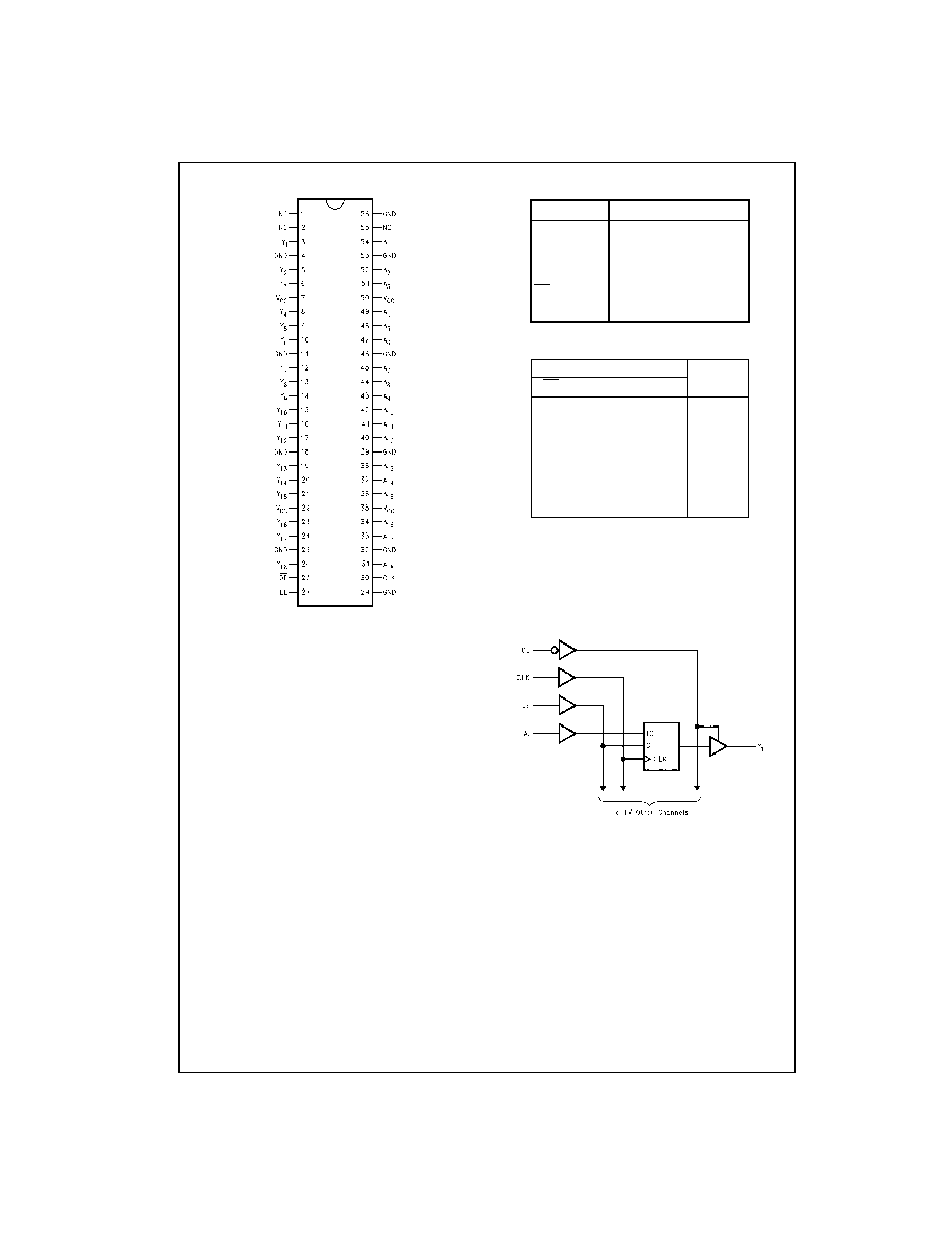
Connection Diagram
Pin Descriptions
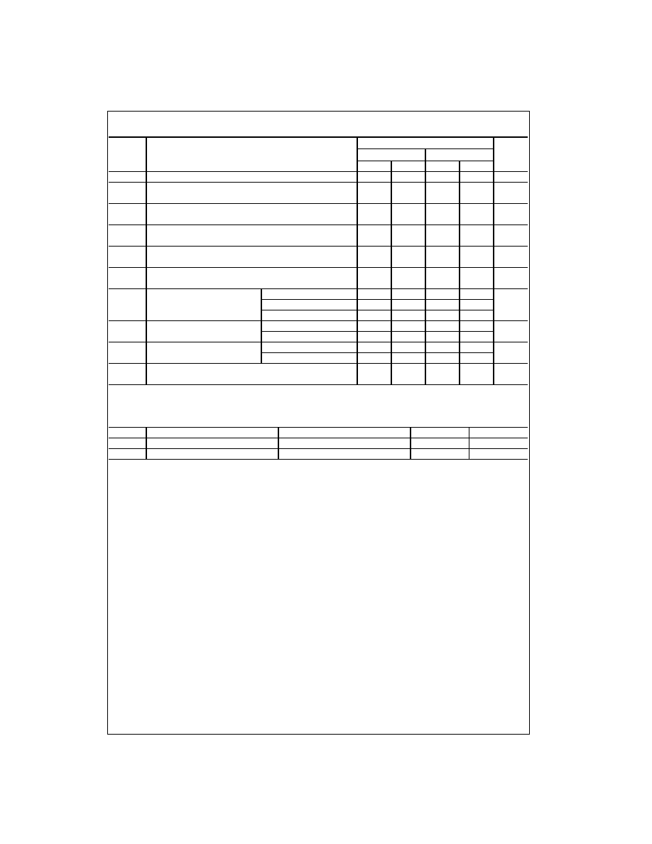
Truth Table
H
=
HIGH Voltage Level
L
=
LOW Voltage Level
X
=
Immaterial
Z
=
High Impedance
=
HIGH-to-LOW Clock Transition
Note 1: Output level before the indicated steady-state input conditions
were established, provided that CLK was HIGH before LE went LOW.
Note 2: Output level before the indicated steady-state input conditions
were established.
Logic Diagram
Pin Names
Description
A
1
A
18
Data Register Inputs
Y
1
Y
18
3-STATE Outputs
CLK
Clock Pulse Input
OE
Output Enable Input
LE
Latch Enable Input
Inputs
Output
Y
OE
LE
CLK
A
H
X
X
X
Z
L
H
X
L
L
L
H
X
H
H
L
L
L
L
L
L
H
H
L
L
H
X
Y
0
(Note 1)
L
L
L
X
Y
0
(Note 2)
Preliminary
3
www.fairchildsemi.com
7
4
L
V
TH16
835
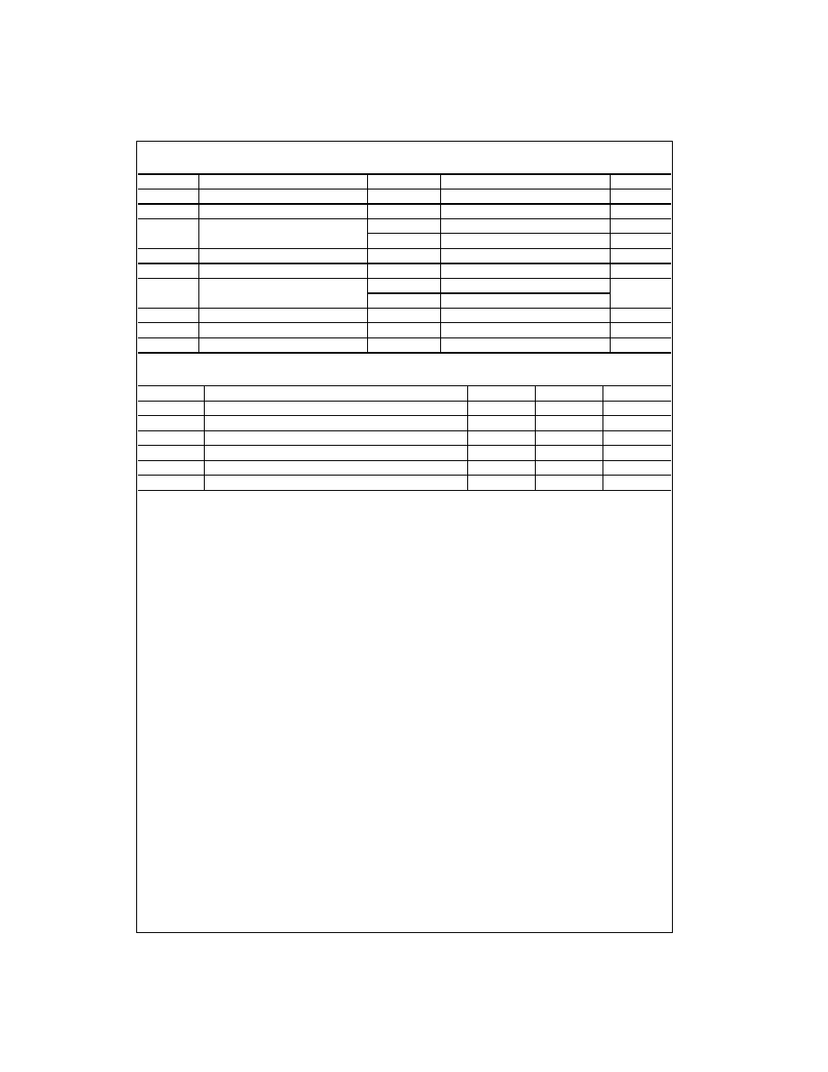
Absolute Maximum Ratings
(Note 3)
Recommended Operating Conditions
Note 3: Absolute Maximum continuous ratings are those values beyond which damage to the device may occur. Exposure to these conditions or conditions
beyond those indicated may adversely affect device reliability. Functional operation under absolute maximum rated conditions is not implied.
Note 4: I
O
Absolute Maximum Rating must be observed.
Symbol
Parameter
Value
Conditions
Units
V
CC
Supply Voltage
-
0.5 to
+
4.6
V
V
I
DC Input Voltage
-
0.5 to
+
7.0
V
V
O
DC Output Voltage
-
0.5 to
+
7.0
Output in 3-STATE
V
-
0.5 to
+
7.0
Output in HIGH or LOW State (Note 4)
V
I
IK
DC Input Diode Current
-
50
V
I
<
GND
mA
I
OK
DC Output Diode Current
-
50
V
O
<
GND
mA
I
O
DC Output Current
64
V
O
>
V
CC
Output at HIGH State
mA
128
V
O
>
V
CC
Output at LOW State
I
CC
DC Supply Current per Supply Pin
±
64
mA
I
GND
DC Ground Current per Ground Pin
±
128
mA
T
STG
Storage Temperature
-
65 to
+
150
°
C
Symbol
Parameter
Min
Max
Units
V
CC
Supply Voltage
2.7
3.6
V
V
I
Input Voltage
0
5.5
V
I
OH
HIGH-Level Output Current
-
32
mA
I
OL
LOW-Level Output Current
64
mA
T
A
Free-Air Operating Temperature
-
40
85
°
C
t/
V
Input Edge Rate, V
IN
=
0.8V2.0V, V
CC
=
3.0V
0
10
ns/V
Preliminary
www.fairchildsemi.com
4
74L
VTH16835
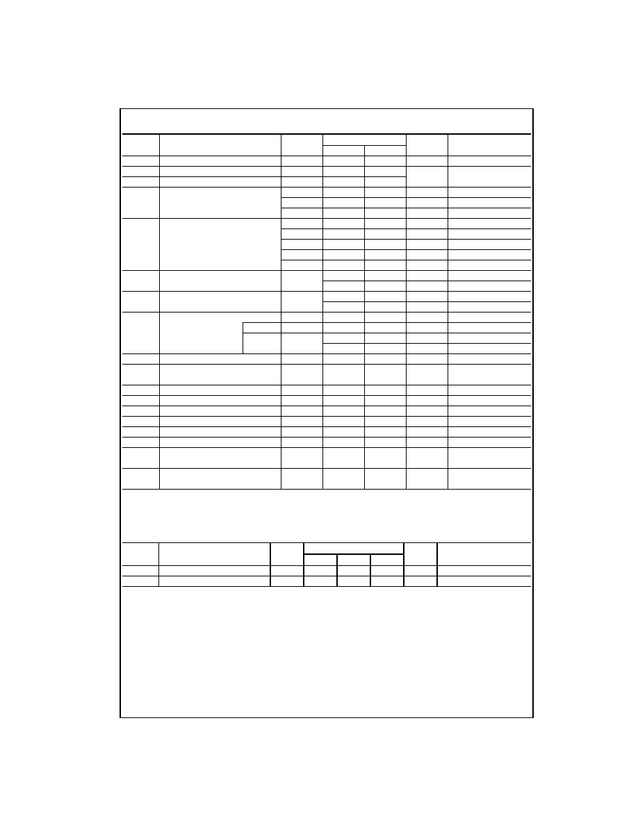
DC Electrical Characteristics
Note 5: An external driver must source at least the specified current to switch from LOW-to-HIGH.
Note 6: An external driver must sink at least the specified current to switch from HIGH-to-LOW.
Note 7: This is the increase in supply current for each input that is at the specified voltage level rather than V
CC
or GND.
Dynamic Switching Characteristics
(Note 8)
Note 8: Characterized in SSOP package. Guaranteed parameter, but not tested.
Note 9: Max number of outputs defined as (n). n
-
1 data inputs are driven 0V to 3V. Output under test held LOW.
Symbol
Parameter
V
CC
T
A
=
-
40
°
C to
+
85
°
C
Units
Conditions
(V)
Min
Max
V
IK
Input Clamp Diode Voltage
2.7
-
1.2
V
I
I
=
-
18 mA
V
IH
Input HIGH Voltage
2.73.6
2.0
V
V
O
0.1V or
V
IL
Input LOW Voltage
2.73.6
0.8
V
O
V
CC
-
0.1V
V
OH
Output HIGH Voltage
2.73.6
V
CC
-
0.2
V
I
OH
=
-
100
µ
A
2.7
2.4
V
I
OH
=
-
8 mA
3.0
2.0
V
I
OH
=
-
32 mA
V
OL
Output LOW Voltage
2.7
0.2
V
I
OL
=
100
µ
A
2.7
0.5
V
I
OL
=
24 mA
3.0
0.4
V
I
OL
=
16 mA
3.0
0.5
V
I
OL
=
32 mA
3.0
0.55
V
I
OL
=
64 mA
I
I(HOLD)
Bushold Input Minimum Drive
3.0
75
µ
A
V
I
=
0.8V
-
75
µ
A
V
I
=
2.0V
I
I(OD)
Bushold Input Over-Drive
Current to Change State
3.0
500
µ
A
(Note 5)
-
500
µ
A
(Note 6)
I
I
Input Current
3.6
10
µ
A
V
I
=
5.5V
Control Pins
3.6
±
1
µ
A
V
I
=
0V or V
CC
Data Pins
3.6
-
5
µ
A
V
I
=
0V
1
µ
A
V
I
=
V
CC
I
OFF
Power Off Leakage Current
0
±
100
µ
A
0V
V
I
or V
O
5.5V
I
PU/PD
Power up/down 3-STATE
01.5V
±
100
µ
A
V
O
=
0.5V to 3.0V
Output Current
V
I
=
GND or V
CC
I
OZL
3-STATE Output Leakage Current
3.6
-
5
µ
A
V
O
=
0.5V
I
OZH
3-STATE Output Leakage Current
3.6
5
µ
A
V
O
=
3.0V
I
OZH
+
3-STATE Output Leakage Current
3.6
10
µ
A
V
CC
<
V
O
5.5V
I
CCH
Power Supply Current
3.6
0.19
mA
Outputs HIGH
I
CCL
Power Supply Current
3.6
5
mA
Outputs LOW
I
CCZ
Power Supply Current
3.6
0.19
mA
Outputs Disabled
I
CCZ
+
Power Supply Current
3.6
0.19
mA
V
CC
V
O
5.5V,
Outputs Disabled
I
CC
Increase in Power Supply Current
3.6
0.2
mA
One Input at V
CC
-
0.6V
(Note 7)
Other Inputs at V
CC
or GND
Symbol
Parameter
V
CC
T
A
=
25
°
C
Units
Conditions
(V)
Min
Typ
Max
C
L
=
50 pF, R
L
=
500
V
OLP
Quiet Output Maximum Dynamic V
OL
3.3
0.8
V
(Note 9)
V
OLV
Quiet Output Minimum Dynamic V
OL
3.3
-
0.8
V
(Note 9)
Preliminary
5
www.fairchildsemi.com
7
4
L
V
TH16
835
AC Electrical Characteristics
Note 10: Skew is defined as the absolute value of the difference between the actual propagation delay for any two separate outputs of the same device. The
specification applies to any outputs switching in the same direction, either HIGH-to-LOW (t
OSHL
) or LOW-to-HIGH (t
OSLH
).
Capacitance
(Note 11)
Note 11: Capacitance is measured at frequency f
=
1 MHz, per MIL-STD-883, Method 3012.
Symbol
Parameter
T
A
=
-
40
°
C to
+
85
°
C, C
L
=
50 pF, R
L
=
500
Units
V
CC
=
3.3
±
0.3V
V
CC
=
2.7V
Min
Max
Min
Max
f
MAX
150
150
MHz
t
PLH
Propagation Delay
1.3
3.7
1.3
4.0
ns
t
PHL
A to Y
1.3
3.7
1.3
4.0
t
PLH
Propagation Delay
1.5
5.1
1.5
5.7
ns
t
PHL
LE to Y
1.5
5.1
1.5
5.7
t
PLH
Propagation Delay
1.5
5.1
1.5
5.7
ns
t
PHL
CLK to Y
1.5
5.1
1.5
5.7
t
PZH
Output Enable Time
1.3
4.6
1.3
5.5
ns
t
PZL
1.3
4.6
1.3
5.5
t
PHZ
Output Disable Time
1.7
5.8
1.7
6.3
ns
t
PLZ
1.7
5.8
1.7
6.3
t
S
Setup Time
A before CLK
2.1
2.4
ns
A before LE, CLK HIGH
2.3
1.5
A before LE, CLK LOW
1.5
0.5
t
H
Hold Time
A after CLK
1.0
0.0
ns
A after LE
0.8
0.8
t
W
Pulse Duration
LE HIGH
3.3
3.3
ns
CLK HIGH or LOW
3.3
3.3
t
OSLH
Output to Output Skew
1.0
1.0
ns
t
OSHL
(Note 10)
1.0
1.0
Symbol
Parameter
Conditions
Typical
Units
C
IN
Input Capacitance
V
CC
=
0V, V
I
=
0V or V
CC
4
pF
C
OUT
Output Capacitance
V
CC
=
3.0V, V
O
=
0V or V
CC
8
pF