 | –≠–ª–µ–∫—Ç—Ä–æ–Ω–Ω—ã–π –∫–æ–º–ø–æ–Ω–µ–Ω—Ç: 74LVX157 | –°–∫–∞—á–∞—Ç—å:  PDF PDF  ZIP ZIP |

© 2003 Fairchild Semiconductor Corporation
DS011608
www.fairchildsemi.com
May 1993
Revised October 2003
7
4
L
VX15
7
Low
V
o
l
t
a
g
e Quad
2-I
nput
Mult
i
p
lexer
74LVX157
Low Voltage Quad 2-Input Multiplexer
General Description
The LVX157 is a high-speed quad 2-input multiplexer. Four
bits of data from two sources can be selected using the
common Select and Enable inputs. The four outputs
present the selected data in the true (noninverted) form.
The LVX157 can also be used as a function generator.
Features
s
Input voltage level translation from 5V to 3V
s
Ideal for low power/low noise 3.3V applications
s
Guaranteed simultaneous switching noise level and
dynamic threshold performance
Ordering Code:
Devices are also available in Tape and Reel. Specify by appending letter suffix "X" to the ordering code.
Logic Symbols
IEEE/IEC
Connection Diagram
Pin Descriptions
Order Number
Package Number
Package Description
74LVX157M
M16A
16-Lead Small Outline Integrated Circuit (SOIC), JEDEC MS-012, 0.150" Narrow
74LVX157SJ
M16D
16-Lead Small Outline Package (SOP), EIAJ TYPE II, 5.3mm Wide
74LVX157MTC
MTC16
16-Lead Thin Shrink Small Outline Package (TSSOP), JEDEC MO-153, 4.4mm Wide
Pin Names
Description
I
0a
≠I
0d
Source 0 Data Inputs
I
1a
≠I
1d
Source 1 Data Inputs
E
Enable Input
S
Select Input
Z
a
≠Z
d
Outputs

www.fairchildsemi.com
2
74
L
VX157
Truth Table
H
=
HIGH Voltage Level
L
=
LOW Voltage Level
X
=
Immaterial
Functional Description
The LVX157 is a quad 2-input multiplexer. It selects four
bits of data from two sources under the control of a com-
mon Select input (S). The Enable input (E) is active-LOW.
When E is HIGH, all of the outputs (Z) are forced LOW
regardless of all other inputs. The LVX157 is the logic
implementation of a 4-pole, 2-position switch where the
position of the switch is determined by the logic levels sup-
plied to the Select input. The logic equations for the outputs
are shown below:
Z
a
=
E ∑ (I
1a
∑ S
+
I
0a
∑ S)
Z
b
=
E ∑ (I
1b
∑ S
+
I
0b
∑ S)
Z
c
=
E ∑ (I
1c
∑ S
+
I
0c
∑ S)
Z
d
=
E ∑ (I
1d
∑ S
+
I
0d
∑ S)
A common use of the LVX157 is the moving of data from
two groups of registers to four common output busses. The
particular register from which the data comes is determined
by the state of the Select input. A less obvious use is as a
function generator. The LVX157 can generate any four of
the sixteen different functions of two variables with one
variable common. This is useful for implementing gating
functions.
Logic Diagram
Inputs
Outputs
E
S
I
0
I
1
Z
H
X
X
X
L
L
H
X
L
L
L
H
X
H
H
L
L
L
X
L
L
L
H
X
H

3
www.fairchildsemi.com
74
L
V
X
1
57
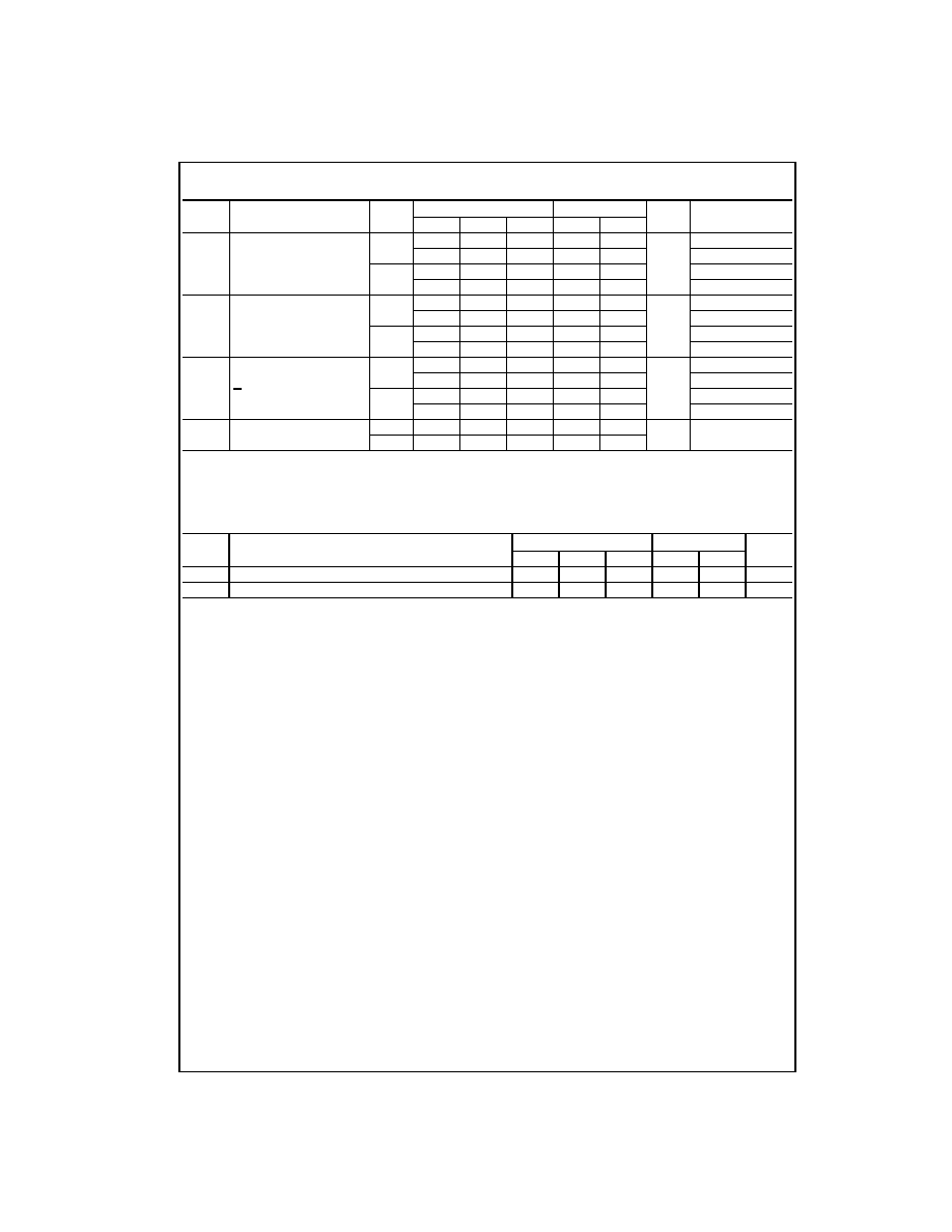
Absolute Maximum Ratings
(Note 1)
Recommended Operating
Conditions
(Note 2)
Note 1: The "Absolute Maximum Ratings" are those values beyond which
the safety of the device cannot be guaranteed. The device should not be
operated at these limits. The parametric values defined in the Electrical
Characteristics tables are not guaranteed at the absolute maximum ratings.
The "Recommended Operating Conditions" table will define the conditions
for actual device operation.
Note 2: Unused inputs must be held HIGH or LOW. They may not float.
DC Electrical Characteristics
Noise Characteristics
(Note 3)
Note 3: Input t
r
=
t
f
=
3ns
Supply Voltage (V
CC
)
-
0.5V to
+
7.0V
DC Input Diode Current (I
IK
)
V
I
=
-
0.5V
-
20 mA
DC Input Voltage (V
I
)
-
0.5V to 7V
DC Output Diode Current (I
OK
)
V
O
=
-
0.5V
-
20 mA
V
O
=
V
CC
+
0.5V
+
20 mA
DC Output Voltage (V
O
)
-
0.5V to V
CC
+
0.5V
DC Output Source
or Sink Current (I
O
)
±
25 mA
DC V
CC
or Ground Current
(I
CC
or I
GND
)
±
50 mA
Storage Temperature (T
STG
)
-
65
∞
C to
+
150
∞
C
Power Dissipation
180 mW
Supply Voltage (V
CC
)
2.0V to 3.6V
Input Voltage (V
I
)
0V to 5.5V
Output Voltage (V
O
)
0V to V
CC
Operating Temperature (T
A
)
-
40
∞
C to
+
85
∞
C
Input Rise and Fall Time (
t/
V)
0 ns/V to 100 ns/V
Symbol
Parameter
V
CC
T
A
=
+
25
∞
C T
A
=
-
40
∞
C to
+
85
∞
C
Units
Conditions
Min
Typ
Max
Min
Max
V
IH
HIGH Level
2.0
1.5
1.5
Input Voltage
3.0
2.0
2.0
V
3.6
2.4
2.4
V
IL
LOW Level
2.0
0.5
0.5
Input Voltage
3.0
0.8
0.8
V
3.6
0.8
0.8
V
OH
HIGH Level
2.0
1.9
2.0
1.9
V
IN
=
V
IL
or V
IH
I
OH
=
-
50
µ
A
Output Voltage
3.0
2.9
3.0
2.9
V
I
OH
=
-
50
µ
A
3.0
2.58
2.48
I
OH
=
-
4 mA
V
OL
LOW Level
2.0
0.0
0.1
0.1
V
IN
=
V
IL
or V
IH
I
OL
=
50
µ
A
Output Voltage
3.0
0.0
0.1
0.1
V
I
OL
=
50
µ
A
3.0
0.36
0.44
I
OL
=
4 mA
I
IN
Input Leakage Current
3.6
±
0.1
±
1.0
µ
A
V
IN
=
5.5V or GND
I
CC
Quiescent Supply Current
3.6
4.0
40.0
µ
A
V
IN
=
V
CC
or GND
Symbol
Parameter
V
CC
T
A
=
25
∞
C
Units
C
L
(pF)
(V)
Typ
Limit
V
OLP
Quiet Output Maximum Dynamic V
OL
3.3
0.3
0.5
V
50
V
OLV
Quiet Output Minimum Dynamic V
OL
3.3
-
0.3
-
0.5
V
50
V
IHD
Minimum HIGH Level Dynamic Input Voltage
3.3
2.0
V
50
V
ILD
Maximum LOW Level Dynamic Input Voltage
3.3
0.8
V
50
www.fairchildsemi.com
4
74
L
VX157
AC Electrical Characteristics
Note 4: Parameter guaranteed by design.
t
OSLH
=
|t
PLHm
-
t
PLHn
|.
t
OSHL
=
|t
PHLm
-
t
PHLn
|.
Capacitance
Note 5: C
PD
is defined as the value of the internal equivalent capacitance which is calculated from the operating current consumption without load.
Average operating current can be obtained by the equation: I
CC(opr.)
=
C
PD
◊
V
CC
◊
f
IN
+
I
CC
Symbol
Parameter
V
CC
T
A
=
+
25
∞
C T
A
=
-
40
∞
C to
+
85
∞
C
Units
C
L
(pF)
(V)
Min
Typ
Max
Min
Max
t
PLH
Propagation
2.7
6.6
12.5
1.0
15.5
ns
15
t
PHL
Delay Time
9.1
16.0
1.0
19.0
50
I
n
to Z
n
3.3
±
0.3
5.1
7.9
1.0
9.5
15
7.6
11.4
1.0
13.0
50
t
PLH
Propagation
2.7
8.9
16.9
1.0
20.5
ns
15
t
PHL
Delay Time
11.4
20.4
1.0
24.0
50
S to Z
n
3.3
±
0.3
7.0
11.0
1.0
13.0
15
9.5
14.5
1.0
16.5
50
t
PLH
t
PHL
Propagation
2.7
9.1
17.6
1.0
20.5
ns
15
Delay Time
11.6
21.1
1.0
24.0
50
E to Z
n
3.3
±
0.3
7.2
11.5
1.0
13.5
15
9.7
15.0
1.0
17.0
50
t
OSHL
Output to Output
2.7
1.5
1.5
ns
50
t
OSLH
Skew (Note 4)
3.3
1.5
1.5
Symbol
Parameter
T
A
=
+
25
∞
C T
A
=
-
40
∞
C to
+
85
∞
C
Units
Min
Typ
Max
Min
Max
C
IN
Input Capacitance
4
10
10
pF
C
PD
Power Dissipation Capacitance (Note 5)
20
pF

5
www.fairchildsemi.com
74
L
V
X
1
57
Physical Dimensions
inches (millimeters) unless otherwise noted
16-Lead Small Outline Integrated Circuit (SOIC), JEDEC MS-012, 0.150" Narrow
Package Number M16A