
November 1992
Revised April 1999
7
4
VH
C15
7
Quad
2-I
nput
Mult
ip
lexer
© 1999 Fairchild Semiconductor Corporation
DS011536.prf
www.fairchildsemi.com
74VHC157
Quad 2-Input Multiplexer
General Description
The VHC157 is an advanced high speed CMOS Quad 2-
Channel Multiplexer fabricated with silicon gate CMOS
technology. It achieves the high speed operation similar to
equivalent Bipolar Schottky TTL while maintaining the
CMOS low power dissipation.
It consists of four 2-input digital multiplexers with common
select and enable inputs. When the ENABLE input is held
"H" level, selection of data is inhibited and all the outputs
become "L" level. The SELECT decoding determines
whether the I
0x
or I
1x
inputs get routed to their correspond-
ing outputs.
An Input protection circuit ensures that 0V to 7V can be
applied to the input pins without regard to the supply volt-
age. This device can be used to interface 5V to 3V systems
and on two supply systems such as battery back up. This
circuit prevents device destruction due to mismatched sup-
ply and input voltages.
Features
s
High Speed: t
PD
=
4.1 ns (typ) at V
CC
=
5V
s
Low power dissipation: I
CC
=
4
µ
A (max.) at T
A
=
25
∞
C
s
High noise immunity: V
NIH
=
V
NIL
=
28% V
CC
(min.)
s
Power down protection is provided on all inputs
s
Low noise: V
OLP
=
0.8V (max.)
s
Pin and function compatible with 74HC157
Ordering Code:
Surface mount packages are also available on Tape and Reel. Specify by appending the suffix letter "X" to the ordering code.
Logic Symbols
IEEE/IEC
Connection Diagram
Pin Descriptions
Order Number
Package Number
Package Description
74VHC157M
M16A
16-Lead Small Outline Integrated Circuit (SOIC), JEDEC MS-012, 0.150" Narrow
74VHC157SJ
M16D
16-Lead Small Outline Package (SOP), EIAJ TYPE II, 5.3mm Wide
74VHC157MTC
MTC16
16-Lead Thin Shrink Small Outline Package (TSSOP), JEDEC MO-153, 4.4mm Wide
74VHC157N
N16E
16-Lead Plastic Dual-In-Line Package (PDIP), JEDEC MS-001, 0.300" Wide
Pin Names
Description
I
0a
≠I
0d
Source 0 Data Inputs
I
1a
≠I
1d
Source 1 Data Inputs
E
Enable Input
S
Select Input
Z
a
≠Z
d
Outputs

www.fairchildsemi.com
2
74
V
HC157
Truth Table
H
=
HIGH Voltage Level
L
=
LOW Voltage Level
X
=
Immaterial
Functional Description
The VHC157 is a quad 2-input multiplexer. It selects four
bits of data from two sources under the control of a com-
mon Select input (S). The Enable input (E) is active-LOW.
When E is HIGH, all of the outputs (Z) are forced LOW
regardless of all other inputs. The VHC157 is the logic
implementation of a 4-pole, 2-position switch where the
position of the switch is determined by the logic levels sup-
plied to the Select input. The logic equations for the outputs
are shown below:
Z
a
=
E ∑ (I
1a
∑ S
+
I
0a
∑ S)
Z
b
=
E ∑ (I
1b
∑ S
+
I
0b
∑ S)
Z
c
=
E ∑ (I
1c
∑ S
+
I
0c
∑ S)
Z
d
=
E ∑ (I
1d
∑ S
+
I
0d
∑ S)
A common use of the VHC157 is the moving of data from
two groups of registers to four common output busses. The
particular register from which the data comes is determined
by the state of the Select input. A less obvious use is as a
function generator. The VHC157 can generate any four of
the sixteen different functions of two variables with one
variable common. This is useful for implementing gating
functions.
Logic Diagram
Please note that this diagram is provided only for the understanding of logic operations and should not be used to estimate propagation delays.
Inputs
Outputs
E
S
I
0
I
1
Z
H
X
X
X
L
L
H
X
L
L
L
H
X
H
H
L
L
L
X
L
L
L
H
X
H
3
www.fairchildsemi.com
7
4
VH
C15
7
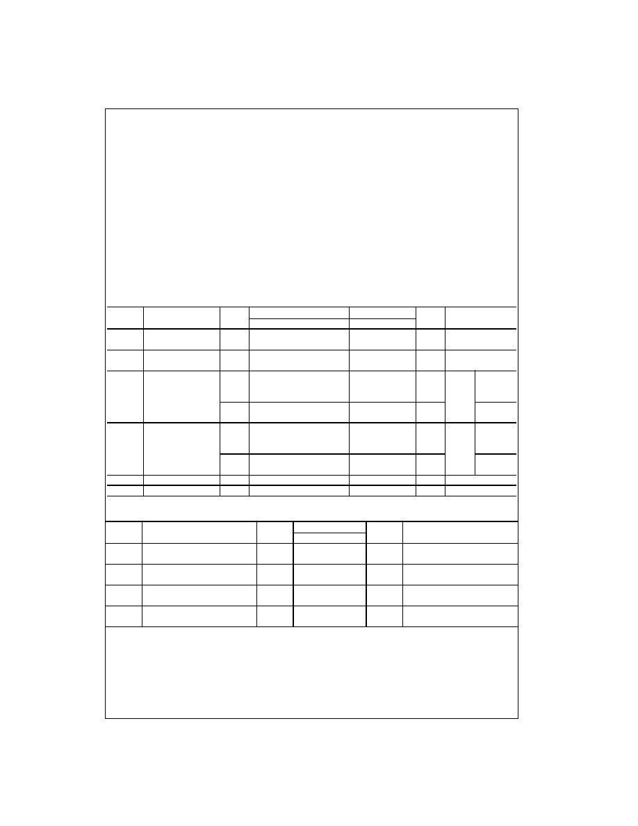
Absolute Maximum Ratings
(Note 1)
Recommended Operating
Conditions
(Note 2)
Note 1: Absolute Maximum Ratings are values beyond which the device
may be damaged or have its useful life impaired. The databook specifica-
tions should be met, without exception, to ensure that the system design is
reliable over its power supply, temperature, and output/input loading vari-
ables. Fairchild does not recommend operation outside databook specifica-
tions.
Note 2: Unused inputs must be held HIGH or LOW. They may not float.
DC Electrical Characteristics
Noise Characteristics
Note 3: Parameter guaranteed by design.
Supply Voltage (V
CC
)
-
0.5V to
+
7.0V
DC Input Voltage (V
IN
)
-
0.5V to
+
7.0V
DC Output Voltage (V
OUT
)
-
0.5V to V
CC
+
0.5V
Input Diode Current (I
IK
)
-
20 mA
Output Diode Current (I
OK
)
±
20 mA
DC Output Current (I
OUT
)
±
25 mA
DC V
CC
/GND Current (I
CC
)
±
50 mA
Storage Temperature (T
STG
)
-
65
∞
C to
+
150
∞
C
Lead Temperature (T
L
)
(Soldering, 10 seconds)
260
∞
C
Supply Voltage (V
CC
)
2.0V to
+
5.5V
Input Voltage (V
IN
)
0V to
+
5.5V
Output Voltage (V
OUT
)
0V to V
CC
Operating Temperature (T
OPR
)
-
40
∞
C to
+
85
∞
C
Input Rise and Fall Time (t
r
, t
f
)
V
CC
=
3.3V
±
0.3V
0
100 ns/V
V
CC
=
5.0V
±
0.5V
0
20 ns/V
Symbol
Parameter
V
CC
(V)
T
A
=
25
∞
C
T
A
=
-
40
∞
C to
+
85
∞
C
Units
Conditions
Min
Typ
Max
Min
Max
V
IH
HIGH Level
2.0
1.50
1.50
V
Input Voltage
3.0
-
5.5
0.7 V
CC
0.7 V
CC
V
IL
LOW Level
2.0
0.50
0.50
V
Input Voltage
3.0
-
5.5
0.3 V
CC
0.3 V
CC
V
OH
HIGH Level
2.0
1.9
2.0
1.9
V
IN
=
V
IH
I
OH
=
-
50
µ
A
Output Voltage
3.0
2.9
3.0
2.9
V
or V
IL
4.5
4.4
4.5
4.4
3.0
2.58
2.48
V
I
OH
=
-
4 mA
4.5
3.94
3.80
I
OH
=
-
8 mA
V
OL
LOW Level
2.0
0.0
0.1
0.1
V
IN
=
V
IH
I
OL
=
50
µ
A
Output Voltage
3.0
0.0
0.1
0.1
V
or V
IL
4.5
0.0
0.1
0.1
3.0
0.36
0.44
V
I
OL
=
4 mA
4.5
0.36
0.44
I
OL
=
8 mA
I
IN
Input Leakage Current
0
-
5.5
±
0.1
±
1.0
µ
A
V
IN
=
5.5V or GND
I
CC
Quiescent Supply Current
5.5
4.0
40.0
µ
A
V
IN
=
V
CC
or GND
Symbol
Parameter
V
CC
(V)
T
A
=
25
∞
C
Units
Conditions
Typ
Limits
V
OLP
Quiet Output Maximum
5.0
0.3
0.8
V
C
L
=
50 pF
(Note 3)
Dynamic V
OL
V
OLV
Quiet Output Minimum
5.0
-
0.3
-
0.8
V
C
L
=
50 pF
(Note 3)
Dynamic V
OL
V
IHD
Minimum HIGH Level
5.0
3.5
V
C
L
=
50 pF
(Note 3)
Dynamic Input Voltage
V
ILD
Maximum LOW Level
5.0
1.5
V
C
L
=
50 pF
(Note 3)
Dynamic Input Voltage

www.fairchildsemi.com
4
74
V
HC157
AC Electrical Characteristics
Note 4: C
PD
is defined as the value of the internal equivalent capacitance which is calculated from the operating current consumption without load. Average
operating current can be obtained by the equation: I
CC
(opr.)
=
C
PD
* V
CC
* f
IN
+
I
CC
.
Symbol
Parameter
V
CC
(V)
T
A
=
25
∞
C
T
A
=
-
40
∞
C to
+
85
∞
C
Units
Conditions
Min
Typ
Max
Min
Max
t
PLH
Propagation Delay
3.3
±
0.3
6.2
9.7
1.0
11.5
ns
C
L
=
15 pF
t
PHL
I
n
to Z
n
8.7
13.2
1.0
15.0
C
L
=
50 pF
5.0
±
0.5
4.1
6.4
1.0
7.5
ns
C
L
=
15 pF
5.6
8.4
1.0
9.5
C
L
=
50 pF
t
PLH
Propagation Delay
3.3
±
0.3
8.4
13.2
1.0
15.5
ns
C
L
=
15 pF
t
PHL
S to Z
n
10.9
16.7
1.0
19.0
C
L
=
50 pF
5.0
±
0.5
5.3
8.1
1.0
9.5
ns
C
L
=
15 pF
6.8
10.1
1.0
11.5
C
L
=
50 pF
t
PLH
Propagation Delay
3.3
±
0.3
8.7
13.6
1.0
16.0
ns
C
L
=
15 pF
t
PHL
E to Z
n
11.2
17.1
1.0
19.5
C
L
=
50 pF
5.0
±
0.5
5.6
8.6
1.0
10.0
ns
C
L
=
15 pF
7.1
10.6
1.0
12.0
C
L
=
50 pF
C
IN
Input Capacitance
4
10
10
pF
V
CC
=
Open
C
PD
Power Dissipation
20
pF
(Note 4)
Capacitance

5
www.fairchildsemi.com
7
4
VH
C15
7
Physical Dimensions
inches (millimeters) unless otherwise noted
16-Lead Small Outline Integrated Circuit (SOIC), JEDEC MS-012, 0.150" Narrow
Package Number M16A
16-Lead Small Outline Package (SOP), EIAJ TYPE II, 5.3mm Wide
Package Number M16D