© 2005 Fairchild Semiconductor Corporation
DS500098
www.fairchildsemi.com
February 1998
Revised June 2005
7
4
VH
C16
1284 I
EEE 12
84 T
r
anscei
ver
74VHC161284
IEEE 1284 Transceiver
General Description
The VHC161284 contains eight bidirectional data buffers
and eleven control/status buffers to implement a full
IEEE 1284 compliant interface. The device supports the
IEEE 1284 standard and is intended to be used in
Extended Capabilities Port mode (ECP). The pinout allows
for easy connection from the Peripheral (A-side) to the
Host (cable side).
Outputs on the cable side can be configured to be either
open drain or high drive (
r
14 mA). The pull-up and pull-
down series termination resistance of these outputs on the
cable side is optimized to drive an external cable. In addi-
tion, all inputs (except HLH) and outputs on the cable side
contain internal pull-up resistors connected to the V
CC
sup-
ply to provide proper termination and pull-ups for open
drain mode.
Outputs on the Peripheral side are standard LOW-drive
CMOS outputs. The DIR input controls data flow on the A
1
≠
A
8
/B
1
≠B
8
transceiver pins.
Features
s
Supports IEEE 1284 Level 1 and Level 2 signaling
standards for bidirectional parallel communications
between personal computers and printing peripherals
s
Replaces the function of two (2) 74ACT1284 devices
s
All inputs have hysteresis to provide noise margin
s
B and Y output resistance optimized to drive external
cable
s
B and Y outputs in high impedance mode during power
down
s
Inputs and outputs on cable side have internal pull-up
resistors
s
Flow-through pin configuration allows easy interface
between the Peripheral and Host
Ordering Code:
Surface mount packages are also available on Tape and Reel. Specify by appending the suffix letter "X" to the ordering code.
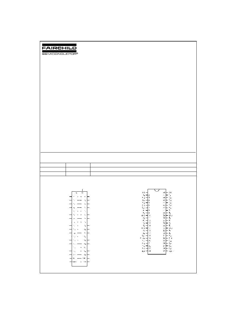
Logic Symbol
Connection Diagram
Ordering Number Package Number
Package Description
74VHC161284MEA
MS48A
48-Lead Small Shrink Outline Package (SSOP), JEDEC MO-118, 0.300" Wide
74VHC161284MTD
MTD48
48-Lead Thin Shrink Small Outline Package (TSSOP), JEDEC MO-153, 6.1mm Wide
www.fairchildsemi.com
2
74VHC161284
Pin Descriptions
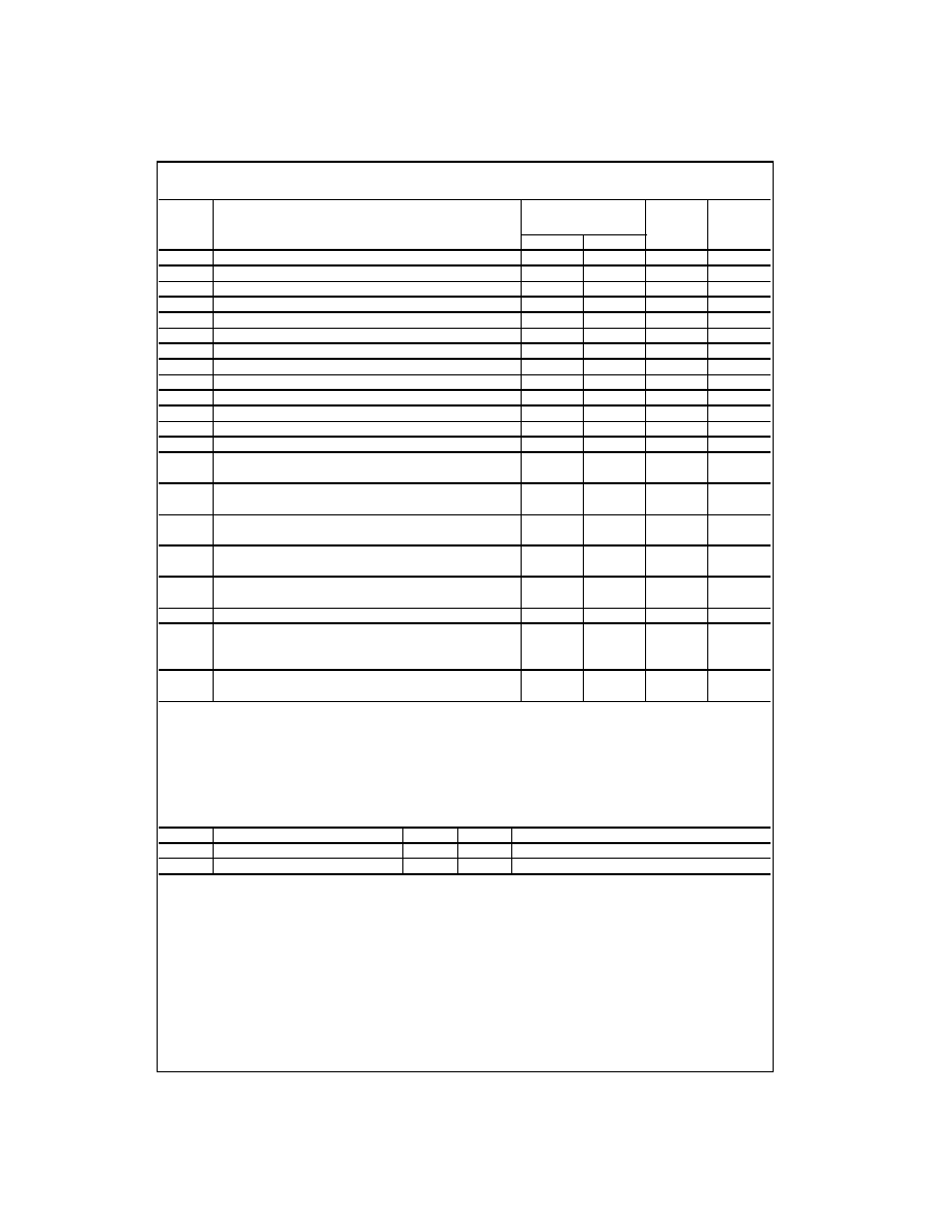
Truth Table
Note 1: Y
9
≠Y
13
Open Drain Outputs
Note 2: B
1
≠B
8
Open Drain Outputs
Logic Diagram
Pin Names
Description
HD
HIGH Drive Enable Input (Active HIGH)
DIR
Direction Control Input
A
1
≠A
8
Inputs or Outputs
B
1
≠B
8
Inputs or Outputs
A
9
≠A
13
Inputs
Y
9
≠Y
13
Outputs
A
14
≠A
17
Outputs
C
14
≠C
17
Inputs
PLH
IN
Peripheral Logic HIGH Input
PLH
Peripheral Logic HIGH Output
HLH
IN
Host Logic HIGH Input
HLH
Host Logic HIGH Output
Inputs
Outputs
DIR
HD
L
L
B
1
≠B
8
Data to A
1
≠A
8
, and
A
9
≠A
13
Data to Y
9
≠Y
13
(Note 1)
C
14
≠C
17
Data to A
14
≠A
17
PLH Open Drain Mode
L
H
B
1
≠B
8
Data to A
1
≠A
8
, and
A
9
≠A
13
Data to Y
9
≠Y
13
C
14
≠C
17
Data to A
14
≠A
17
H
L
A
1
≠A
8
Data to B
1
≠B
8
(Note 2)
A
9
≠A
13
Data to Y
9
≠Y
13
(Note 1)
C
14
≠C
17
Data to A
14
≠A
17
PLH Open Drain Mode
H
H
A
1
≠A
8
Data to B
1
≠B
8
A
9
≠A
13
Data to Y
9
≠Y
13
C
14
≠C
17
Data to A
14
≠A
17
3
www.fairchildsemi.com
7
4
VH
C16
1284
Absolute Maximum Ratings
(Note 3)
Recommended Operating
Conditions
Note 3: Absolute Maximum continuos ratings are those values beyond
which damage to the device may occur. Exposure to these indicated may
adversely affect device reliability. Functional operation under absolute max-
imum rated conditions is not implied.
Note 4: Either voltage limit or current limit is sufficient to protect inputs.
DC Electrical Characteristics
Supply Voltage
V
CC
0.5V to
7.0V
Input Voltage (V
I
) (Note 4)
A
1
≠A
13
, PLH
IN
, DIR, HD
0.5V to V
CC
0.5V
B
1
≠B
8
, C
14
≠C
17
, HLH
IN
0.5V to
5.5V (DC)
B
1
≠B
8
, C
14
≠C
17
, HLH
IN
2.0V to
7.0V *
*40 ns Transient
Output Voltage (V
O
)
A
1
≠A
8
, A
14
≠A
17
, HLH
0.5V to V
CC
0.5V
B
1
≠B
8
, Y
9
≠Y
13
, PLH
0.5V to
5.5V (DC)
B
1
≠B
8
, Y
9
≠Y
13
, PLH
2.0V to
7.0V*
*40 ns Transient
DC Output Current (I
O
)
A
1
≠A
8
, HLH
r
25 mA
B
1
≠B
8
, Y
9
≠Y
13
r
50 mA
PLH (Output LOW)
84 mA
PLH (Output HIGH)
50 mA
Input Diode Current (I
IK
) (Note 4)
DIR, HD, A
9
≠A
13
,
PLH, HLH, C
14
≠C
17
20 mA
Output Diode Current (I
OK
)
A
1
≠A
8
, A
14
≠A
17
, HLH
r
50 mA
B
1
≠B
8
, Y
9
≠Y
13
, PLH
50 mA
DC Continuous V
CC
or
Ground Current
r
200 mA
Storage Temperature
65
q
C to
150
q
C
ESD (HBM) Last Passing
Voltage
2000V
Supply Voltage
V
CC
4.5V to 5.5V
DC Input Voltage (V
I
) 0V
to
V
CC
Open Drain Voltage (V
O
) 0V
to
5.5V
Operating Temperature (T
A
)
40
q
C to
85
q
C
Symbol Parameter
V
CC
T
A
40
q
C to
85
q
C
Units
Conditions
(V)
Guaranteed Limits
V
IK
Input Clamp Diode Voltage
3.0
1.2
V
I
I
18 mA
V
IH
Minimum HIGH Level Input Voltage
A
n
, PLH
IN
, DIR, HD
4.5
5.5
0.7 V
CC
V
B
n
4.5
5.5
2.0
C
n
4.5
5.5
2.3
HLH
IN
4.5
5.5
2.6
V
IL
Maximum LOW Level Input Voltage
A
n
, PLH
IN
, DIR, HD
4.5
5.5
0.3 V
CC
V
B
n
4.5
5.5
0.8
C
n
4.5
5.5
0.8
HLH
IN
4.5
5.5
1.6
'
VT
Minimum Input Hysteresis
A
n
, PLH
IN
, DIR, HD
4.5
5.5
0.4
V
V
T
≠V
T
B
n
4.5
5.5
0.4
V
T
≠V
T
C
n
5.0
0.8
V
T
≠V
T
HLH
IN
5.0
0.3
V
T
≠V
T
V
OH
Minimum HIGH Level Output Voltage
A
n
, HLH
4.5
4.4
V
I
OH
50
P
A
4.5
3.8
I
OH
8 mA
B
n
, Y
n
4.5
3.73
I
OH
14 mA
PLH
4.5
4.45
I
OH
500
P
A
www.fairchildsemi.com
4
74VHC161284
DC Electrical Characteristics
(Continued)
Note 5: Output impedance is measured with the output active LOW and active HIGH (HD
HIGH).
Note 6: This parameter is guaranteed but not tested, characterized only.
Note 7: Power-down leakage to V
CC
is tested by simultaneously forcing all pins on the cable-side (B
1
≠B
8
, Y
9
≠Y
13
, PLH, C
14
≠C
17
and HLH
IN
to 5.5V and
measuring the resulting I
CC
.
Symbol Parameter
V
CC
T
A
40
q
C to
85
q
C
Units
Conditions
(V)
Guaranteed Limits
V
OL
Maximum LOW Level Output Voltage
A
n
, HLH
4.5
0.1
V
I
OL
50
P
A
4.5
0.44
I
OL
8 mA
B
n
, Y
n
4.5
0.77
I
OL
14 mA
PLH
4.5
0.7
I
OL
84 mA
RD
Maximum Output Impedance
B
1
≠B
8
, Y
9
≠Y
13
5.0
55
:
(Note 5)(Note 6)
Minimum Output Impedance
B
1
≠B
8
, Y
9
≠Y
13
5.0
35
:
(Note 5)(Note 6)
RP
Maximum Pull-Up Resistance
B
1
≠B
8
, Y
9
≠Y
13
, C
14
≠C
17
5.0
1650
:
Minimum Pull-Up Resistance
B
1
≠B
8
, Y
9
≠Y
13
, C
14
≠C
17
5.0
1150
:
I
IH
Maximum Input Current in HIGH State
A
9
≠A
13
, PLH
IN
, HD, DIR, HLH
IN
5.5
1.0
P
A
V
I
5.5V
C
14
≠C
17
5.5
100
V
I
5.5V
I
IL
Maximum Input Current in LOW State
A
9
≠A
13
, PLH
IN
, HD, DIR, HLH
IN
5.5
1.0
P
A
V
I
0.0V
C
14
≠C
17
5.5
5.0
mA
V
I
0.0V
I
OZH
Maximum Output Disable Current
A
1
--A
8
5.5
20
P
A
V
O
5.5V
(HIGH)
B
1
≠B
8
5.5
100
V
O
5.5V
I
OZL
Maximum Output Disable Current
A
1
--A
8
5.5
20
P
A
V
O
0.0V
(LOW)
B
1
≠B
8
5.5
5.0
mA
I
OFF
Power Down Output Leakage
B
1
≠B
8
, Y
9
≠Y
13
, PLH
0.0
100
P
A
V
O
5.5V
I
OFF
Power Down Input Leakage
C
14
≠C
17
, HLH
IN
0.0
100
P
A
V
I
5.5V
I
OFF
I
CC
Power Down Leakage to V
CC
0.0
250
P
A
(Note 7)
I
CC
Maximum Supply Current
5.5
70
mA
V
I
V
CC
or GND
5
www.fairchildsemi.com
7
4
VH
C16
1284
AC Electrical Characteristics
Note 8: Open Drain
Note 9: t
SKEW
is measured for common edge output transitions and compares the measured propagation delay for a given path type.
(i) A
1
≠A
8
to B
1
≠B
8
, A
9
≠Y
13
to Y
9
≠Y
13
(ii) B
1
≠B
8
to A
1
≠A
8
(iii) C
14
≠C
17
to A
14
≠A
17
Note 10: This parameter is guaranteed but not tested, characterized only.
Capacitance
(Note 11)
Note 11: Capacitance is measured at frequency
1 MHz.
Symbol
Parameter
T
A
40
q
C to
85
q
C
Units
Figure
Number
V
CC
4.5V
5.5V
Min
Max
t
PHL
A
1
≠A
8
to B
1
≠B
8
2.0
30.0
ns
Figure 1
t
PLH
A
1
≠A
8
to B
1
≠B
8
2.0
30.0
ns
Figure 2
t
PHL
B
1
≠B
8
to A
1
≠A
8
2.0
30.0
ns
Figure 3
t
PLH
B
1
≠B
8
to A
1
≠A
8
2.0
30.0
ns
Figure 3
t
PHL
A
9
≠A
13
to Y
9
≠Y
13
2.0
30.0
ns
Figure 1
t
PLH
A
9
≠A
13
to Y
9
≠Y
13
2.0
30.0
ns
Figure 2
t
PHL
C
14
≠C
17
to A
14
≠A
17
2.0
30.0
ns
Figure 3
t
PLH
C
14
≠C
17
to A
14
≠A
17
2.0
30.0
ns
Figure 3
t
SKEW
LH-LH or HL-HL
6.0
ns
(Note 9)
t
PHL
PLH
IN
to PLH
2.0
30.0
ns
Figure 1
t
PLH
PLH
IN
to PLH
2.0
30.0
ns
Figure 2
t
PHL
HLH
IN
to HLH
2.0
30.0
ns
Figure 3
t
PLH
HLH
IN
to HLH
2.0
30.0
ns
Figure 3
t
PHZ
Output Disable Time
2.0
18.0
ns
Figure 7
t
PLZ
DIR to A
1
≠A
8
2.0
18.0
t
PZH
Output Enable Time
2.0
25.0
ns
Figure 8
t
PZL
DIR to A
1
≠A
8
2.0
25.0
t
PHZ
Output Disable Time
2.0
25.0
ns
Figure 9
t
PLZ
DIR to B
1
≠B
8
2.0
25.0
t
pEN
Output Enable Time
2.0
28.0
ns
Figure 2
HD to B
1
≠B
8
, Y
9
≠Y
13
t
pDis
Output Disable Time
2.0
28.0
ns
Figure 2
HD to B
1
≠B
8
, Y
9
≠Y
13
t
pEn
≠t
pDis
Output Enable-Output Disable
20.0
ns
t
SLEW
Output Slew Rate
t
PLH
B
1
≠B
8
, Y
9
≠Y
13
0.05
0.40
V/ns
Figure 5
t
PHL
0.05
0.40
Figure 4
t
r
, t
f
t
RISE
and t
FALL
120
ns
Figure 6
B
1
≠B
8
, Y
9
≠Y
13
(Note 8)
120
(Note 10)
Symbol
Parameter
Typ
Units
Conditions
C
IN
Input Capacitance
5
pF
V
CC
0.0V (HD, DIR, A
9
--A
13
, C
14
--C
17
, PLH
IN
and HLH
IN
)
C
I/O
I/O Pin Capacitance
12
pF
V
CC
3.3V