© 2005 Fairchild Semiconductor Corporation
DS011636
www.fairchildsemi.com
August 1993
Revised February 2005
7
4
VH
C16
4
8-
Bit
Ser
i
al
-I
n,
Par
a
ll
el-
O
ut
Shif
t
Regi
st
er
74VHC164
8-Bit Serial-In, Parallel-Out Shift Register
General Description
The VHC164 is an advanced high-speed CMOS device
fabricated with silicon gate CMOS technology. It achieves
the high-speed operation similar to equivalent Bipolar
Schottky TTL while maintaining the CMOS low power dissi-
pation. The VHC164 is a high-speed 8-Bit Serial-In/Paral-
lel-Out Shift Register. Serial data is entered through a 2-
input AND gate synchronous with the LOW-to-HIGH transi-
tion of the clock. The device features an asynchronous
Master Reset which clears the register, setting all outputs
LOW independent of the clock. An input protection circuit
insures that 0V to 7V can be applied to the input pins with-
out regard to the supply voltage. This device can be used
to interface 5V to 3V systems and two supply systems such
as battery backup. This circuit prevents device destruction
due to mismatched supply and input voltages.
Features
s
High Speed: f
MAX
175 MHz at V
CC
5V
s
Low power dissipation: I
CC
4
P
A (max) at T
A
25
q
C
s
High noise immunity: V
NIH
V
NIL
28% V
CC
(min)
s
Power down protection provided on all inputs
s
Low noise: V
OLP
0.8V (max)
s
Pin and function compatible with 74HC164
Ordering Code:
Surface mount packages are also available on Tape and Reel. Specify by appending the suffix letter "X" to the ordering code.
Pb-Free package per JEDEC J-STD-020B.
Note 1: "_NL" indicates Pb-Free package (per JEDEC J-STD-020B). Device available in Tape and Reel only.
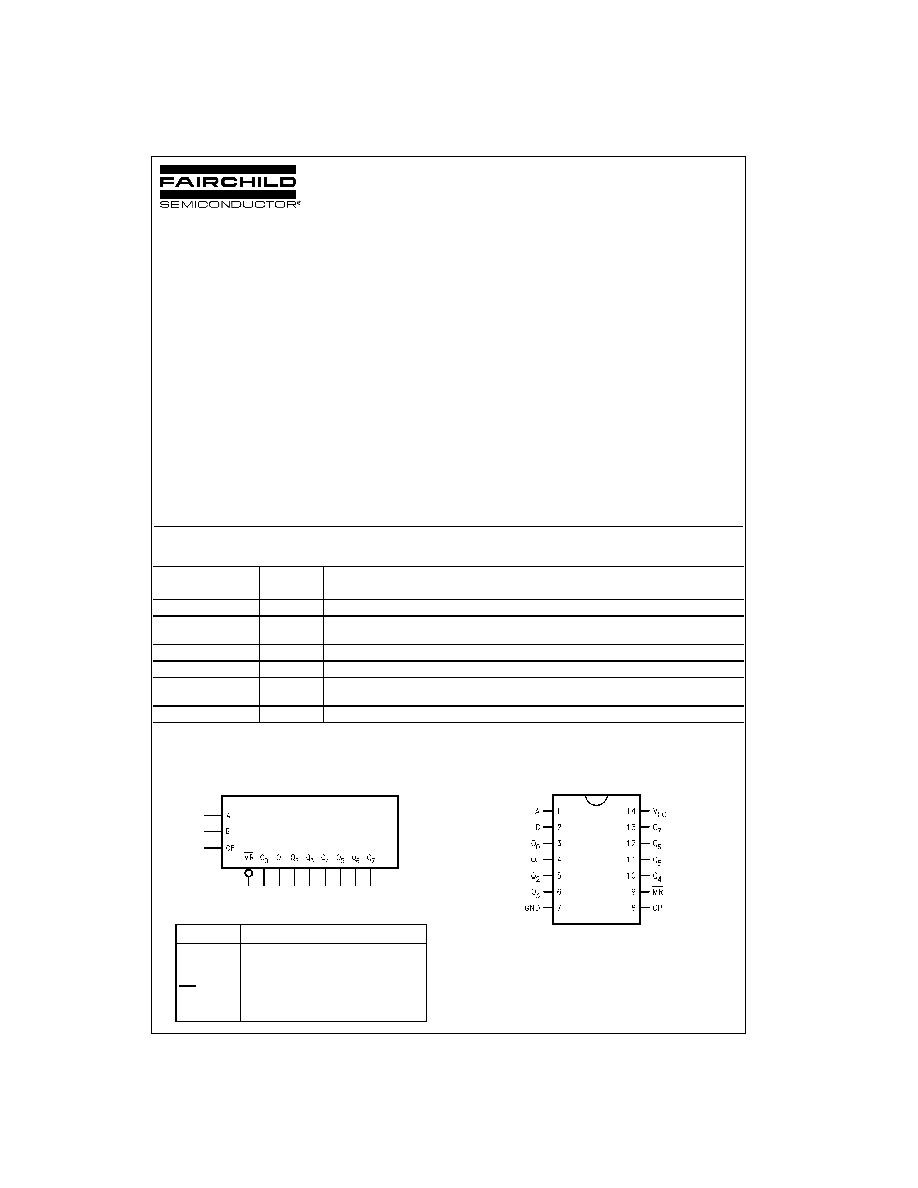
Logic Symbol
Pin Descriptions
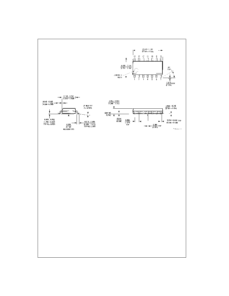
Connection Diagram
Order Number
Package
Package Description
Number
74VHC164M
M14A
14-Lead Small Outline Integrated Circuit (SOIC), JEDEC MS-012, 0.150" Narrow
74VHC164MX_NL
(Note 1)
M14A
Pb-Free 14-Lead Small Outline Integrated Circuit (SOIC), JEDEC MS-012, 0.150" Narrow
74VHC164SJ
M14D
Pb-Free 14-Lead Small Outline Package (SOP), EIAJ TYPE II, 5.3mm Wide
74VHC164MTC
MTC14
14-Lead Thin Shrink Small Outline Package (TSSOP), JEDEC MO-153, 4.4mm Wide
74VHC164MTCX_NL
(Note 1)
MTC14
Pb-Free 14-Lead Thin Shrink Small Outline Package (TSSOP), JEDEC MO-153, 4.4mm
Wide
74VHC164N
N14A
14-Lead Plastic Dual-In-Line Package (PDIP), JEDEC MS-001, 0.300" Wide
Pin Names
Description
A, B
Data Inputs
CP
Clock Pulse Input (Active Rising Edge)
MR
Master Reset Input (Active LOW)
Q
0
Q
7
Outputs
www.fairchildsemi.com
2
74
V
HC164
Functional Description
The VHC164 is an edge-triggered 8-bit shift register with
serial data entry and an output from each of the eight
stages. Data is entered serially through one of two inputs
(A or B); either of these inputs can be used as an active
High Enable for data entry through the other input. An
unused input must be tied HIGH.
Each LOW-to-HIGH transition on the Clock (CP) input
shifts data one place to the right and enters into Q
0
the log-
ical AND of the two data inputs (A · B) that existed before
the rising clock edge. A LOW level on the Master Reset
(MR) input overrides all other inputs and clears the register
asynchronously, forcing all Q outputs LOW.
Function Table
H
HIGH Voltage Levels
L
LOW Voltage Levels
X
Immaterial
Q
Lower case letters indicate the state of the referenced input or output
one setup time prior to the LOW-to-HIGH clock transition.
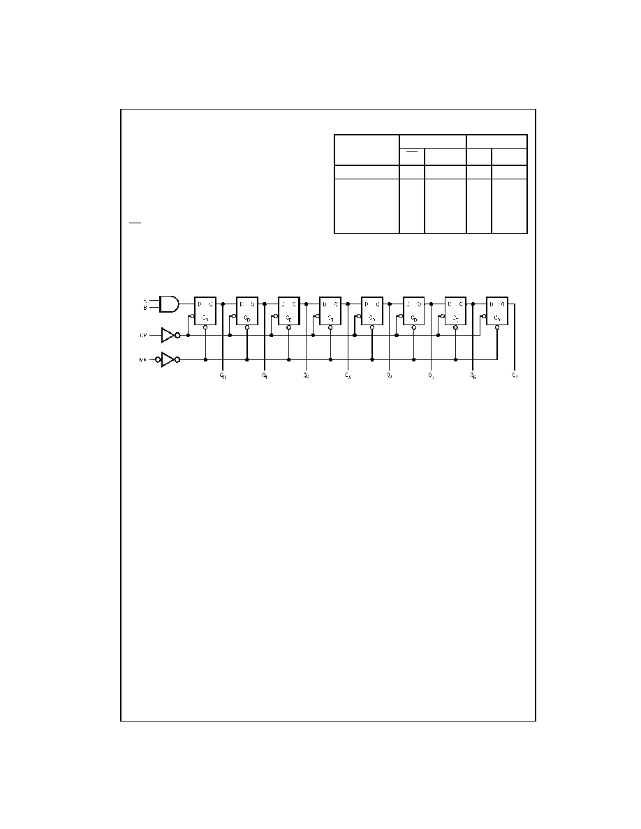
Logic Diagram
Please note that this diagram is provided only for the understanding of logic operations and should not be used to estimate propagation delays.
Operating
Inputs
Outputs
Mode
MR
A
B
Q
0
Q
1
Q
7
Reset (Clear)
L
X
X
L
LL
Shift
H
L
L
L
Q
0
Q
6
H
L
H
L
Q
0
Q
6
H
H
L
L
Q
0
Q
6
H
H
H
H
Q
0
Q
6
3
www.fairchildsemi.com
7
4
VH
C16
4
Absolute Maximum Ratings
(Note 2)
Recommended Operating
Conditions
(Note 3)
Note 2: Absolute maximum ratings are those values beyond which damage
to the device may occur. The databook specifications should be met, with-
out exception, to ensure that the system design is reliable over its power
supply, temperature, and output/input loading variables. Fairchild does not
recommend operation of circuits outside databook specifications.
Note 3: Unused inputs must be held HIGH or LOW. They may not float.
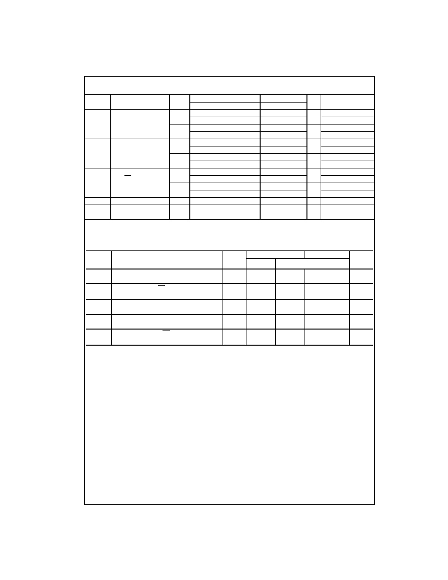
DC Electrical Characteristics
Noise Characteristics
Note 4: Parameter guaranteed by design.
Supply Voltage (V
CC
)
0.5V to
7.0V
DC Input Voltage (V
IN
)
0.5V to
7.0V
DC Output Voltage (V
OUT
)
0.5V to V
CC
0.5V
DC Diode Current (I
IK
)
20 mA
Output Diode Current (I
OK
)
r
20 mA
DC Output Current (I
OUT
)
r
25 mA
DC V
CC
/GND Current (I
CC
)
r
75 mA
Storage Temperature (T
STG
)
65
q
C to
150
q
C
Lead Temperature (T
L
)
(Soldering, 10 seconds)
260
q
C
Supply Voltage (V
CC
)
2.0V to 5.5V
Input Voltage (V
IN
)
0V to
5.5V
Output Voltage (V
OUT
)
0V to V
CC
Operating Temperature (T
OPR
)
40
q
C to
85
q
C
Input Rise and Fall Time (t
r
, t
f
)
V
CC
3.3V
r
0.3V
0 ns/V
a
100 ns/V
V
CC
5.0V
r
0.5V
0 ns/V
a
20 ns/V
Symbol
Parameter
V
CC
(V)
T
A
25
q
C
T
A
40
q
C to
85
q
C
Units
Conditions
Min
Typ
Max
Min
Max
V
IH
HIGH Level Input
2.0
1.50
1.50
V
Voltage
3.0
5.5
0.7 V
CC
0.7 V
CC
V
IL
LOW Level Input
2.0
0.50
0.50
V
Voltage
3.0
5.5
0.3 V
CC
0.3 V
CC
V
OH
HIGH Level Output
2.0
1.9
2.0
1.9
V
IN
V
IH
I
OH
50
P
A
Voltage
3.0
2.9
3.0
2.9
V
or V
IL
4.5
4.4
4.5
4.4
3.0
2.58
2.48
V
I
OH
4 mA
4.5
3.94
3.80
I
OH
8 mA
V
OL
LOW Level Output
2.0
0.0
0.1
0.1
V
IN
V
IH
I
OL
50
P
A
Voltage
3.0
0.0
0.1
0.1
V
or V
IL
4.5
0.0
0.1
0.1
3.0
0.36
0.44
V
I
OL
4 mA
4.5
0.36
0.44
I
OL
8 mA
I
IN
Input Leakage Current
0
5.5
r
0.1
r
1.0
P
A
V
IN
5.5V or GND
I
CC
Quiescent Supply Current
5.5
4.0
40.0
P
A
V
IN
V
CC
or GND
Symbol
Parameter
V
CC
T
A
25
q
C
Units
Conditions
(V)
Typ
Limits
V
OLP
Quiet Output Maximum
5.0
0.5
0.8
V
C
L
50 pF
(Note 4)
Dynamic V
OL
V
OLV
Quiet Output Minimum
5.0
0.5
0.8
V
C
L
50 pF
(Note 4)
Dynamic V
OL
V
IHD
Minimum HIGH Level
5.0
3.5
V
C
L
50 pF
(Note 4)
Dynamic Input Voltage
V
ILD
Maximum LOW Level
5.0
1.5
V
C
L
50 pF
(Note 4)
Dynamic Input Voltage
www.fairchildsemi.com
4
74
V
HC164
AC Electrical Characteristics
Note 5: C
PD
is defined as the value of the internal equivalent capacitance which is calculated from the operating current consumption without load. Average
operating current can be obtained from the equation: I
CC
(opr.)
C
PD
* V
CC
* f
IN
I
CC
.
AC Operating Requirements
Note 6: V
CC
is 3.3
r
0.3V or 5.0
r
0.5V
Symbol
Parameter
V
CC
(V)
T
A
25
q
C
T
A
40
q
C to
85
q
C
Units
Conditions
Min
Typ
Max
Min
Max
f
MAX
Maximum Clock Frequency
3.3
r
0.3
80
125
65
MHz
C
L
15 pF, R
L
1k
50
75
45
C
L
50 pF, R
L
1k
5.0
r
0.5
125
175
105
MHz
C
L
15 pF, R
L
1k
85
115
75
C
L
50 pF, R
L
1k
t
PLH
Propagation Delay
3.3
r
0.3
8.4
12.8
1.0
15.0
ns
C
L
15 pF, R
L
1k
t
PHL
Time (CPQ
n
)
10.9
16.3
1.0
18.5
C
L
50 pF, R
L
1k
5.0
r
0.5
5.8
9.0
1.0
10.5
ns
C
L
15 pF, R
L
1k
7.3
11.0
1.0
12.5
C
L
50 pF, R
L
1k
t
PHL
Propagation Delay
3.3
r
0.3
8.3
12.8
1.0
15.0
ns
C
L
15 pF, R
L
1k
Time (MRQ
n
)
10.8
16.3
1.0
18.5
C
L
50 pF, R
L
1k
5.0
r
0.5
5.2
8.6
1.0
10.0
ns
C
L
15 pF, R
L
1k
6.7
10.6
1.0
12.0
C
L
50 pF, R
L
1k
C
IN
Input Capacitance
4
10
10
pF
V
CC
Open
C
PD
Power Dissipation
76
pF
(Note 5)
Capacitance
Symbol
Parameter
V
CC
(V)
(Note 6)
T
A
25
q
C
T
A
40
q
C to
85
q
C
Units
Typ
Guaranteed Minimum
t
W
(L)
Minimum Pulse Width (CP)
3.3
5.0
5.0
ns
t
W
(H)
5.0
5.0
5.0
t
W
(L)
Minimum Pulse Width (MR)
3.3
5.0
5.0
ns
5.0
5.0
5.0
t
S
Minimum Setup Time
3.3
5.0
6.0
ns
5.0
4.5
4.5
t
H
Minimum Hold Time
3.3
0.0
0.0
ns
5.0
1.0
1.0
t
REC
Minimum Removal Time (MR)
3.3
2.5
2.5
ns
5.0
2.5
2.5