Äîêóìåíòàöèÿ è îïèñàíèÿ www.docs.chipfind.ru
April 1994
Revised April 1999
7
4
VH
C27
3
Oct
a
l D-T
ype Fli
p
-
F
lop
© 1999 Fairchild Semiconductor Corporation
DS011670.prf
www.fairchildsemi.com
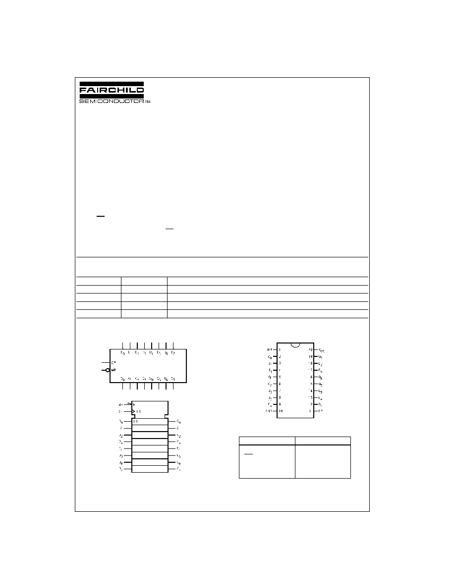
74VHC273
Octal D-Type Flip-Flop
General Description
The VHC273 is an advanced high speed CMOS Octal D-
type flip-flop fabricated with silicon gate CMOS technology.
It achieves the high speed operation similar to equivalent
Bipolar Schottky TTL while maintaining the CMOS low
power dissipation.
The register has a common buffered Clock (CP) which is
fully edge-triggered. The state of each D input, one setup
time before the LOW-to-HIGH clock transition, is trans-
ferred to the corresponding flip-flop's Q output. The Master
Reset (MR) input will clear all flip-flops simultaneously. All
outputs will be forced LOW independently of Clock or Data
inputs by a LOW voltage level on the MR input.
An input protection circuit insures that 0V to 7V can be
applied to the inputs pins without regard to the supply volt-
age. This device can be used to interface 5V to 3V systems
and two supply systems such as battery backup. This cir-
cuit prevents device destruction due to mismatched supply
and input voltages.
Features
s
High Speed: f
MAX
=
165 MHz (typ) at V
CC
=
5V
s
Low power dissipation: I
CC
=
4
µ
A (max) at T
A
=
25
°
C
s
High noise immunity: V
NIH
=
V
NIL
=
28% V
CC
(min)
s
Power down protection is provided on all inputs
s
Low noise: V
OLP
=
0.9V (max)
s
Pin and function compatible with 74HC273
Ordering Code:
Surface mount packages are also available on Tape and Reel. Specify by appending the suffix letter "X" to the ordering code.
Logic Symbols
IEEE/IEC
Connection Diagram
Pin Descriptions
Order Number
Package Number
Package Description
74VHC273M
M20B
20-Lead Small Outline Integrated Circuit (SOIC), JEDEC MS-013, 0.300 Wide
74VHC273SJ
M20D
20-Lead Small Outline Package (SOP), EIAJ TYPE II, 5.3mm Wide
74VHC273MTC
MTC20
20-Lead Thin Shrink Small Outline Package (TSSOP), JEDEC MO-153, 4.4mm Wide
74VHC273N
N20A
20-Lead Plastic Dual-In-Line Package (PDIP), JEDEC MS-001, 0.300 Wide
Pin Names
Description
D
0
D
7
Data Inputs
MR
Master Reset
CP
Clock Pulse Input
Q
0
Q
7
Data Outputs
www.fairchildsemi.com
2
74
V
HC273
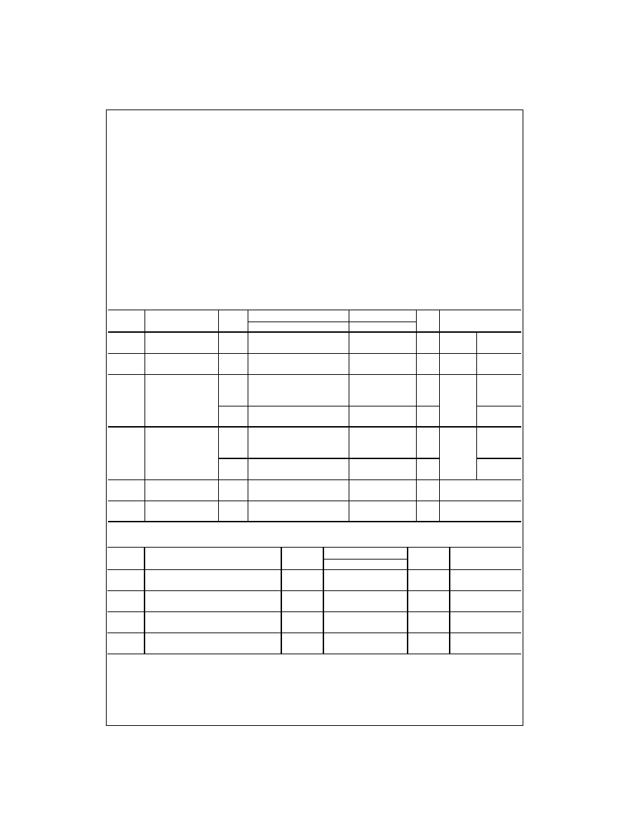
Function Table
H
=
HIGH Voltage Level
L
=
LOW Voltage Level
X
=
Immaterial
=
LOW-to-HIGH Transition
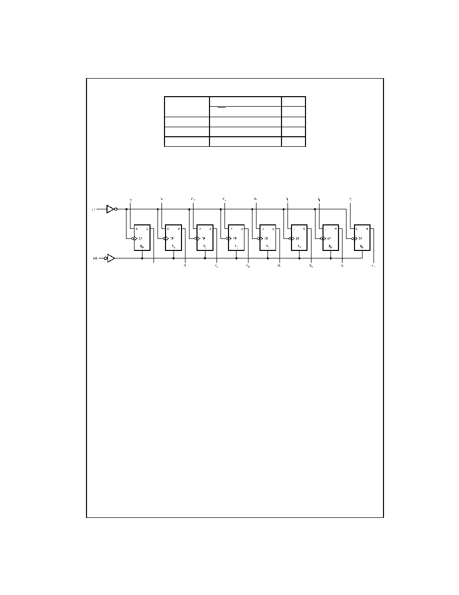
Logic Diagram
Please note that this diagram is provided only for the understanding of logic operations and should not be used to estimate propagation delays.
Operating Mode
Inputs
Outputs
MR
CP
D
n
Q
n
Reset (Clear)
L
X
X
L
Load '1'
H
H
H
Load '0'
H
L
L
3
www.fairchildsemi.com
7
4
VH
C27
3
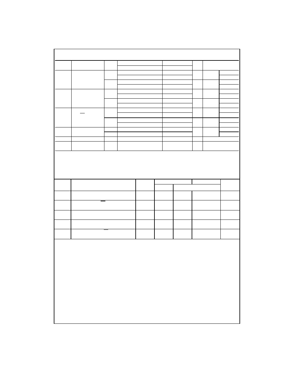
Absolute Maximum Ratings
(Note 1)
Recommended Operating
Conditions
(Note 2)
Note 1: Absolute Maximum Ratings are values beyond which the device
may be damaged or have its useful life impaired. The databook specifica-
tions should be met, without exception, to ensure that the system design is
reliable over its power supply, temperature, and output/input loading vari-
ables. Fairchild does not recommend operation outside databook specifica-
tions.
Note 2: Unused inputs must be held HIGH or LOW. They may not float.
DC Electrical Characteristics
Noise Characteristics
Note 3: Parameter guaranteed by design.
Supply Voltage (V
CC
)
-
0.5V to
+
7.0V
DC Input Voltage (V
IN
)
-
0.5V to
+
7.0V
DC Output Voltage (V
OUT
)
-
0.5V to V
CC
+
0.5V
Input Diode Current (I
IK
)
-
20 mA
Output Diode Current (I
OK
)
±
20 mA
DC Output Current (I
OUT
)
±
25 mA
DC V
CC
/GND Current (I
CC
)
±
75 mA
Storage Temperature (T
STG
)
-
65
°
C to
+
150
°
C
Lead Temperature (T
L
)
(Soldering, 10 seconds)
260
°
C
Supply Voltage (V
CC
)
2.0V to
+
5.5V
Input Voltage (V
IN
)
0V to
+
5.5V
Output Voltage (V
OUT
)
0V to V
CC
Operating Temperature (T
OPR
)
-
40
°
C to
+
85
°
C
Input Rise and Fall Time (t
r
, t
f
)
V
CC
=
3.3V
±
0.3V
0 ns/V
100 ns/V
V
CC
=
5.0V
±
0.5V
0 ns/V
20 ns/V
Symbol
Parameter
V
CC
(V)
T
A
=
25
°
C
T
A
=
-
40
°
C to
+
85
°
C
Units
Conditions
Min
Typ
Max
Min
Max
V
IH
HIGH Level Input
2.0
1.50
1.50
V
Voltage
3.0
-
5.5
0.7 V
CC
0.7 V
CC
V
IL
LOW Level Input
2.0
0.50
0.50
V
Voltage
3.0
-
5.5
0.3 V
CC
0.3 V
CC
V
OH
HIGH Level Output
2.0
1.9
2.0
1.9
V
V
IN
=
V
IH
I
OH
=
-
50
µ
A
Voltage
3.0
2.9
3.0
2.9
or V
IL
4.5
4.4
4.5
4.4
3.0
2.58
2.48
V
I
OH
=
-
4 mA
4.5
3.94
3.80
I
OH
=
-
8 mA
V
OL
LOW Level Output
2.0
0.0
0.1
0.1
V
V
IN
=
V
IH
I
OL
=
50
µ
A
Voltage
3.0
0.0
0.1
0.1
or V
IL
4.5
0.0
0.1
0.1
3.0
0.36
0.44
V
I
OL
=
4 mA
4.5
0.36
0.44
I
OL
=
8 mA
I
IN
Input Leakage
0
-
5.5
±
0.1
±
1.0
µ
A
V
IN
=
5.5V or GND
Current
I
CC
Quiescent Supply
5.5
4.0
40.0
µ
A
V
IN
=
V
CC
or GND
Current
Symbol
Parameter
V
CC
(V)
T
A
=
25
°
C
Units
Conditions
Typ
Limits
V
OLP
Quiet Output Maximum Dynamic V
OL
5.0
0.6
0.9
V
C
L
=
50 pF
(Note 3)
V
OLV
Quiet Output Minimum Dynamic V
OL
5.0
-
0.6
-
0.9
V
C
L
=
50 pF
(Note 3)
V
IHD
Minimum HIGH Level Dynamic Input Voltage
5.0
3.5
V
C
L
=
50 pF
(Note 3)
V
ILD
Maximum LOW Level Dynamic Input Voltage
5.0
1.5
V
C
L
=
50 pF
(Note 3)
www.fairchildsemi.com
4
74
V
HC273
AC Electrical Characteristics
Note 4: Parameter guaranteed by design t
OSLH
=
|t
PLH
max
-
t
PLH
min|; t
OSHL
=
|t
PHL
max
-
t
PHL
min|.
Note 5: C
PD
is defined as the value of the internal equivalent capacitance which is calculated from the operating current consumption without load. Average
operating current can be obtained from the equation: I
CC
(opr.)
=
C
PD
* V
CC
* f
IN
+
I
CC
/8 (per F/F). The total C
PD
when n pieces of the Flip Flop operates can
be calculated by the equation: C
PD
(total)
=
22
+
9n.
AC Operating Requirements
Note 6: V
CC
is 3.3
±
0.3V or 5.0
±
0.5V
Symbol
Parameter
V
CC
(V)
T
A
=
25
°
C
T
A
=
-
40
°
C to
+
85
°
C
Units
Conditions
Min
Typ
Max
Min
Max
f
MAX
Maximum Clock
3.3
±
0.3
75
120
65
MHz
C
L
=
15 pF
Frequency
50
75
45
C
L
=
50 pF
5.0
±
0.5
120
165
100
MHz
C
L
=
15 pF
80
110
70
C
L
=
50 pF
t
PLH
Propagation Delay
3.3
±
0.3
8.7
13.6
1.0
16.0
ns
C
L
=
15 pF
t
PHL
Time (CK - Q)
11.2
17.1
1.0
19.5
C
L
=
50 pF
5.0
±
0.5
5.8
9.0
1.0
10.5
ns
C
L
=
15 pF
7.3
11.0
1.0
12.5
C
L
=
50 pF
t
PHL
Propagation Delay
3.3
±
0.3
8.9
13.6
1.0
16.0
ns
C
L
=
15 pF
Time (MR - Q)
11.4
17.1
1.0
19.5
C
L
=
50 pF
5.0
±
0.5
5.2
8.5
1.0
10.0
ns
C
L
=
15 pF
6.7
10.5
1.0
12.0
C
L
=
50 pF
t
OSLH
Output to
3.3
±
0.3
1.5
1.5
ns
(Note 4)
C
L
=
50 pF
t
OSHL
Output Skew
5.0
±
0.5
1.0
1.0
C
L
=
50 pF
C
IN
Input Capacitance
4
10
10
pF
V
CC
=
Open
C
PD
Power Dissipation
31
pF
(Note 5)
Capacitance
Symbol
Parameter
V
CC
(V)
(Note 6)
T
A
=
25
°
C
T
A
=
-
40
°
C to
+
85
°
C
Units
Typ
Guaranteed Minimum
t
W
(L)
Minimum Pulse Width (CK)
3.3
5.5
6.5
ns
t
W
(H)
5.0
5.0
5.0
t
W
(L)
Minimum Pulse Width (MR)
3.3
5.0
6.0
ns
5.0
5.0
5.0
t
S
Minimum Setup Time
3.3
5.5
6.5
ns
5.0
4.5
4.5
t
H
Minimum Hold Time
3.3
1.0
1.0
ns
5.0
1.0
1.0
t
REC
Minimum Removal Time (MR)
3.3
2.5
2.5
ns
5.0
2.0
2.0
5
www.fairchildsemi.com
7
4
VH
C27
3
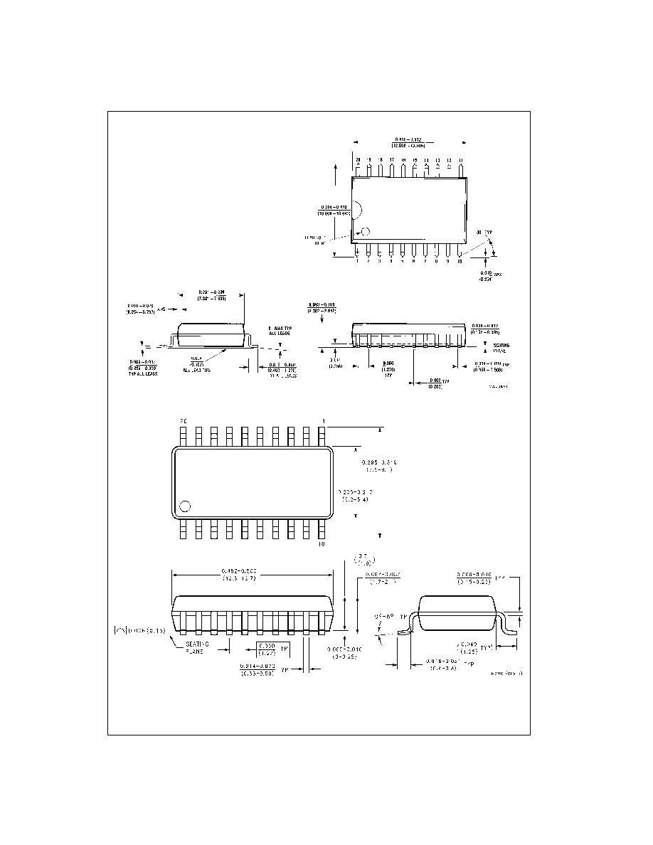
Physical Dimensions
inches (millimeters) unless otherwise noted
20-Lead Small Outline Integrated Circuit (SOIC), JEDEC MS-013, 0.300 Wide
Package Number M20B
20-Lead Small Outline Package (SOP), EIAJ TYPE II, 5.3mm Wide
Package Number M20D