Äîêóìåíòàöèÿ è îïèñàíèÿ www.docs.chipfind.ru
© 2005 Fairchild Semiconductor Corporation
DS011565
www.fairchildsemi.com
March 1993
Revised May 2005
7
4
VH
C57
4
Oct
a
l
D-
T
ype Fl
ip
-Fl
op wi
th
3-ST
A
T
E Out
put
s
74VHC574
Octal D-Type Flip-Flop with 3-STATE Outputs
General Description
The VHC574 is an advanced high speed CMOS octal flip-
flop with 3-STATE output fabricated with silicon gate CMOS
technology. It achieves the high speed operation similar to
equivalent Bipolar Schottky TTL while maintaining the
CMOS low power dissipation. This 8-bit D-type flip-flop is
controlled by a clock input (CP) and an output enable input
(OE). When the OE input is HIGH, the eight outputs are in
a high impedance state.
An input protection circuit ensures that 0V to 7V can be
applied to the input pins without regard to the supply volt-
age. This device can be used to interface 5V to 3V systems
and two supply systems such as battery back up. This cir-
cuit prevents device destruction due to mismatched supply
and input voltages.
Features
s
High Speed: t
PD
5.6 ns (typ) at V
CC
5V
s
High Noise Immunity: V
NIH
V
NIL
28% V
CC
(Min)
s
Power Down Protection is provided on all inputs
s
Low Noise: V
OLP
0.6V (typ)
s
Low Power Dissipation: I
CC
4
P
A (Max) @ T
A
25
q
C
s
Pin and Function Compatible with 74HC574
Ordering Code:
Surface mount packages are also available on Tape and Reel. Specify by appending the suffix letter "X" to the ordering code.
Pb-Free package per JEDEC J-STD-020B.
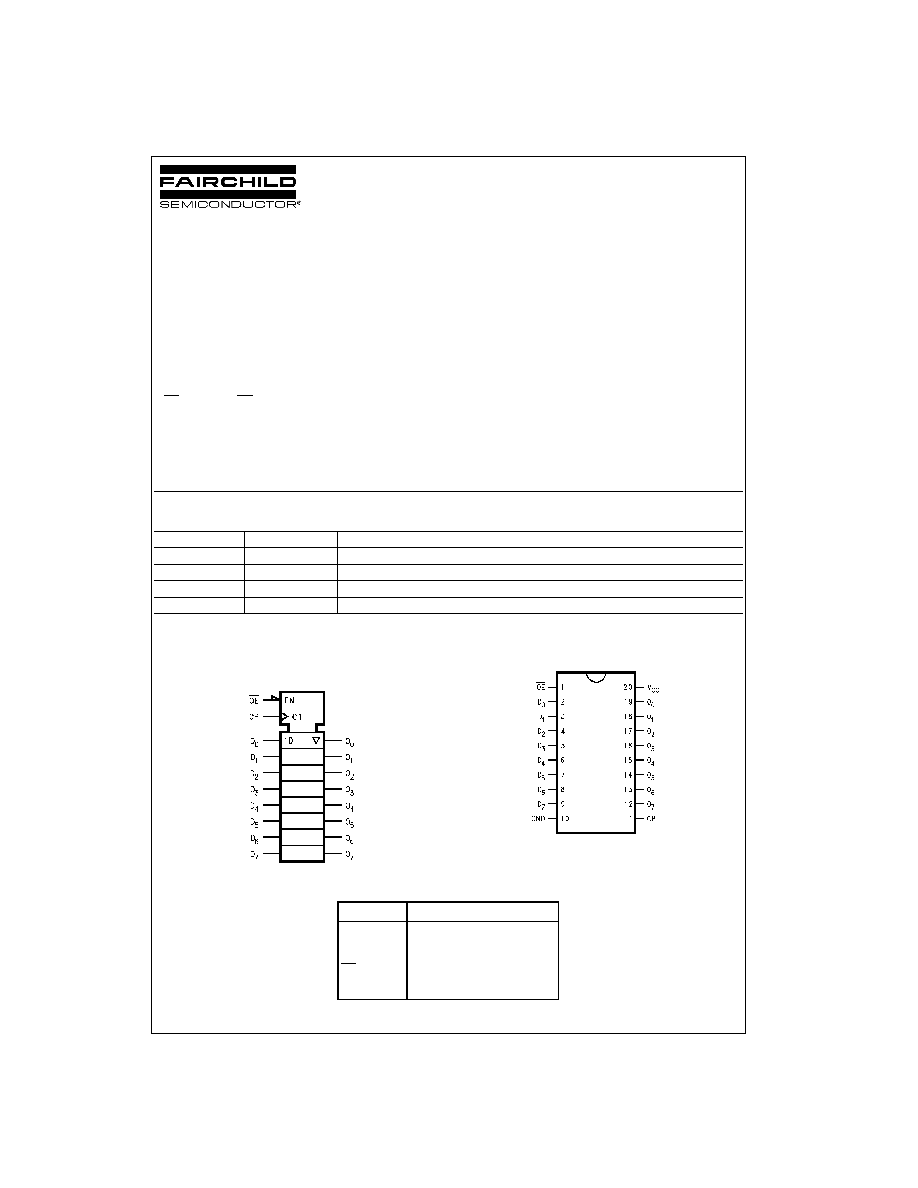
Logic Symbol
IEEE/IEC
Connection Diagram
Pin Descriptions
Order Number
Package Number
Package Description
74VHC574M
M20B
20-Lead Small Outline Integrated Circuit (SOIC), JEDEC MS-013, 0.300" Wide
74VHC574SJ
M20D
Pb-Free 20-Lead Small Outline Package (SOP), EIAJ TYPE II, 5.3mm Wide
74VHC574MTC
MTC20
20-Lead Thin Shrink Small Outline Package (TSSOP), JEDEC MO-153, 4.4mm Wide
74VHC574N
N20A
20-Lead Plastic Dual-In-Line Package (PDIP), JEDEC MS-001, 0.300" Wide
Pin Names
Description
D
0
D
7
Data Inputs
CP
Clock Pulse Input
OE
3-STATE Output Enable Input
O
0
O
7
3-STATE Outputs
www.fairchildsemi.com
2
74
V
HC574
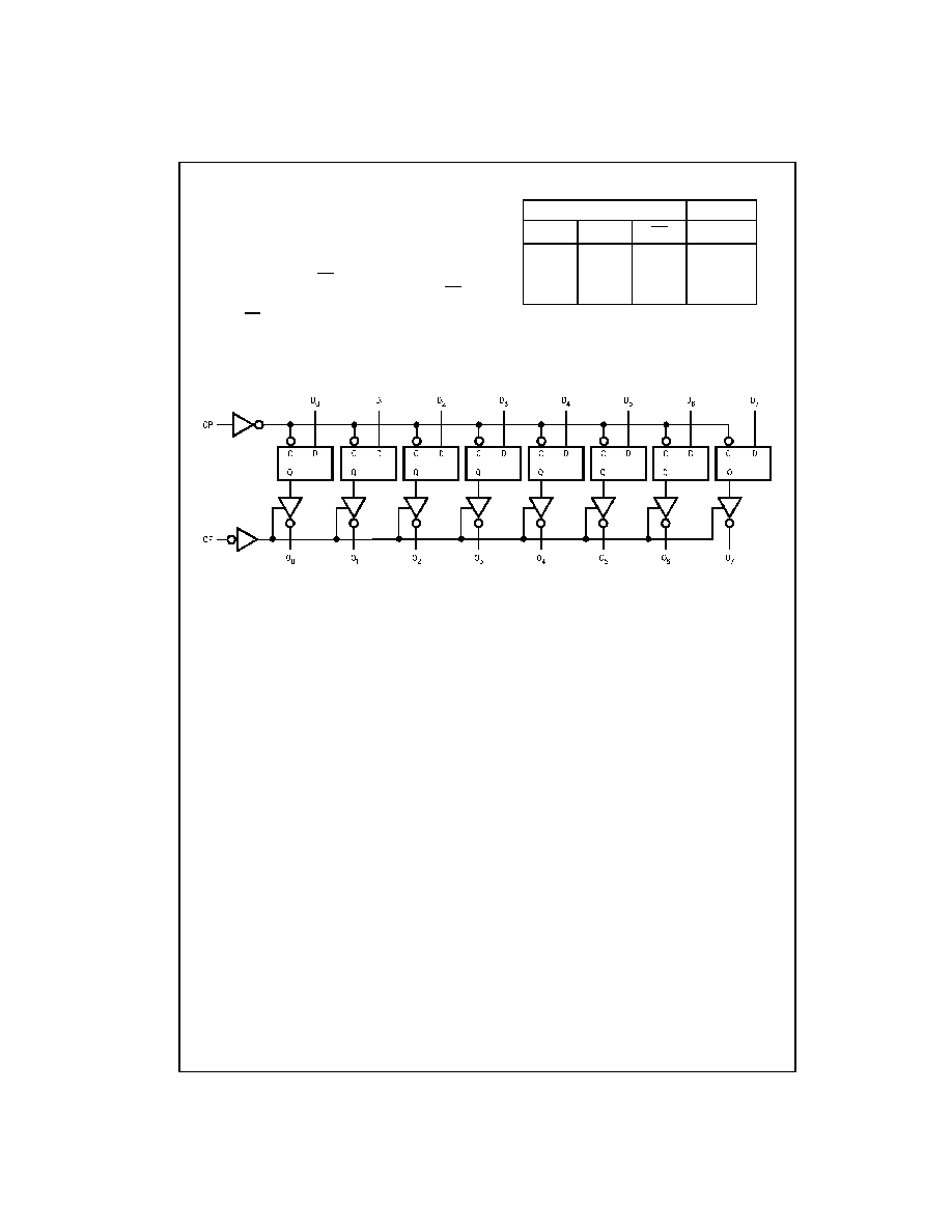
Functional Description
The VHC574 consists of eight edge-triggered flip-flops with
individual D-type inputs and 3-STATE true outputs. The
buffered clock and buffered Output Enable are common to
all flip-flops. The eight flip-flops will store the state of their
individual D inputs that meet the setup and hold time
requirements on the LOW-to-HIGH Clock (CP) transition.
With the Output Enable (OE) LOW, the contents of the
eight flip-flops are available at the outputs. When the OE is
HIGH, the outputs go to the high impedance state. Opera-
tion of the OE input does not affect the state of the flip-
flops.
Truth Table
H
HIGH Voltage Level
L
LOW Voltage Level
X
Immaterial
Z
High Impedance
LOW-to-HIGH Transition
Logic Diagram
Please note that this diagram is provided only for the understanding of logic operations and should not be used to estimate propagation delays.
Inputs
Outputs
D
n
CP
OE
O
n
H
L
H
L
L
L
X
X
H
Z
3
www.fairchildsemi.com
7
4
VH
C57
4
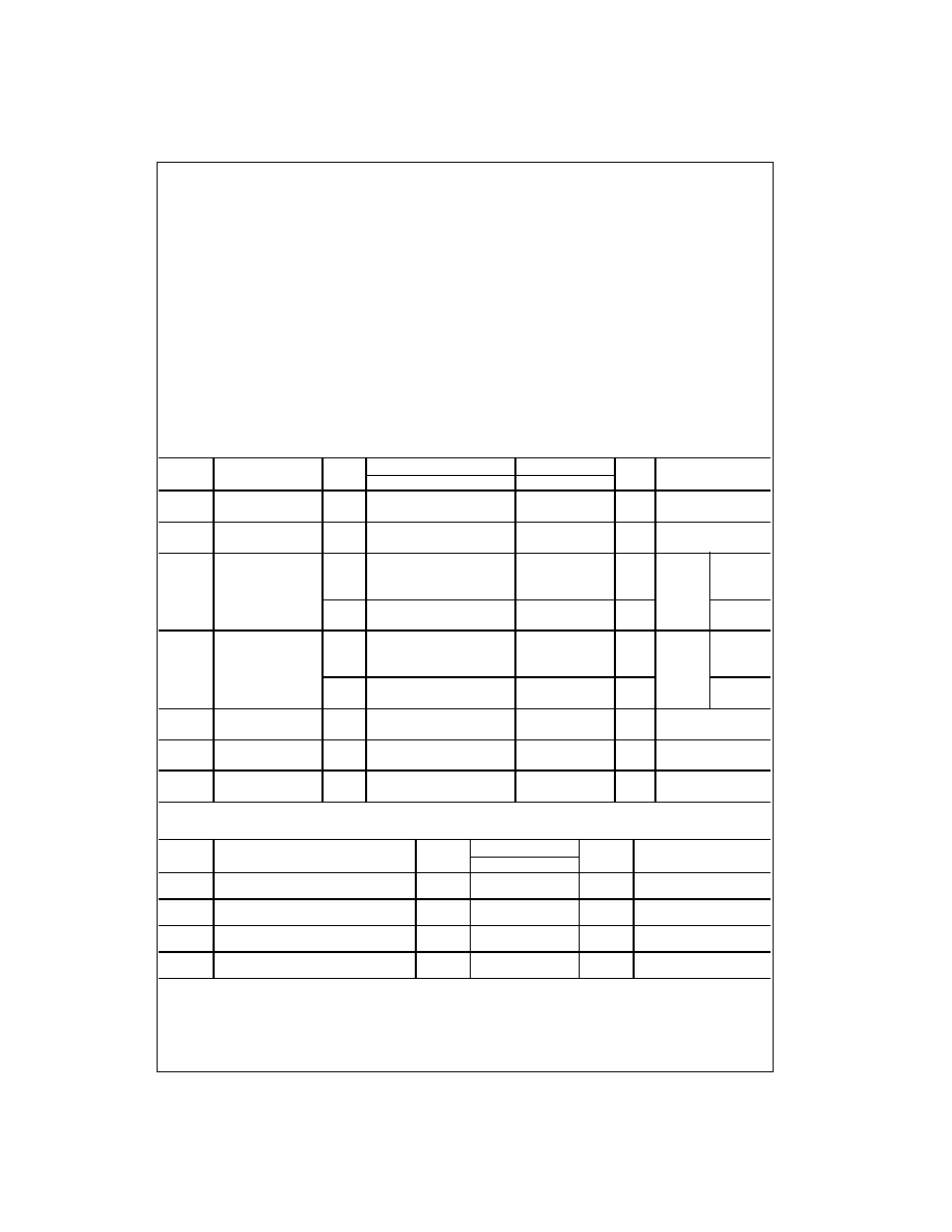
Absolute Maximum Ratings
(Note 1)
Recommended Operating
Conditions
(Note 2)
Note 1: Absolute Maximum Ratings are values beyond which the device
may be damaged or have its useful life impaired. The databook specifica-
tions should be met, without exception, to ensure that the system design is
reliable over its power supply, temperature, and output/input loading vari-
ables. Fairchild does not recommend operation outside databook specifica-
tions.
Note 2: Unused inputs must be held HIGH or LOW. They may not float.
DC Electrical Characteristics
Noise Characteristics
Note 3: Parameter guaranteed by design.
Supply Voltage (V
CC
)
0.5V to
7.0V
DC Input Voltage (V
IN
)
0.5V to
7.0V
DC Output Voltage (V
OUT
)
0.5V to V
CC
0.5V
Input Diode Current (I
IK
)
20 mA
Output Diode Current
r
20 mA
DC Output Current (I
OUT
)
r
25 mA
DC V
CC
/GND Current (I
CC
)
r
75 mA
Storage Temperature (T
STG
)
65
q
C to
150
q
C
Lead Temperature (T
L
)
(Soldering, 10 seconds)
260
q
C
Supply Voltage (V
CC
)
2.0V to
5.5V
Input Voltage (V
IN
)
0V to
5.5V
Output Voltage (V
OUT
)
0V to V
CC
Operating Temperature (T
OPR
)
40
q
C to
85
q
C
Input Rise and Fall Time (t
r
, t
f
)
V
CC
3.3V
r
0.3V
0
a
100 ns/V
V
CC
5.0V
r
0.5V
0
a
20 ns/V
Symbol
Parameter
V
CC
(V)
T
A
25
q
C
T
A
40
q
C to
85
q
C
Units
Conditions
Min
Typ
Max
Min
Max
V
IH
HIGH Level
2.0
1.50
1.50
V
Input Voltage
3.0
5.5
0.7 V
CC
0.7 V
CC
V
IL
LOW Level
2.0
0.50
0.50
V
Input Voltage
3.0
5.5
0.3 V
CC
0.3 V
CC
V
OH
HIGH Level
2.0
1.9
2.0
1.9
V
IN
V
IH
I
OH
50
P
A
Output Voltage
3.0
2.9
3.0
2.9
V
or V
IL
4.5
4.4
4.5
4.4
3.0
2.58
2.48
V
I
OH
4 mA
4.5
3.94
3.80
I
OH
8 mA
V
OL
LOW Level
2.0
0.0
0.1
0.1
V
IN
V
IH
I
OL
50
P
A
Output Voltage
3.0
0.0
0.1
0.1
V
or V
IL
4.5
0.0
0.1
0.1
3.0
0.36
0.44
V
I
OL
4 mA
4.5
0.36
0.44
I
OL
8 mA
I
OZ
3-STATE 5.5
r
0.25
r
2.5
P
A
V
IN
V
IH
or V
IL
Output Off-State Current
V
OUT
V
CC
or GND
I
IN
Input Leakage
0
5.5
r
0.1
r
1.0
P
A
V
IN
5.5V or GND
Current
I
CC
Quiescent Supply
5.5
4.0
40.0
P
A
V
IN
V
CC
or GND
Current
Symbol
Parameter
V
CC
(V)
T
A
25
q
C
Units
Conditions
Typ
Limits
V
OLP
(Note 3)
Quiet Output Maximum Dynamic V
OL
5.0
1.0
1.2
V
C
L
50 pF
V
OLV
(Note 3)
Quiet Output Minimum Dynamic V
OL
5.0
0.8
1.0
V
C
L
50 pF
V
IHD
(Note 3)
Minimum HIGH Level Dynamic Input Voltage
5.0
3.5
V
C
L
50 pF
V
ILD
(Note 3)
Maximum LOW Level Dynamic Input Voltage
5.0
1.5
V
C
L
50 pF
www.fairchildsemi.com
4
74
V
HC574
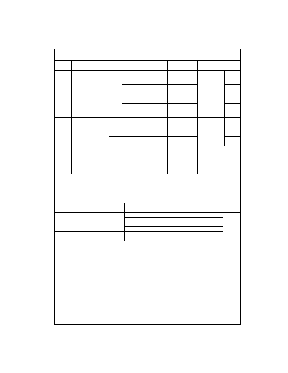
AC Electrical Characteristics
Note 4: Parameter guaranteed by design. t
OSLH
|t
PLH max
t
PLH min
|; t
OSHL
|t
PHL max
t
PHL min
|
Note 5: C
PD
is defined as the value of the internal equivalent capacitance which is calculated from the operating current consumption without load. Average
operating current can be obtained by the equation: I
CC
(opr.)
C
PD
* V
CC
* f
IN
I
CC
/8 (per F/F). The total C
PD
when n pcs. of the Octal D Flip-Flop operates
can be calculated by the equation: C
PD
(total)
20
8n.
AC Operating Requirements
Symbol
Parameter
V
CC
(V)
T
A
25
q
C
T
A
40
q
C to
85
q
C
Units
Conditions
Min
Typ
Max
Min
Max
t
PLH
Propagation Delay
3.3
r
0.3
8.5
13.2
1.0
15.5
ns
C
L
15 pF
t
PHL
Time (CP to O
n
)
11.0
16.7
1.0
19.0
C
L
50 pF
5.0
r
0.5
5.6
8.6
1.0
10.0
ns
C
L
15 pF
7.1
10.6
1.0
12.0
C
L
50 pF
t
PZL
3-STATE Output
3.3
r
0.3
8.2
12.8
1.0
15.0
ns
R
L
1 k
:
C
L
15 pF
t
PZH
Enable Time
10.7
16.3
1.0
18.5
C
L
50 pF
5.0
r
0.5
5.9
9.0
1.0
10.5
ns
C
L
15 pF
7.4
11.0
1.0
12.5
C
L
50 pF
t
PLZ
3-STATE Output
3.3
r
0.3
11.0
15.0
1.0
17.0
ns
R
L
1 k
:
C
L
50 pF
t
PHZ
Disable Time
5.0
r
0.5
7.1
10.1
1.0
11.5
C
L
50 pF
t
OSLH
Output to
3.3
r
0.3
1.5
1.5
ns
(Note 4)
C
L
50 pF
t
OSHL
Output Skew
5.0
r
0.5
1.0
1.0
C
L
50 pF
f
MAX
Maximum Clock
3.3
r
0.3
80
125
65
MHz
C
L
15 pF
Frequency
50
75
45
C
L
50 pF
5.0
r
0.5
130
180
110
C
L
15 pF
85
115
75
C
L
50 pF
C
IN
Input
4
10
10
pF
V
CC
Open
Capacitance
C
OUT
Output
6
pF
V
CC
5.0V
Capacitance
C
PD
Power Dissipation
28
pF
(Note 5)
Capacitance
Symbol
Parameter
V
CC
(V)
T
A
25
q
C
T
A
40
q
C to
85
q
C
Units
Min
Typ
Max
Min
Max
t
W
(H)
Minimum Pulse Width (CP)
3.3
r
0.3
5.0
5.0
ns
t
W
(L)
5.0
r
0.5
5.0
5.0
t
S
Minimum Set-Up Time
3.3
r
0.3
3.5
3.5
ns
5.0
r
0.5
3.5
3.5
t
H
Minimum Hold Time
3.3
r
0.3
1.5
1.5
5.0
r
0.5
1.5
1.5
5
www.fairchildsemi.com
7
4
VH
C57
4
Physical Dimensions
inches (millimeters) unless otherwise noted
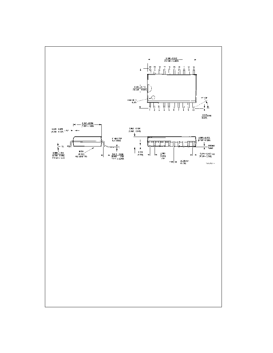
20-Lead Small Outline Integrated Circuit (SOIC), JEDEC MS-013, 0.300" Wide
Package Number M20B