
December 1998
Revised March 1999
7
4
VH
CT1
4
A
Hex Schm
i
t
t
I
nver
ter
© 1999 Fairchild Semiconductor Corporation
DS500147.prf
www.fairchildsemi.com
74VHCT14A
Hex Schmitt Inverter
General Description
The VHCT14A is an advanced high speed CMOS Hex
Schmitt Inverter fabricated with silicon gate CMOS technol-
ogy. The VHCT14A contains six independent inverters
which are capable of transforming slowly changing input
signals into sharply defined, jitter-free output signals.
Protection circuits ensure that 0V to 7V can be applied to
the input pins without regard to the supply voltage and to
the output pins with V
CC
=
0V. These circuits prevent
device destruction due to mismatched supply and input/
output voltages. This device can be used to interface 3V to
5V systems and two supply systems such as battery
backup.
Features
s
High speed: t
PD
=
5.0 ns (typ) at T
A
=
25
∞
C
s
High noise immunity: V
IH
=
2.0V, V
IL
=
0.8V
s
Power down protection is provided on all inputs and out-
puts
s
Low noise: V
OLP
=
1.0V (max)
s
Low power dissipation:
I
CC
=
2
µ
A (max) @ T
A
=
25
∞
C
s
Pin and function compatible with 74HCT14
Ordering Code:
Surface mount packages are also available on Tape and Reel. Specify by appending the suffix letter "X" to the ordering code.
Logic Symbol
Pin Descriptions
Connection Diagram
Truth Table
Order Number
Package Number
Package Description
74VHCT14AM
M14A
14-Lead Small Outline Integrated Circuit (SOIC), JEDEC MS-120, 0.150" Narrow
74VHCT14ASJ
M14D
14-Lead Small Outline Package (SOP), EIAJ TYPE II, 5.3mm Wide
74VHCT14AMTC
MTC14
14-Lead Thin Shrink Small Outline Package (TSSOP), JEDEC MO-153, 4.4mm Wide
74VHCT14AN
N14A
14-Lead Plastic Dual-In-Line Package (PDIP), JEDEC MS-001, 0.300" Wide
Pin Names
Description
A
n
Inputs
O
n
Outputs
A
O
L
H
H
L

www.fairchildsemi.com
2
74VHC
T1
4A
Absolute Maximum Ratings
(Note 1)
Recommended Operating
Conditions
(Note 5)
Note 1: Absolute Maximum Ratings are values beyond which the device
may be damaged or have its useful life impaired. The databook specifica-
tions should be met, without exception, to ensure that the system design is
reliable over its power supply, temperature, and output/input loading vari-
ables. Fairchild does not recommend operation outside databook specifica-
tions.
Note 2: HIGH or LOW state. I
OUT
absolute maximum rating must be
observed.
Note 3: V
CC
=
0V.
Note 4: V
OUT
<
GND, V
OUT
>
V
CC
(Outputs Active)
Note 5: Unused inputs must be held HIGH or LOW. They may not float.
DC Electrical Characteristics
Noise Characteristics
Note 6: Parameter guaranteed by design.
Supply Voltage (V
CC
)
-
0.5V to
+
7.0V
DC Input Voltage (V
IN
)
-
0.5V to
+
7.0V
DC Output Voltage (V
OUT
)
(Note
2)
-
0.5V to V
CC
+
0.5V
(Note
3)
-
0.5V to 7.0V
Input Diode Current (I
IK
)
-
20 mA
Output Diode Current (I
OK
)
(Note 4)
±
20 mA
DC Output Current (I
OUT
)
±
25 mA
DC V
CC
/GND Current (I
CC
)
±
50 mA
Storage Temperature (T
STG
)
-
65
∞
C to
+
150
∞
C
Lead Temperature (T
L
)
(Soldering, 10 seconds)
260
∞
C
Supply Voltage (V
CC
)
4.5V to
+
5.5V
Input Voltage (V
IN
)
0V to
+
5.5V
Output Voltage (V
OUT
)
(Note 2)
0V to V
CC
(Note 3)
0V to 5.5V
Operating Temperature (T
OPR
)
-
40
∞
C to
+
85
∞
C
Symbol
Parameter
V
CC
(V)
T
A
=
25
∞
C
T
A
=
-
40
∞
C to
+
85
∞
C
Units
Conditions
Min
Typ
Max
Min
Max
V
P
Positive Threshold Voltage
4.5
1.9
1.9
V
5.5
2.1
2.1
V
N
Negative Threshold Voltage
4.5
0.5
0.5
V
5.5
0.6
0.6
V
H
Hysteresis Voltage
4.5
0.4
1.4
0.4
1.4
V
5.5
0.4
1.5
0.4
1.5
V
OH
HIGH Level Output Voltage
4.5
4.40
4.50
4.40
V
V
IN
=
V
IL
I
OH
=
-
50
µ
A
3.94
3.80
V
I
OH
=
-
8 mA
V
OL
LOW Level Output Voltage
4.5
0.0
0.1
0.1
V
V
IN
=
V
IH
I
OL
=
50
µ
A
0.36
0.44
V
I
OL
=
8 mA
I
IN
Input Leakage Current
0
-
5.5
±
0.1
±
1.0
µ
A
V
IN
=
5.5V or GND
I
CC
Quiescent Supply Current
5.5
2.0
20.0
µ
A
V
IN
=
V
CC
or GND
I
CCT
Maximum I
CC
/Input
5.5
1.35
1.50
mA
V
IN
=
3.4V
Other Inputs
=
V
CC
or GND
I
OFF
Output Leakage Current
0.0
0.5
5.0
µ
A
V
OUT
=
5.5V
(Power Down State)
Symbol
Parameter
V
CC
(V)
T
A
=
25
∞
C
Units
Conditions
Typ
Limits
V
OLP
(Note 6)
Quiet Output Maximum Dynamic V
OL
5.0
0.8
1.0
V
C
L
=
50 pF
V
OLV
(Note 6)
Quiet Output Minimum Dynamic V
OL
5.0
-
0.8
1.0
V
C
L
=
50 pF
V
IHD
(Note 6)
Minimum HIGH Level Dynamic Input Voltage
5.0
2.0
V
C
L
=
50 pF
V
ILD
(Note 6)
Maximum LOW Level Dynamic Input Voltage
5.0
0.8
V
C
L
=
50 pF

3
www.fairchildsemi.com
7
4
VH
CT1
4
A
AC Electrical Characteristics
Note 7: C
PD
is defined as the value of the internal equivalent capacitance which is calculated from the operating current consumption without load. Average
operating current can be obtained by the equation: I
CC
(opr.)
=
C
PD
* V
CC
* f
IN
+
I
CC
/6 (per gate).
Symbol
Parameter
V
CC
T
A
=
25
∞
C
T
A
=
-
40
∞
C to
+
85
∞
C
Units Conditions
(V)
Min
Typ
Max
Min
Max
t
PHL
Propagation Delay
5.0
±
0.5
5.0
7.6
1.0
9.0
ns
C
L
=
15 pF
t
PLH
6.5
9.6
1.0
11.0
ns
C
L
=
50 pF
C
IN
Input Capacitance
2
10
10
pF
V
CC
=
OPEN
C
PD
Power Dissipation Capacitance
11
pF
(Note 7)
www.fairchildsemi.com
4
74VHC
T1
4A
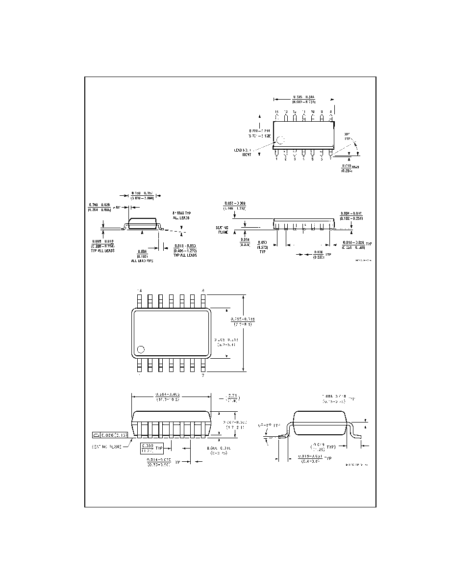
Physical Dimensions
inches (millimeters) unless otherwise noted
14-Lead Small Outline Integrated Circuit (SOIC), JEDEC MS-120, 0.150" Narrow
Package Number M14A
14-Lead Small Outline Package (SOP), EIAJ TYPE II, 5.3mm Wide
Package Number M14D

5
www.fairchildsemi.com
7
4
VH
CT1
4
A
Physical Dimensions
inches (millimeters) unless otherwise noted (Continued)
14-Lead Thin Shrink Small Outline Package (TSSOP), JEDEC MO-153, 4.4mm Wide
Package Number MTC14