
BC547 / BC547A / BC547B / BC547C
Discrete POWER & Signal
Technologies
NPN General Purpose Amplifier
BC547
BC547A
BC547B
BC547C
This device is designed for use as general purpose amplifiers
and switches requiring collector currents to 300 mA. Sourced from
Process 10. See PN100A for characteristics.
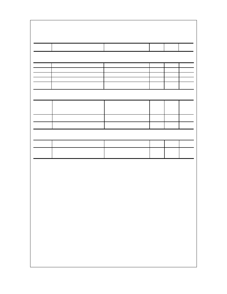
Absolute Maximum Ratings*
TA = 25∞C unless otherwise noted
*
These ratings are limiting values above which the serviceability of any semiconductor device may be impaired.
NOTES:
1) These ratings are based on a maximum junction temperature of 150 degrees C.
2) These are steady state limits. The factory should be consulted on applications involving pulsed or low duty cycle operations.
Thermal Characteristics
TA = 25∞C unless otherwise noted
Symbol
Parameter
Value
Units
V
CEO
Collector-Emitter Voltage
45
V
V
CES
Collector-Base Voltage
50
V
V
EBO
Emitter-Base Voltage
6.0
V
I
C
Collector Current - Continuous
500
mA
T
J
, T
stg
Operating and Storage Junction Temperature Range
-55 to +150
∞
C
Symbol
Characteristic
Max
Units
BC547 / A / B / C
P
D
Total Device Dissipation
Derate above 25
∞
C
625
5.0
mW
mW/
∞
C
R
JC
Thermal Resistance, Junction to Case
83.3
∞
C/W
R
JA
Thermal Resistance, Junction to Ambient
200
∞
C/W
E
B
C
TO-92
©
1997 Fairchild Semiconductor Corporation
547ABC, Rev B
BC547 / BC547A / BC547B / BC547C
NPN General Purpose Amplifier
(continued)
Electrical Characteristics
TA = 25∞C unless otherwise noted
OFF CHARACTERISTICS
Symbol
Parameter
Test Conditions
Min
Max
Units
V
(BR)CEO
Collector-Emitter Breakdown Voltage
I
C
= 1.0 mA, I
B
= 0
45
V
V
(BR)CBO
Collector-Base Breakdown Voltage
I
C
= 10
µ
A, I
E
= 0
50
V
V
(BR)CES
Collector-Base Breakdown Voltage
I
C
= 10
µ
A, I
E
= 0
50
V
V
(BR)EBO
Emitter-Base Breakdown Voltage
I
E
= 10
µ
A, I
C
= 0
6.0
V
I
CBO
Collector Cutoff Current
V
CB
= 30 V, I
E
= 0
V
CB
= 30 V, I
E
= 0, T
A
= +150
∞
C
15
5.0
nA
µ
A
ON CHARACTERISTICS
h
FE
DC Current Gain
V
CE
= 5.0 V, I
C
= 2.0 mA
547
547A
547B
547C
110
110
200
420
800
220
450
800
V
CE(
sat
)
Collector-Emitter Saturation Voltage
I
C
= 10 mA, I
B
= 0.5 mA
I
C
= 100 mA, I
B
= 5.0 mA
0.25
0.60
V
V
V
BE(
on
)
Base-Emitter On Voltage
V
CE
= 5.0 V, I
C
= 2.0 mA
V
CE
= 5.0 V, I
C
= 10 mA
0.58
0.70
0.77
V
V
SMALL SIGNAL CHARACTERISTICS
h
fe
Small-Signal Current Gain
I
C
= 2.0 mA, V
CE
= 5.0 V,
f = 1.0 kHz
125
900
NF
Noise Figure
V
CE
= 5.0 V, I
C
= 200
µ
A,
R
S
= 2.0 k
, f = 1.0 kHz,
B
W
= 200 Hz
10
dB