 | –≠–ª–µ–∫—Ç—Ä–æ–Ω–Ω—ã–π –∫–æ–º–ø–æ–Ω–µ–Ω—Ç: CD4016BCM | –°–∫–∞—á–∞—Ç—å:  PDF PDF  ZIP ZIP |
November 1983
Revised January 1999
CD401
6BC
Quad
Bi
la
ter
a
l Sw
i
t
c
h
© 1999 Fairchild Semiconductor Corporation
DS005661.prf
www.fairchildsemi.com
CD4016BC
Quad Bilateral Switch
General Description
The CD4016BC is a quad bilateral switch intended for the
transmission or multiplexing of analog or digital signals. It is
pin-for-pin compatible with CD4066BC.
Features
s
Wide supply voltage range: 3V to 15V
s
Wide range of digital and analog switching:
±
7.5 V
PEAK
s
"ON" resistance for 15V operation: 400
(typ.)
s
Matched "ON" resistance over 15V signal input:
R
ON
=
10
(typ.)
s
High degree of linearity:
0.4% distortion (typ.)
@ f
IS
=
1 kHz, V
IS
=
5 V
p-p
,
V
DD
-
V
SS
=
10V, R
L
=
10 k
s
Extremely low "OFF" switch leakage:
0.1 nA (typ.)
@ V
DD
-
V
SS
=
10V
T
A
=
25
∞
C
s
Extremely high control input impedance: 10
12
(typ.)
s
Low crosstalk between switches:
-
50 dB (typ.)
@ f
IS
=
0.9 MHz, R
L
=
1 k
s
Frequency response, switch "ON": 40 MHz (typ.)
Applications
∑ Analog signal switching/multiplexing
Signal gating
Squelch control
Chopper
Modulator/Demodulator
Commutating switch
∑ Digital signal switching/multiplexing
∑ CMOS logic implementation
∑ Analog-to-digital/digital-to-analog conversion
∑ Digital control of frequency, impedance, phase, and ana-
log-signal gain
Ordering Code:
Devices also available in Tape and Reel. Specify by appending the letter suffix "X" to the ordering code.
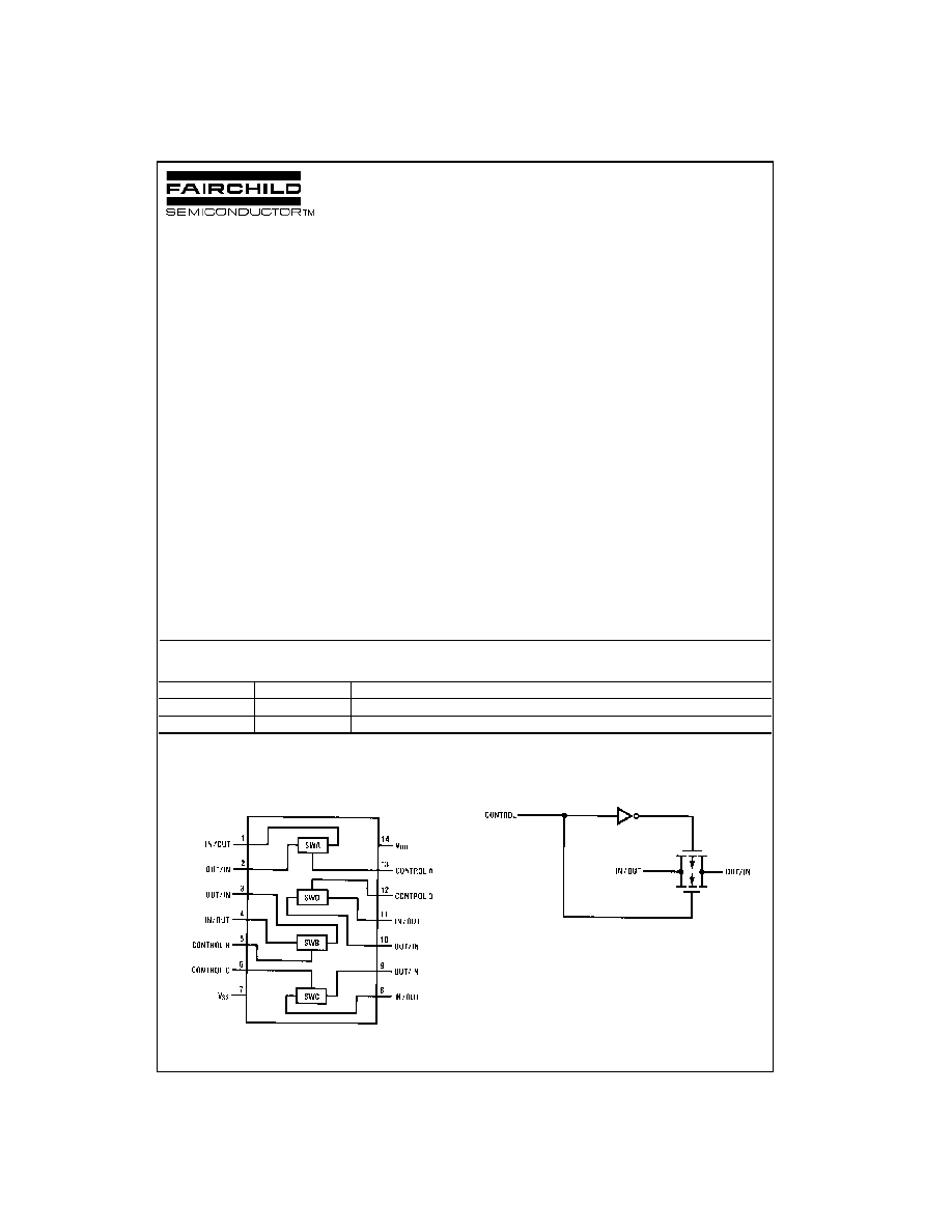
Connection Diagram
Pin Assignments for DIP and SOIC
Schematic Diagram
Order Number
Package Number
Package Description
CD4016BCM
M14A
14-Lead Small Outline Integrated Circuit (SOIC), JEDEC MS-120, 0.150" Narrow
CD4016BCN
N14A
14-Lead Plastic Dual-In-Line Package (PDIP), JEDEC MS-001, 0.300" Wide
www.fairchildsemi.com
2
C
D
40
16BC
Absolute Maximum Ratings
(Note 1)
(Note 2)
Recommended Operating
Conditions
(Note 2)
Note 1: "Absolute Maximum Ratings" are those values beyond which the
safety of the device cannot be guaranteed. They are not meant to imply
that the devices should be operated at these limits. The tables of "Recom-
mended Operating Conditions" and "Electrical Characteristics" provide con-
ditions for actual device operation.
Note 2: V
SS
=
0V unless otherwise specified.
DC Electrical Characteristics
(Note 2)
Note 3: If the switch input is held at V
DD
, V
IHC
is the control input level that will cause the switch output to meet the standard "B" series V
OH
and I
OH
output
levels. If the analog switch input is connected to V
SS
, V
IHC
is the control input level -- which allows the switch to sink standard "B" series |I
OH
|, high level cur-
rent, and still maintain a V
OL
"B" series. These currents are shown in Figure 8.
V
DD
Supply Voltage
-
0.5V to
+
18V
V
IN
Input Voltage
-
0.5V to V
DD
+
0.5V
T
S
Storage Temperature Range
-
65
∞
C to
+
150
∞
C
Power Dissipation (P
D
)
Dual-In-Line
700 mW
Small Outline
500 mW
Lead Temperature
(Soldering, 10 seconds)
260
∞
C
V
DD
Supply Voltage
3V to 15V
V
IN
Input Voltage
0V to V
DD
T
A
Operating Temperature Range
-
40
∞
C to
+
85
∞
C
Symbol
Parameter
Conditions
-
40
∞
C
25
∞
C
+
85
∞
C
Units
Min
Max
Min
Typ
Max
Min
Max
I
DD
Quiescent Device
V
DD
=
5V, V
IN
=
V
DD
or V
SS
1.0
0.01
1.0
7.5
µ
A
Current
V
DD
=
10V, V
IN
=
V
DD
or V
SS
2.0
0.01
2.0
15
µ
A
V
DD
=
15V, V
IN
=
V
DD
or V
SS
4.0
0.01
4.0
30
µ
A
Signal Inputs and Outputs
R
ON
"ON" Resistance
R
L
=
10k
to (V
DD
-
V
SS
)/2
V
C
=
V
DD
, V
IS
=
V
SS
or V
DD
V
DD
=
10V
610
275
660
840
V
DD
=
15V
370
200
400
520
R
L
=
10k
to (V
DD
-
V
SS
)/2
V
C
=
V
DD
V
DD
=
10V, V
IS
=
4.75 to 5.25V
1900
850
2000
2380
V
DD
=
15V, V
IS
=
7.25 to 7.75V
790
400
850
1080
R
ON
"ON" Resistance
R
L
=
10k
to (V
DD
-
V
SS
)/2
Between any 2 of
V
C
=
V
DD
, V
IS
=
V
SS
to V
DD
4 Switches
V
DD
=
10V
15
(In Same Package)
V
DD
=
15V
10
I
IS
Input or Output
V
C
=
0, V
DD
=
15V
±
50
±
0.1
±
50
±
200
nA
Leakage
V
IS
=
0V or 15V,
Switch "OFF"
V
OS
=
15V or 0V
Control Inputs
V
ILC
LOW Level Input
V
IS
=
V
SS
and V
DD
Voltage
V
OS
=
V
DD
and V
SS
I
IS
=
±
10
µ
A
V
DD
=
5V
0.9
0.7
0.4
V
V
DD
=
10V
0.9
0.7
0.4
V
V
DD
=
15V
0.9
0.7
0.4
V
V
IHC
HIGH Level Input
V
DD
=
5V
3.5
3.5
3.5
V
Voltage
V
DD
=
10V
7.0
7.0
7.0
V
V
DD
=
15V
11.0
11.0
11.0
V
(Note 3) and Figure 8
I
IN
Input Current
V
CC
-
V
SS
=
15V
±
0.3
±
10
-
5
±
0.3
±
1.0
µ
A
V
DD
V
IS
V
SS
V
DD
V
C
V
SS
3
www.fairchildsemi.com
CD401
6BC
AC Electrical Characteristics
(Note 4)
T
A
=
25
∞
C, t
r
=
t
f
=
20 ns and V
SS
=
0V unless otherwise specified
Note 4: AC Parameters are guaranteed by DC correlated testing.
Note 5: These devices should not be connected to circuits with the power "ON".
Note 6: In all cases, there is approximately 5 pF of probe and jig capacitance on the output; however, this capacitance is included in C
L
wherever it is speci-
fied.
Note 7: V
IS
is the voltage at the in/out pin and V
OS
is the voltage at the out/in pin. V
C
is the voltage at the control input.
Symbol
Parameter
Conditions
Min
Typ
Max
Units
t
PHL
, t
PLH
Propagation Delay Time
V
C
=
V
DD
, C
L
=
50 pF, (Figure 1)
Signal Input to Signal Output
R
L
=
200k
V
DD
=
5V
58
100
ns
V
DD
=
10V
27
50
ns
V
DD
=
15V
20
40
ns
t
PZH
, t
PZL
Propagation Delay Time
R
L
=
1.0 k
, C
L
=
50 pF, (Figure 2, Figure 3)
Control Input to Signal
V
DD
=
5V
20
50
ns
Output HIGH Impedance to
V
DD
=
10V
18
40
ns
Logical Level
V
DD
=
15V
17
35
ns
t
PHZ
, t
PLZ
Propagation Delay Time
R
L
=
1.0 k
, C
L
=
50 pF, (Figure 2, Figure 3)
Control Input to Signal
V
DD
=
5V
15
40
ns
Output Logical Level to
V
DD
=
10V
11
25
ns
HIGH Impedance
V
DD
=
15V
10
22
ns
Sine Wave Distortion
V
C
=
V
DD
=
5V, V
SS
=
-
5
0.4
%
R
L
=
10 k
, V
IS
=
5 V
P-P
, f
=
1 kHz,
(Figure 4)
Frequency Response -- Switch
V
C
=
V
DD
=
5V, V
SS
=
-
5V,
40
MHz
"ON" (Frequency at
-
3 dB)
R
L
=
1 k
, V
IS
=
5 V
P-P
,
20 Log
10
V
OS
/V
OS
(1 kHz)
-
dB,
(Figure 4)
Feedthrough -- Switch "OFF"
V
DD
=
5V, V
C
=
V
SS
=
-
5V,
1.25
MHz
(Frequency at
-
50 dB)
R
L
=
1 k
, V
IS
=
5 V
P-P
,
20 Log
10
(V
OS
/V
IS
)
=
-
50 dB,
(Figure 4)
Crosstalk Between Any Two
V
DD
=
V
C(A)
=
5V; V
SS
=
V
C(B)
=
-
5V,
0.9
MHz
Switches (Frequency at
-
50 dB)
R
L
=
1 k
V
IS(A)
=
5 V
P-P
,
20 Log
10
(V
OS(B)
/V
OS(A)
)
=
-
50 dB,
(Figure 5)
Crosstalk; Control Input to
V
DD
=
10V, R
L
=
10 k
150
mV
P-P
Signal Output
R
IN
=
1 k
, V
CC
=
10V Square Wave,
C
L
=
50 pF (Figure 6)
Maximum Control Input
R
L
=
1 k
, C
L
=
50 pF, (Figure 7)
V
OS(f)
=
Ω V
OS
(1 kHz)
V
DD
=
5V
6.5
MHz
V
DD
=
10V
8.0
MHz
V
DD
=
15V
9.0
MHz
C
IS
Signal Input Capacitance
4
pF
C
OS
Signal Output Capacitance
V
DD
=
10V
4
pF
C
IOS
Feedthrough Capacitance
V
C
=
0V
0.2
pF
C
IN
Control Input Capacitance
5
7.5
pF
www.fairchildsemi.com
4
C
D
40
16BC
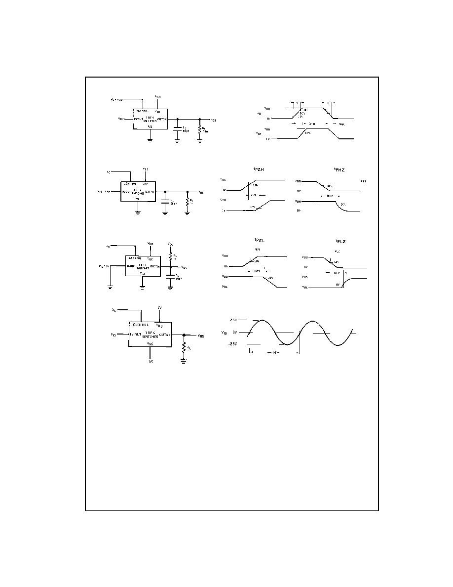
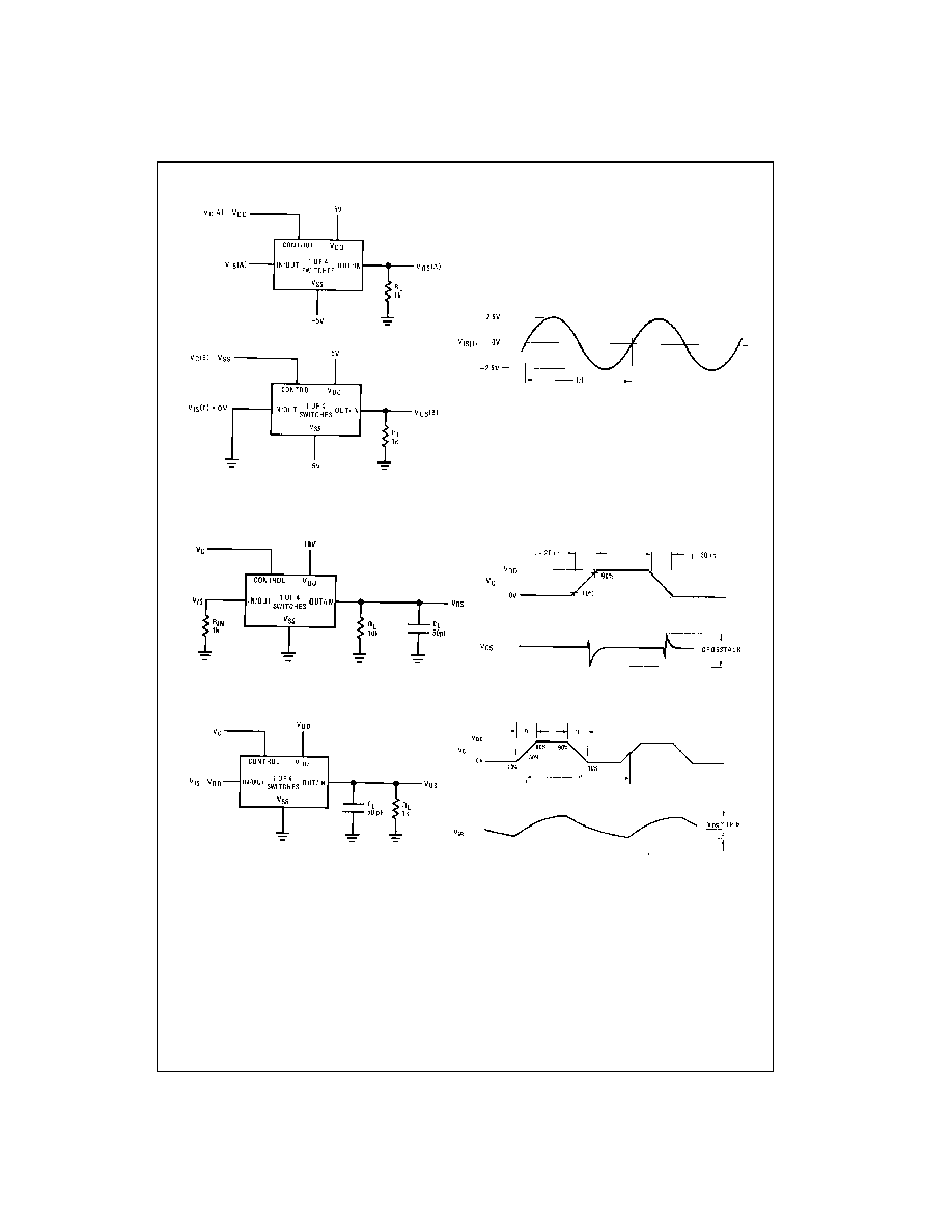
AC Test Circuits and Switching Time Waveforms
FIGURE 1. t
PLH
, t
PLH
Propagation Delay Time Control to Signal Output
FIGURE 2. t
PZH
, t
PHZ
Propagation Delay Time Control to Signal Output
FIGURE 3. t
PZH
, t
PHZ
Propagation Delay Time Control to Signal Output
V
C
=
V
DD
for distortion and frequency response tests
V
C
=
V
SS
for feedthrough test
FIGURE 4. Sine Wave Distortion, Frequency Response and Feedthrough
5
www.fairchildsemi.com
CD401
6BC
AC Test Circuits and Switching Time Waveforms
(Continued)
FIGURE 5. Crosstalk Between Any Two Switches
FIGURE 6. Crosstalk -- Control to Input Signal Output
FIGURE 7. Maximum Control Input Frequency