© 2000 Fairchild Semiconductor Corporation
DS008773
www.fairchildsemi.com
March 1986
Revised February 2000
DM74ALS14 Hex Inver
ter
wi
th Schm
i
t
t
T
r
ig
ger Input
s
DM74ALS14
Hex Inverter with Schmitt Trigger Inputs
General Description
This device contains six independent gates, each of which
performs the logic INVERT function. Each input has hyster-
esis which increases the noise immunity and transforms a
slowly changing input signal to a fast changing, jitter-free
output.
Features
s
Input hysteresis
s
Low output noise generation
s
High input noise immunity
s
Switching specification at 50 pF
s
Switching specifications guaranteed over full tempera-
ture and V
CC
range
s
Advanced oxide-isolated, ion-implanted Schottky TTL
process
s
Functionally and pin-for-pin compatible with Schottky
and low power Schottky TTL counterparts
s
Improved AC performance over low power Schottky
counterpart
Ordering Code:
Devices also available in Tape and Reel. Specify by appending the suffix letter "X" to the ordering code.
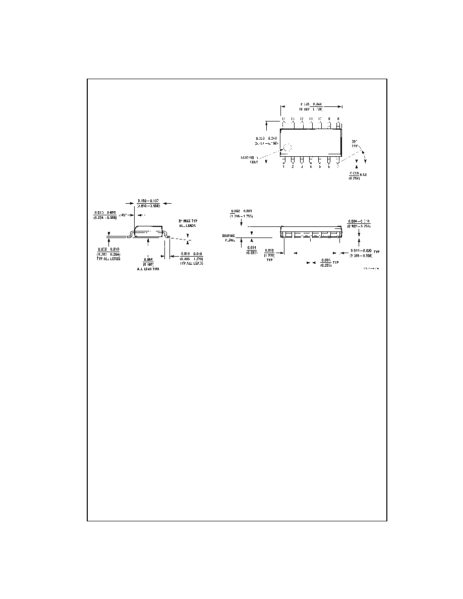
Connection Diagram
Function Table
Y
=
A
H
=
HIGH Logic Level
L
=
LOW Logic Level
Order Number
Package Number
Package Description
DM74ALS14M
M14A
14-Lead Small Outline Integrated Circuit (SOIC), JEDEC MS-012, 0.150 Narrow
DM74ALS14SJ
M14D
14-Lead Small Outline Package (SOP), EIAJ TYPE II, 5.3mm Wide
DM74ALS14N
N14A
14-Lead Plastic Dual-In-Line Package (PDIP), JEDEC MS-001, 0.300 Wide
Input
Output
A
Y
L
H
H
L

www.fairchildsemi.com
2
DM
74ALS14
Absolute Maximum Ratings
(Note 1)
Note 1: The "Absolute Maximum Ratings" are those values beyond which
the safety of the device cannot be guaranteed. The device should not be
operated at these limits. The parametric values defined in the Electrical
Characteristics tables are not guaranteed at the absolute maximum ratings.
The "Recommended Operating Conditions" table will define the conditions
for actual device operation.
Recommended Operating Conditions
Electrical Characteristics
over recommended free air temperature range (unless otherwise noted)
Note 2: Plastic DIP package.
Note 3: n
=
number of device outputs, n
-
1 outputs switching, each driven 0V to 3V one output @ GND.
Note 4: n
=
number of device outputs, n outputs switching, n
-
1 inputs switching 0V to 3V. Input under test switching 3V to threshold (V
ILD
); 0V to threshold
(V
IHD
); f
=
1 MHz.
Supply Voltage
7V
Input Voltage
7V
Storage Temperature Range
-
65
∞
C to
+
150
∞
C
Operating Free Air Temperature Range
0
∞
C to
+
70
∞
C
Typical
JA
N Package
78.5
∞
C/W
M Package
109.0
∞
C/W
Symbol
Parameter
Min
Nom
Max
Units
V
CC
Supply Voltage
4.5
5
5.5
V
V
T
+
Positive-Going Input
V
CC
=
Min to Max
1.4
2
V
Threshold Voltage
V
CC
=
5V
1.55
1.85
V
T
-
Negative-Going Input
V
CC
=
Min to Max
0.75
1.2
V
Threshold Voltage
V
CC
=
5V
0.85
1.1
HYS
Input Hysteresis
V
CC
=
Min to Max
0.5
V
V
CC
=
5V
0.6
I
OH
HIGH Level Output Current
-
0.4
mA
I
OL
LOW Level Output Current
8
mA
T
A
Operating Free Air Temperature Range
0
70
∞
C
Symbol
Parameter
Test Conditions
Min
Typ
Max
Units
V
IK
Input Clamp Voltage
V
CC
=
Min, I
I
=
-
18 mA
-
1.5
V
V
OH
HIGH Level Output Voltage
V
CC
=
4.5V to 5.5V, I
OH
=
Max
V
CC
-
2
V
V
OL
LOW Level Output Voltage
V
CC
=
Min
I
OL
=
4 mA
0.25
0.4
V
I
OL
=
8 mA
0.35
0.5
V
I
T
+
Input Current at Positive-Going Threshold Voltage
V
CC
=
5V, V
I
=
V
T
+
20
µ
A
I
T
-
Input Current at Negative-Going Threshold Voltage V
CC
=
5V, V
I
=
V
T
-
-
100
µ
A
I
I
Input Current at Maximum Input Voltage
V
CC
=
Max, V
I
=
7V
100
µ
A
I
IH
HIGH Level Input Current
V
CC
=
Max, V
I
=
2.7V
20
µ
A
I
IL
LOW Level Input Current
V
CC
=
Max, V
I
=
0.4V
-
100
µ
A
I
O
Output Drive Current
V
CC
=
Max, V
O
=
2.25V
-
30
-
112
mA
I
CCH
Supply Current with Outputs HIGH
V
CC
=
Max
12
mA
I
CCL
Supply Current with Outputs LOW
V
CC
=
Max
12
mA
V
OLP
Quiet Output Maximum
V
CC
=
5.0V, T
A
=
25
∞
C
0.16
V
Dynamic V
OL
(Figures 1, 2); (Note 2)(Note 3)
V
OLV
Quiet Output Minimum
V
CC
=
5.0V, T
A
=
25
∞
C
-
0.27
V
Dynamic V
OL
(Figures 1, 2); (Note 2)(Note 3)
V
IHD
Minimum HIGH Level
V
CC
=
5.0V, T
A
=
25
∞
C
1.44
V
Dynamic Input Voltage
(Note 2)(Note 4)
V
ILD
Maximum LOW Level
V
CC
=
5.0V, T
A
=
25
∞
C
1.15
V
Dynamic Input Voltage
(Note 2)(Note 4)
3
www.fairchildsemi.com
DM74ALS14
Switching Characteristics
over recommended operating free air temperature range
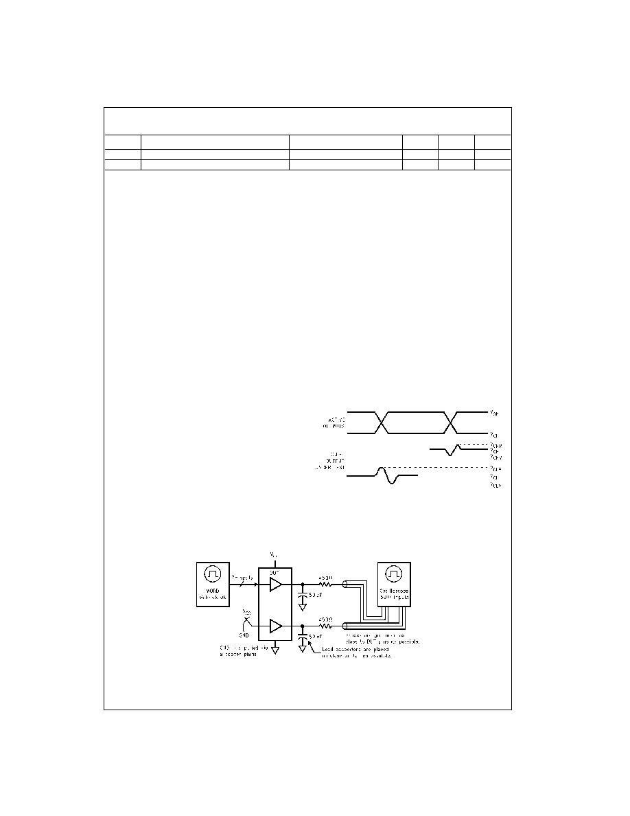
ALS Noise Characteristics
The setup of a noise characteristics measurement is critical
to the accuracy and repeatability of the tests. The following
is a brief description of the setup used to measure the
noise characteristics of ALS.
Equipment:
Word Generator
Printed Circuit Board Test Fixture
Dual Trace Oscillo-
scope
Procedure:
1. Verify Test Fixture Loading: Standard Load 50 pF,
500
.
2. Deskew the word generator so that no two channels
have greater than 150 ps skew between them. This
requires that the oscilloscope be deskewed first. Swap
out the channels that have more than 150 ps of skew
until all channels being used are within 150 ps. It is
important to deskew the word generator channels
before testing. This will ensure that the outputs switch
simultaneously.
3. Terminate all inputs and outputs to ensure proper load-
ing of the outputs and that the input levels are at the
correct voltage.
4. Set V
CC
to 5.0V.
5. Set the word generator to toggle all but one output at a
frequency of 1 MHz. Greater frequencies will increase
DUT heating and affect the results of the measure-
ment.
6. Set the word generator input levels at 0V LOW and 3V
HIGH. Verify levels with a digital volt meter.
V
OLP
/V
OLV
and V
OHP
/V
OHV
:
∑ Determine the quiet output pin that demonstrates the
greatest noise levels. The worst case pin will usually be
the furthest from the ground pin. Monitor the output volt-
ages using a 50
coaxial cable plugged into a standard
SMB type connector on the test fixture. Do not use an
active FET probe.
∑ Verify that the GND reference recorded on the oscillo-
scope has not drifted to ensure the accuracy and repeat-
ability of the measurements.
V
ILD
and V
IHD
:
∑ Monitor one of the switching outputs using a 50
coaxial
cable plugged into a standard SMB type connector on
the test fixture. Do not use an active FET probe.
∑ First increase the input LOW voltage level, V
IL
, until the
output begins to oscillate. Oscillation is defined as noise
on the output LOW level that exceeds V
IL
limits, or on
output HIGH levels that exceed V
IH
limits. The input
LOW voltage level at which oscillation occurs is defined
as V
ILD
.
∑ Next decrease the input HIGH voltage level on the word
generator, V
IH
until the output begins to oscillate. Oscil-
lation is defined as noise on the output LOW level that
exceeds V
IL
limits, or on output HIGH levels that exceed
V
IH
limits. The input HIGH voltage level at which oscilla-
tion occurs is defined as V
IHD
.
∑ Verify that the GND reference recorded on the oscillo-
scope has not drifted to ensure the accuracy and repeat-
ability of the measurements.
V
OHV
and V
OHP
are measured with respect to V
OH
reference. V
OLV
and
V
OLP
are measured with respect to ground reference.
Input pulses have the following characteristics: f
=
1 MHz, t
r
=
3 ns, t
f
=
3 ns, skew
<
150 ps.
FIGURE 1. Quiet Output Noise Voltage Waveforms
FIGURE 2. Simultaneous Switching Test Circuit
Symbol
Parameter
Conditions Min
Max
Units
t
PLH
Propagation Delay Time LOW-to-HIGH Level Output
V
CC
=
4.5V to 5.5V
2
12
ns
t
PHL
Propagation Delay Time HIGH-to-LOW Level Output
R
L
=
500
, C
L
=
50 pF
2
10
ns