© 2000 Fairchild Semiconductor Corporation
DS006400
www.fairchildsemi.com
August 1986
Revised March 2000
DM74LS166
8-
Bit
Par
a
ll
el-
I
n
/
Ser
i
al
-Out
Shi
f
t
Regi
ster
DM74LS166
8-Bit Parallel-In/Serial-Out Shift Register
General Description
These parallel-in or serial-in, serial-out shift registers fea-
ture gated clock inputs and an overriding clear input. All
inputs are buffered to lower the drive requirements to one
normalized load, and input clamping diodes minimize
switching transients to simplify system design. The load
mode is established by the shift/load input. When HIGH,
this input enables the serial data input and couples the
eight flip-flops for serial shifting with each clock pulse.
When LOW, the parallel (broadside) data inputs are
enabled and synchronous loading occurs on the next clock
pulse. During parallel loading, serial data flow is inhibited.
Clocking is accomplished on the LOW-to-HIGH level edge
of the clock pulse through a two-input NOR gate, permitting
one input to be used as a clock-enable or clock-inhibit func-
tion. Holding either of the clock inputs HIGH inhibits clock-
ing; holding either LOW enables the other clock input. This
allows the system clock to be free running, and the register
can be stopped on command with the other clock input.
The clock-inhibit input should be changed to the high level
only while the clock input is HIGH. A buffered, direct clear
input overrides all other inputs, including the clock, and
sets all flip-flops to zero.
Ordering Code:
Devices also available in Tape and Reel. Specify by appending the suffix letter "X" to the ordering code.
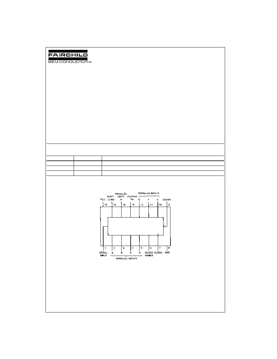
Connection Diagram
Order Number
Package Number
Package Description
DM74LS166M
M16A
16-Lead Small Outline Integrated Circuit (SOIC), JEDEC MS-012, 0.150 Narrow
DM74LS166WM
M16B
16-Lead Small Outline Intergrated Circuit (SOIC), JEDEC MS-013, 0.300 Wide
DM74LS166N
N16E
16-Lead Plastic Dual-In-Line Package (PDIP), JEDEC MS-001, 0.300 Wide

www.fairchildsemi.com
2
DM74LS166
Function Table
H
=
HIGH Level (steady state)
L
=
LOW Level (steady state)
X
=
Don't Care (any input, including transitions)
=
Transition from LOW-to-HIGH level
a...h
=
The level of steady-state input at inputs A through H, respectively
Q
A0
, Q
B0
, Q
H0
=
The level of Q
A
, Q
B
, Q
H
, respectively, before the indicated steady-state input conditions were established
Q
An
, Q
Gn
,
=
The level of Q
A
, Q
G
, respectively, before the most recent
transition of the clock
Logic Diagram
Timing Diagram
Typical Clear, Shift, Load, Inhibit and Shift Sequences
Inputs
Internal
Output
Clear
Shift/
Clock
Clock
Serial
Parallel
Outputs
Q
H
Load
Inhibit
A...H
Q
A
Q
B
L
X
X
X
X
X
L
L
L
H
X
L
L
X
X
Q
A0
Q
B0
Q
H0
H
L
L
X
a...h
a
b
h
H
H
L
H
X
H
Q
An
Q
Gn
H
H
L
L
X
L
Q
An
Q
Gn
H
X
H
X
X
Q
A0
Q
B0
Q
H0

3
www.fairchildsemi.com
DM74LS166
Absolute Maximum Ratings
(Note 1)
Note 1: The "Absolute Maximum Ratings" are those values beyond which
the safety of the device cannot be guaranteed. The device should not be
operated at these limits. The parametric values defined in the Electrical
Characteristics tables are not guaranteed at the absolute maximum ratings.
The "Recommended Operating Conditions" table will define the conditions
for actual device operation.
Recommended Operating Conditions
Note 2: C
L
=
15 pF, R
L
=
2 k
, T
A
=
25
∞
C and V
CC
=
5V.
Note 3: C
L
=
50 pF, R
L
=
2 k
, T
A
=
25
∞
C and V
CC
=
5V.
Note 4: T
A
=
25
∞
C and V
CC
=
5V.
Electrical Characteristics
over recommended operating free air temperature range (unless otherwise noted)
Note 5: All typicals are at V
CC
=
5V, T
A
=
25
∞
C.
Note 6: Not more than one output should be shorted at a time, and the duration should not exceed one second.
Note 7: With all outputs OPEN, 4.5V applied to the serial input, all other inputs except the CLOCK grounded, I
CC
is measured after a momentary ground,
then 4.5V is applied to the CLOCK.
Supply Voltage
7V
Input Voltage
7V
Operating Free Air Temperature Range
0
∞
C to
+
70
∞
C
Storage Temperature Range
-
65
∞
C to
+
150
∞
C
Symbol
Parameter
Min
Nom
Max
Units
V
CC
Supply Voltage
4.75
5
5.25
V
V
IH
HIGH Level Input Voltage
2
V
V
IL
LOW Level Input Voltage
0.8
V
I
OH
HIGH Level Output Current
-
0.4
mA
I
OL
LOW Level Output Current
8
mA
f
CLK
Clock Frequency (Note 2)
0
25
MHz
Clock Frequency (Note 3)
0
20
MHz
t
W
Pulse Width (Note 4)
Clock
20
ns
Clear
20
t
SU
Setup Time (Note 4)
Mode
30
ns
Data
20
t
H
Hold Time (Note 4)
0
ns
T
A
Free Air Operating Temperature
0
70
∞
C
Symbol
Parameter
Conditions
Min
Typ
Max
Units
(Note 5)
V
I
Input Clamp Voltage
V
CC
=
Min, I
I
=
-
18 mA
-
1.5
V
V
OH
HIGH Level
V
CC
=
Min, I
OH
=
Max
2.7
3.4
V
Output Voltage
V
IL
=
Max, V
IH
=
Min
V
OL
LOW
Level V
CC
=
Min, I
OL
=
Max
0.35
0.5
Output Voltage
V
IL
=
Max, V
IH
=
Min
V
I
OL
=
4 mA, V
CC
=
Min
0.25
0.4
I
I
Input Current @ Max Input Voltage
V
CC
=
Max, V
I
=
7V
0.1
mA
I
IH
HIGH Level Input Current
V
CC
=
Max, V
I
=
2.7V
20
µ
A
I
IL
LOW Level Input Current
V
CC
=
Max, V
I
=
0.4V
-
0.4
mA
I
OS
Short Circuit Output Current
V
CC
=
Max (Note 6)
-
20
-
100
mA
I
CC
Supply Current
V
CC
=
Max (Note 7)
22
38
mA

www.fairchildsemi.com
4
DM74LS166
Switching Characteristics
at V
CC
=
5V and T
A
=
25
∞
C
Parameter Measurement Information
Voltage Waveforms
Test Table for Synchronous Inputs
Note A: The clock pulse has the following characteristics: t
W(clock)
20 ns and PRR
=
1 MHz. The clear pulse has the following characteristics:
t
W(clear)
20 ns and t
HOLD
=
0 ns. When testing f
MAX
, vary the clock PRR.
Note B: A clear pulse is applied prior to each test.
Note C: Propagation delay times (t
PLH
and t
PHL
) are measured at t
n
+
1
. Proper shifting of data is verified at t
n
+
8
with a functional test.
Note D: t
n
=
bit time before clocking transition
t
n
+
1
=
bit time after one clocking transition
t
n
+
8
=
bit time after eight clocking transitions
Note E: V
REF
=
1.3V.
From (Input)
R
L
=
2 k
Symbol
Parameter
To (Output)
C
L
=
15 pF
C
L
=
50 pF
Units
Min
Max
Min
Max
f
MAX
Maximum Clock Frequency
25
20
MHz
t
PLH
Propagation Delay Time
Clock to Output
8
35
38
ns
LOW-to-HIGH Level Output
t
PHL
Propagation Delay Time
Clock to Output
8
35
41
ns
HIGH-to-LOW Level Output
t
PHL
Propagation Delay Time
Clear to Output
6
30
36
ns
HIGH-to-LOW Level Output
Data Input
Shift/Load
Output Tested
for Test
(See Note C)
H
0V
Q
H
at T
N
+
1
Serial Input
4.5V
Q
H
at T
N
+
8

5
www.fairchildsemi.com
DM74LS166
Physical Dimensions
inches (millimeters) unless otherwise noted
16-Lead Small Outline Integrated Circuit (SOIC), JEDEC MS-012, 0.150 Narrow
Package Number M16A
16-Lead Small Outline Intergrated Circuit (SOIC), JEDEC MS-013, 0.300 Wide
Package Number M16B