Äîêóìåíòàöèÿ è îïèñàíèÿ www.docs.chipfind.ru
© 1999 Fairchild Semiconductor Corporation
DS006417
www.fairchildsemi.com
June 1989
Revised November 1999
DM74LS257
B
3-
ST
A
T
E Q
u
ad
2-
Data Sele
ctor
s/Mul
t
i
p
lexer
s
DM74LS257B
3-STATE Quad 2-Data Selectors/Multiplexers
General Description
These Schottky-clamped high-performance multiplexers
feature 3-STATE outputs that can interface directly with
data lines of bus-organized systems. With all but one of the
common outputs disabled (at a high impedance state), the
low impedance of the single enabled output will drive the
bus line to a HIGH or LOW logic level. To minimize the pos-
sibility that two outputs will attempt to take a common bus
to opposite logic levels, the output enable circuitry is
designed such that the output disable times are shorter
than the output enable times.
This 3-STATE output feature means that n-bit (paralleled)
data selectors with up to 258 sources can be implemented
for data buses. It also permits the use of standard TTL reg-
isters for data retention throughout the system.
Features
s
3-STATE versions LS157 and LS158 with same pinouts
s
Schottky-clamped for significant improvement in A-C
performance
s
Provides bus interface from multiple sources in
high-performance systems
s
Average propagation delay from data input 12 ns
s
Typical power dissipation:
50 mW
Ordering Code:
Devices also available in Tape and Reel. Specify by appending the suffix letter "X" to the ordering code.
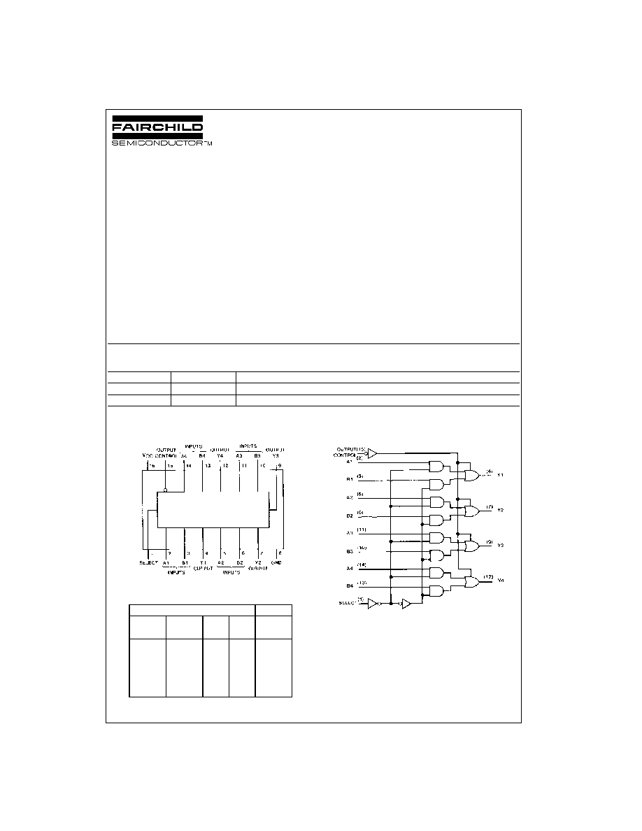
Connection Diagram
Function Table
H
=
HIGH Level
X
=
Don't Care
L
=
LOW Level
Z
=
High Impedance (off)
Logic Diagram
Order Number
Package Number
Package Description
DM74LS257BM
M16A
16-Lead Small Outline Integrated Circuit (SOIC), JEDEC MS-012, 0.150 Narrow
DM74LS257BN
N16E
16-Lead Plastic Dual-In-Line Package (PDIP), JEDEC MS-001, 0.300 Wide
Inputs
Output Y
Output
Select
A
B
LS257
Control
H
X
X
X
Z
L
L
L
X
L
L
L
H
X
H
L
H
X
L
L
L
H
X
H
H
www.fairchildsemi.com
2
D
M
74LS25
7B
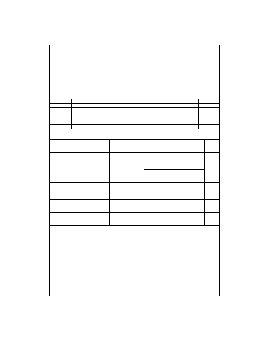
Absolute Maximum Ratings
(Note 1)
Note 1: The "Absolute Maximum Ratings" are those values beyond which
the safety of the device cannot be guaranteed. the device should not be
operated at these limits. The parametric values defined in the Electrical
Characteristics tables are not guaranteed at the absolute maximum ratings.
The Recommended Operating Conditions table will define the conditions
for actual device operation.
Recommended Operating Conditions
DC Electrical Characteristics
Note 2: All typicals are at V
CC
=
5V, T
A
=
25
°
C.
Note 3: Not more than one output should be shorted at a time, and the duration should not exceed one second.
Note 4: I
CC
is measured with all outputs open and all possible inputs grounded, while achieving the stated output conditions.
Supply Voltage
7V
Input Voltage
7V
Operating Free Air Temperature Range
0
°
C to
+
70
°
C
Storage Temperature Range
-
65
°
C to
+
150
°
C
Symbol
Parameter
Min
Nom
Max
Units
V
CC
Supply Voltage
4.75
5
5.25
V
V
IH
HIGH Level Input Voltage
2
V
V
IL
LOW Level Input Voltage
0.8
V
I
OH
HIGH Level Output Current
-
2.6
mA
I
OL
LOW Level Output Current
24
mA
T
A
Free Air Operating Temperature
0
70
°
C
Symbol
Parameter
Conditions
Min
Typ
Max
Units
(Note 2)
V
I
Input Clamp Voltage
V
CC
=
Min, I
I
=
-
18 mA
-
1.5
V
V
OH
HIGH Level Output Voltage
V
IL
=
Max, V
IH
=
Min
2.4
3.1
V
V
OL
LOW Level Output
V
IL
=
Max, V
IH
=
Min
0.35
0.5
V
Voltage
I
OL
=
12 mA, V
CC
=
Min
0.25
0.4
I
I
Input Current @ Max
V
CC
=
Max,
Select
0.2
mA
Input Voltage
V
I
=
7V
Other
0.1
I
IH
HIGH Level Input
V
CC
=
Max,
Select
40
µ
A
Current
V
I
=
2.7V
Other
20
I
IL
LOW Level Input
V
CC
=
Max,
Select
-
0.8
mA
Current
V
I
=
0.4V
Other
-
0.4
I
OZH
OFF-State Output Current with
V
CC
=
Max, V
O
=
2.7V
20
µ
A
HIGH Level Output Voltage Applied
V
IH
=
Min, V
IL
=
Max
I
OZL
OFF-State Output Current with
V
CC
=
Max, V
O
=
0.4V
-
20
µ
A
LOW Level Output Voltage Applied
V
IH
=
Min, V
IL
=
Max
I
OS
Short Circuit Output Current
V
CC
=
Max (Note 3)
-
20
-
100
mA
I
CCH
Supply Current with Outputs HIGH
V
CC
=
Max (Note 4)
5.9
10
mA
I
CCL
Supply Current with Outputs LOW
V
CC
=
Max (Note 4)
9.2
16
mA
I
CCZ
Supply Current with Outputs Disabled V
CC
=
Max (Note 4)
12
19
mA
3
www.fairchildsemi.com
DM74LS257
B
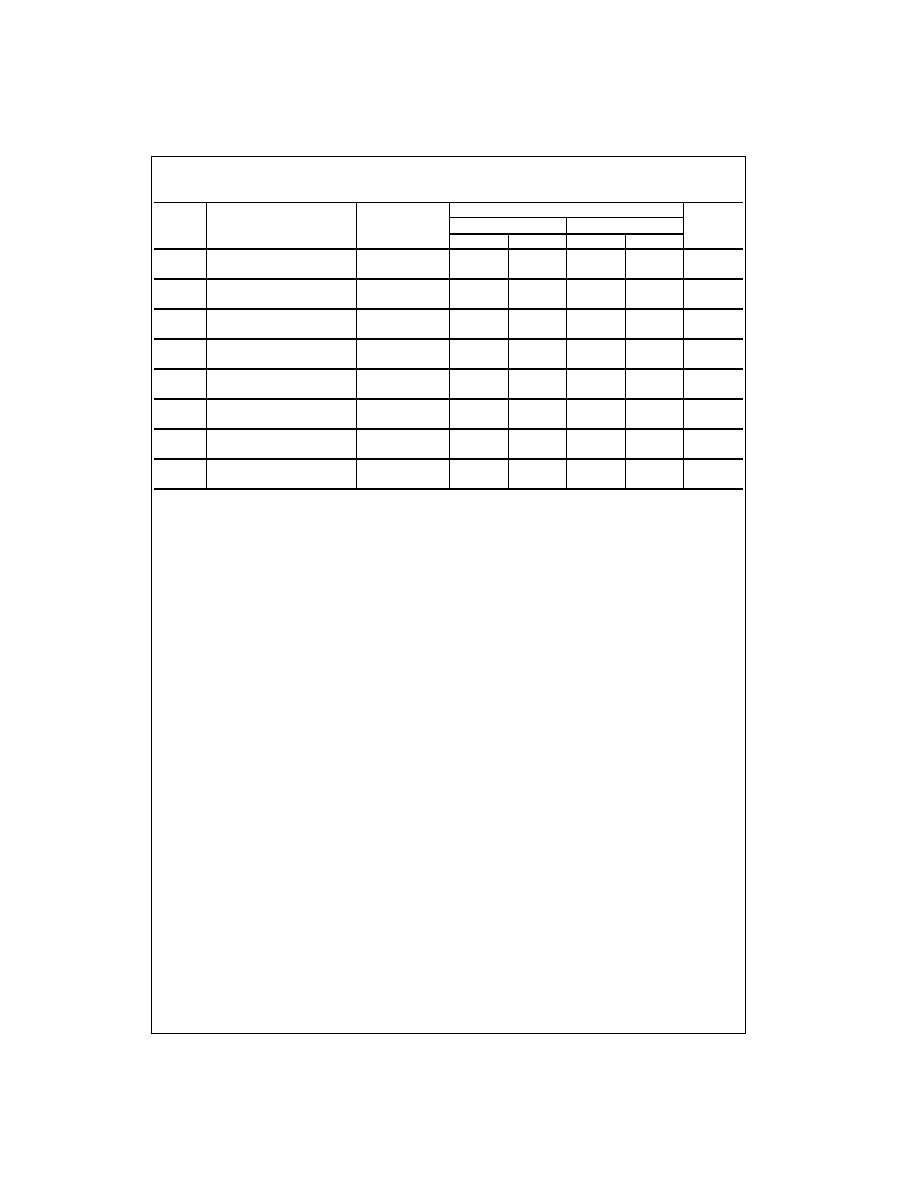
Switching Characteristics
V
CC
=
5V and T
A
=
25
°
C
Note 5: C
L
=
5 pF
Symbol
Parameter
RL
=
667
Units
From (Input)
C
L
=
45 pF
C
L
=
150 pF
To (Output)
Min
Max
Min
Max
t
PLH
Propagation Delay Time
Data to Output
18
27
ns
LOW-to-HIGH Level Output
t
PHL
Propagation Delay Time
Data to Output
18
27
ns
HIGH-to-LOW Level Output
t
PLH
Propagation Delay Time
Select to Output
28
35
ns
LOW-to-HIGH Level Output
t
PHL
Propagation Delay Time
Select to Output
35
42
ns
HIGH-to-LOW Level Output
t
PZH
Output Enable Time
Output Control to Y
15
27
ns
to HIGH Level Output
t
PZL
Output Enable Time
Output Control to Y
28
38
ns
to LOW Level Output
t
PHZ
Output Disable Time from
Output Control to Y
28
ns
HIGH Level Output (Note 5)
t
PLZ
Output Disable Time from
Output Control to Y
25
ns
LOW Level Output (Note 5)
www.fairchildsemi.com
4
D
M
74LS25
7B
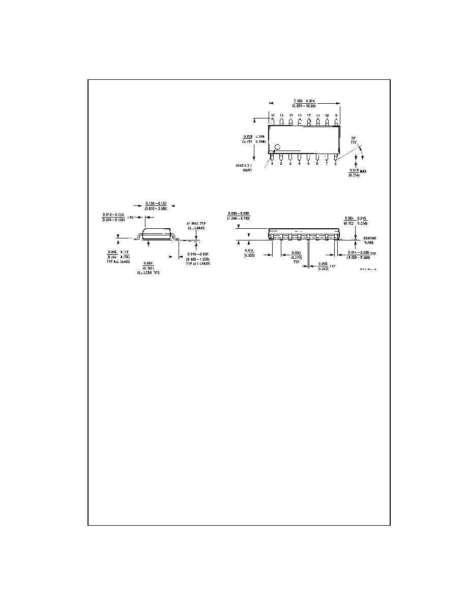
Physical Dimensions
inches (millimeters) unless otherwise noted
16-Lead Small Outline Integrated Circuit (SOIC), JEDEC MS-012, 0.150 Narrow
Package Number M16A
Physical Dimensions
inches (millimeters) unless otherwise noted (Continued)
5
www.fairchildsemi.com
DM74LS257
B
3-
ST
A
T
E Q
u
ad
2-
Data Sele
ctor
s/Mul
t
i
p
lexer
s
Physical Dimensions
inches (millimeters) unless otherwise noted (Continued)
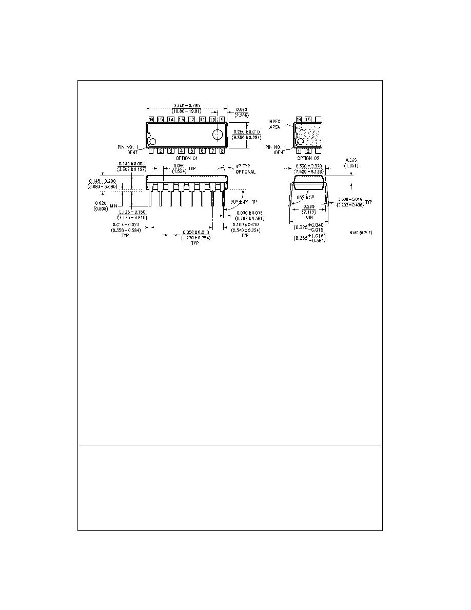
16-Lead Plastic Dual-In-Line Package (PDIP), JEDEC MS-001, 0.300 Wide
Package Number N16E
Fairchild does not assume any responsibility for use of any circuitry described, no circuit patent licenses are implied and
Fairchild reserves the right at any time without notice to change said circuitry and specifications.
LIFE SUPPORT POLICY
FAIRCHILD'S PRODUCTS ARE NOT AUTHORIZED FOR USE AS CRITICAL COMPONENTS IN LIFE SUPPORT
DEVICES OR SYSTEMS WITHOUT THE EXPRESS WRITTEN APPROVAL OF THE PRESIDENT OF FAIRCHILD
SEMICONDUCTOR CORPORATION. As used herein:
1. Life support devices or systems are devices or systems
which, (a) are intended for surgical implant into the
body, or (b) support or sustain life, and (c) whose failure
to perform when properly used in accordance with
instructions for use provided in the labeling, can be rea-
sonably expected to result in a significant injury to the
user.
2. A critical component in any component of a life support
device or system whose failure to perform can be rea-
sonably expected to cause the failure of the life support
device or system, or to affect its safety or effectiveness.
www.fairchildsemi.com