 | –≠–ª–µ–∫—Ç—Ä–æ–Ω–Ω—ã–π –∫–æ–º–ø–æ–Ω–µ–Ω—Ç: FAN2001 | –°–∫–∞—á–∞—Ç—å:  PDF PDF  ZIP ZIP |
FAN2001/FAN2002 Rev. 1.0.2
1
www.fairchildsemi.com
April 2005
©2005 Fairchild Semiconductor Corporation
F
AN2001/F
AN2002 1A High-Efficienc
y Step-Do
wn DC-DC Con
ver
ter
FAN2001/FAN2002
1A High-Efficiency Step-Down DC-DC Converter
Features
96% Efficiency, Synchronous Operation
Adjustable Output Voltage Options from 0.8V to V
IN
2.5V to 5.5V Input Voltage Range
Up to 1A Output Current
Fixed Frequency 1.3MHz PWM Operation
High Efficiency Power Save Mode
100% Duty Cycle Low Dropout Operation
Soft Start
Output Over-Voltage Protection
Dynamic Output Voltage Positioning
25
µ
A Quiescent Current
Thermal Shutdown and Short Circuit Protection
Pb-Free 3x3mm 6-Lead MLP Package
Applications
Pocket PCs, PDAs
Cell Phones
Battery-Powered Portable Devices
Digital Cameras
Hard Disk Drives
Set-Top-Boxes
Point-of-Load Power
Notebook Computers
Communications Equipment
Description
Designed for use in battery-powered applications, the FAN2001/
FAN2002 is a high-efficiency, low-noise synchronous PWM cur-
rent mode and Pulse Skip (Power Save) mode DC-DC con-
verter. It can provide up to 1A of output current over a wide input
range from 2.5V to 5.5V. The output voltage can be externally
adjusted over a wide range of 0.8V to 5.5V by means of an
external voltage divider.
At moderate and light loads, pulse skipping modulation is used.
Dynamic voltage positioning is applied, and the output voltage is
shifted 0.8% above nominal value for increased headroom dur-
ing load transients. At higher loads the system automatically
switches over to current mode PWM control, operating at 1.3
MHz. A current mode control loop with fast transient response
ensures excellent line and load regulation. To achieve high effi-
ciency and ensure long battery life, the quiescent current is
reduced to 25µA in Power Save mode, and the supply current
drops below 1µA in shut-down mode. The FAN2001/FAN2002 is
available in a 3x3mm 6-lead MLP package.
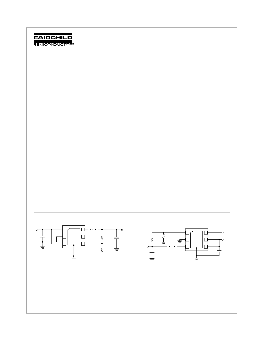
Typical Application
Figure 1. Typical Application
1
2
3
6
5
4
FB
PGND
SW
PV
IN
V
IN
EN
P1
(AGND)
L1
R2
R1
V
OUT
2 x 10
µF
3.3
µH
10
µF
10K
5K
1.2V (1A)
FAN2002
2 x 10
µF
10
µF
V
OUT
EN
SW
C
IN
C
OUT
1.2V (1A)
1
2
3
6
5
4
FB
PGND
V
IN
NC
P1
(AGND)
3.3
µH
R1
10K
5K
R2
FAN2001
2
www.fairchildsemi.com
FAN2001/FAN2002 Rev. 1.0.2
F
AN2001/F
AN2002 1A High-Efficienc
y Step-Do
wn DC-DC Con
ver
ter
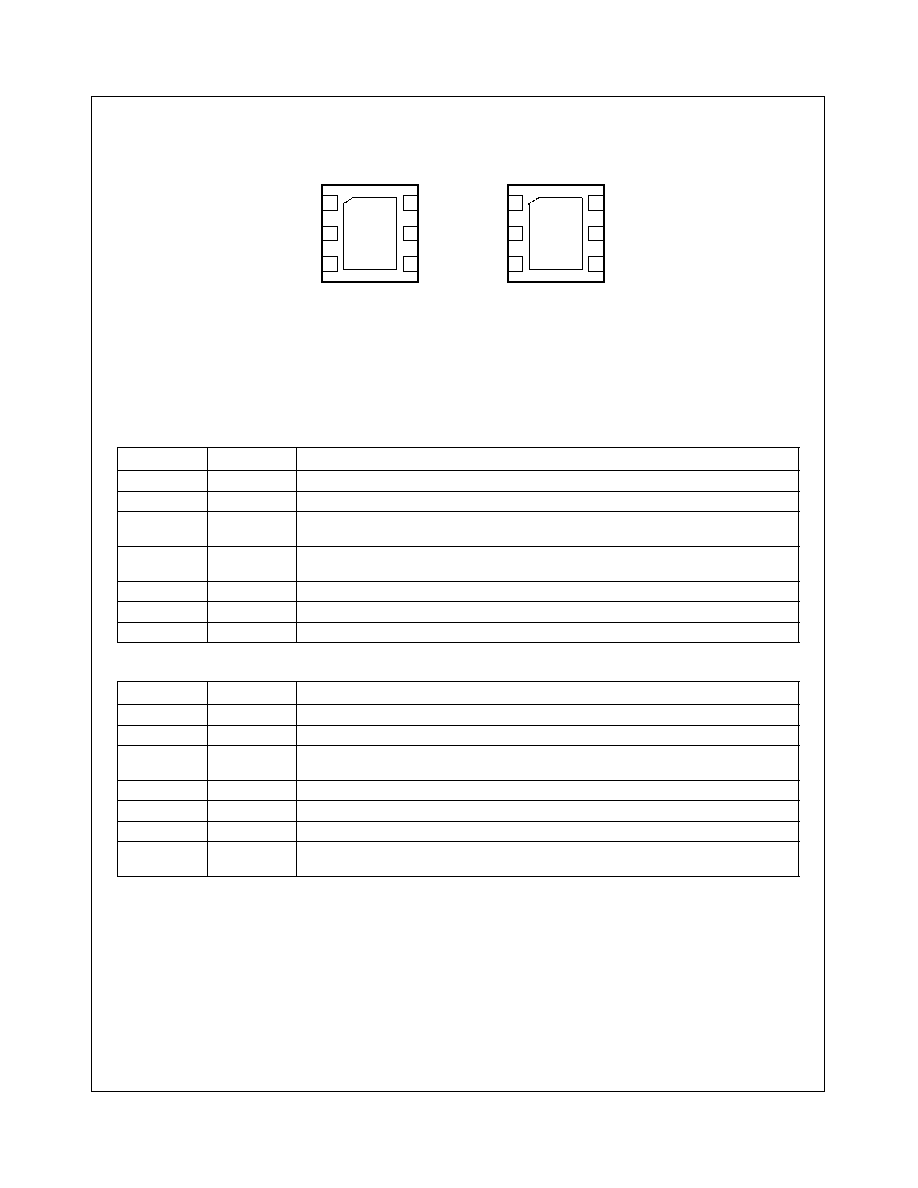
Pin Assignment
Figure 2. Pin Assignment
Pin Description
FAN2001 (3x3mm 6-Lead MLP)
FAN2002 (3x3mm 6-Lead MLP)
Pin No.
Pin Name
Pin Description
P1
AGND
Analog Ground.
P1 must be soldered to the PCB ground.
1
V
IN
Supply Voltage Input.
2
PGND
Power Ground.
This pin is connected to the internal MOSFET switches. This pin must be
externally connected to AGND.
3
EN
Enable Input.
Logic high enables the chip and logic low disables the chip, reducing the supply
current to less than 1µA. Do not float this pin.
4 FB
Feedback
Input.
Adjustable voltage option, connect this pin to the resistor divider.
5
NC
No Connection Pin.
6
SW
Switching Node.
This pin is connected to the internal MOSFET switches.
Pin No.
Pin Name
Pin Description
P1
AGND
Analog Ground.
P1 must be soldered to the PCB ground.
1
FB
Feedback Input.
Adjustable voltage option, connect this pin to the resistor divider.
2
PGND
Power Ground.
This pin is connected to the internal MOSFET switches. This pin must be exter-
nally connected to AGND.
3
SW
Switching Node.
This pin is connected to the internal MOSFET switches.
4 PV
IN
Supply Voltage Input.
This pin is connected to the internal MOSFET switches.
5
V
IN
Supply Voltage Input.
6
EN
Enable Input.
Logic high enables the chip and logic low disables the chip, reducing the supply
current to less than 1µA. Do not float this pin.
V
IN
PGND
EN
FB
SW
NC
1
2
3
6
5
4
P1
(AGND)
FB
PGND
SW
PV
IN
EN
V
IN
1
2
3
6
5
4
P1
(AGND)
Top View
3x3mm 6-Lead MLP
FAN2001
FAN2002
3
www.fairchildsemi.com
FAN2001/FAN2002 Rev. 1.0.2
F
AN2001/F
AN2002 1A High-Efficienc
y Step-Do
wn DC-DC Con
ver
ter
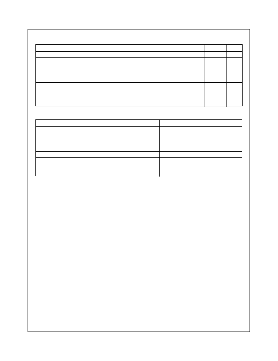
Absolute Maximum Ratings
(Note1)
Recommended Operating Conditions
Notes:
1. Stresses above those listed under "Absolute Maximum Ratings" may cause permanent damage to the device. This is a stress rating only and functional
operation of the device at these or any other conditions above those indicated in the operational section of this specification is not implied. Exposure
to absolute maximum rating conditions for extended periods may affect device reliability. Absolute maximum ratings apply individually only, not in
combination. Unless otherwise specified, all other voltages are referenced to AGND.
2. Junction to ambient thermal resistance,
JA
, is a strong function of PCB material, board thickness, thickness and number of copper planes, number of
via used, diameter of via used, available copper surface, and attached heat sink characteristics.
3. Using Mil Std. 883E, method 3015.7(Human Body Model) and EIA/JESD22C101-A (Charge Device Model).
4. Refer to the applications section for further details.
Parameter
Min
Max
Unit
V
IN
, PV
IN
-0.3
7
V
Voltage On Any Other Pin
-0.3
V
IN
V
Lead Soldering Temperature (10 seconds)
260
∞C
Junction Temperature
150
∞C
Storage Temperature
-65
150
∞C
Thermal Resistance-Junction to Tab
(
JC
)
,
3x3mm 6-lead MLP (Note 2)
8
∞C/W
Electrostatic Discharge Protection (ESD) Level (Note 3)
HBM
4
kV
CDM
1
Parameter
Min
Typ
Max
Unit
Supply Voltage Range
2.5
5.5
V
Output Voltage Range, Adjustable Version
0.8
V
IN
V
Output Current
1
A
Inductor (Note 4)
3.3
µ
H
Input Capacitor (Note 4)
10
µF
Output Capacitor (Note 4)
2 x 10
µF
Operating Ambient Temperature Range
-40
+85
∞C
Operating Junction Temperature Range
-40
+125
∞C
4
www.fairchildsemi.com
FAN2001/FAN2002 Rev. 1.0.2
F
AN2001/F
AN2002 1A High-Efficienc
y Step-Do
wn DC-DC Con
ver
ter
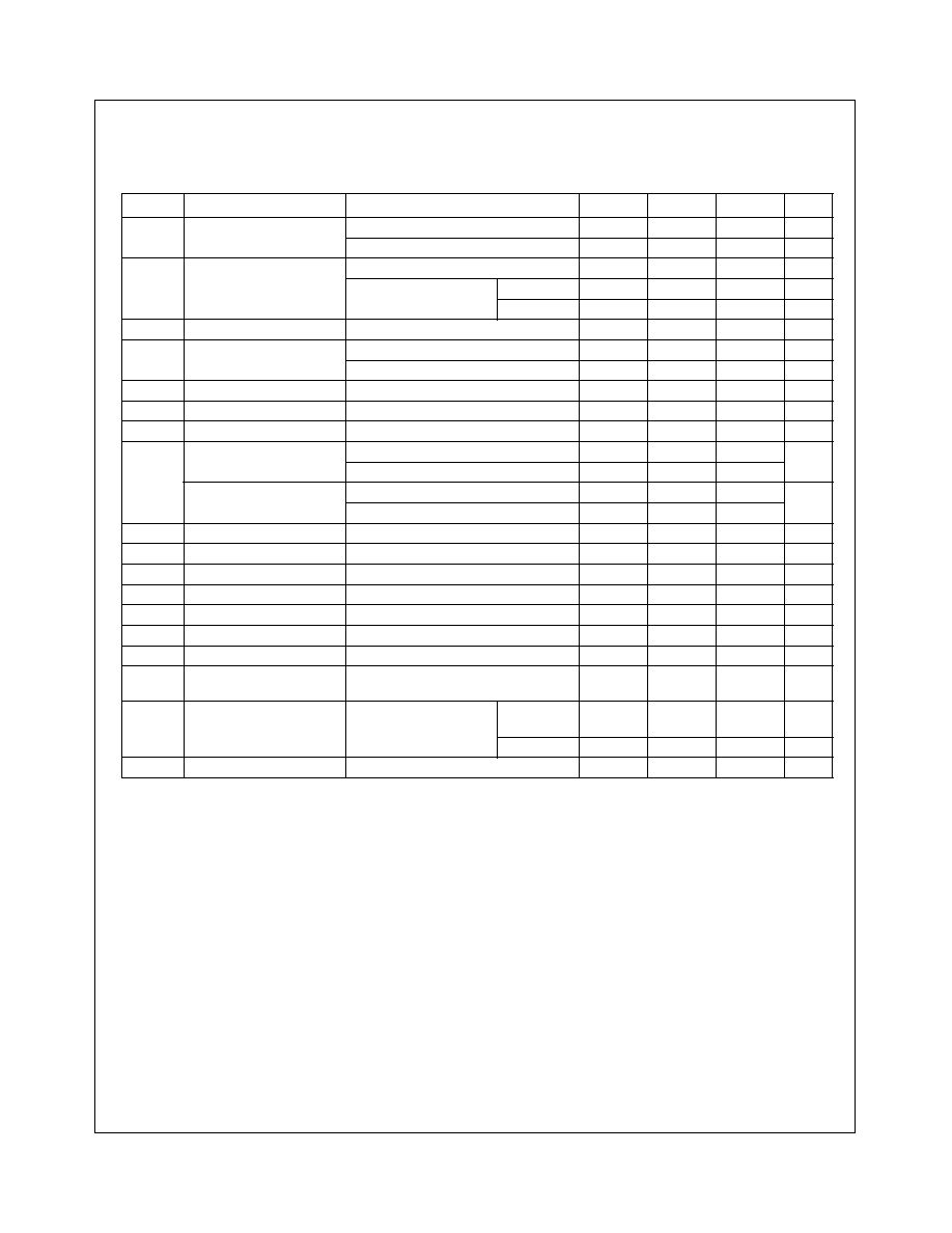
Electrical Characteristics
Notes:
5. Refer to the application section for further details.
6. For output voltages
1.2V a 40
µ
F output capacitor value is required to achieve a maximum output accuracy of 3% while operating in power save
mode (PFM mode).
V
IN
= V
OUT
+ 0.6V(min. 2.5V) to 5.5V, I
OUT
= 350mA, V
OUT
=1.2V, EN = V
IN
, T
A
= -40∞C to +85∞C,
Unless otherwise noted. Typical values are at T
A
= 25∞C.
Symbol
Parameter
Conditions
Min.
Typ.
Max.
Units
V
IN
Input Voltage
0 mA
I
OUT
600 mA
2.5
5.5
V
0 mA
I
OUT
1000 mA
2.7
5.5
V
I
Q
Quiescent Current
I
OUT
= 0mA, Device is not switching
20
35
µ
A
I
OUT
= 0mA, Device is
switching (Note 5)
R2 =10K
50
µ
A
R2 =100K
25
µ
A
Shutdown Supply Current
EN = GND
0.1
1
µ
A
Undervoltage Lockout
Threshold
V
IN
Rising
1.9
2.1
2.3
V
Hysteresis
150
mV
V
ENH
Enable High Input Voltage
1.3
V
V
ENL
Enable Low Input Voltage
0.4
V
I
EN
EN input bias current
EN = V
IN
or GND
0.01
0.1
µ
A
R
DS-ON
PMOS On Resistance
V
IN
= V
GS
= 5.5V
250
350
m
V
IN
= V
GS
= 2.5V
300
400
NMOS On Resistance
V
IN
= V
GS
= 5.5V
200
300
m
V
IN
= V
GS
= 2.5V
250
350
I
LIM
P-channel current limit
2.5V < V
IN
< 5.5V
1300
1500
2000
mA
Oscillator frequency
1000
1300
1500
KHz
I
lkg_(N)
N-channel leakage current
V
DS
= 5.5V
0.1
1
µ
A
I
lkg_(P)
P-channel leakage current
V
DS
= 5.5V
0.1
1
µ
A
Line regulation
I
OUT
10 mA
0.16
%/V
Load regulation
350 mA
I
OUT
1000 mA
0.15
%
Vref
Reference Voltage
0.8
V
Output DC Voltage Accuracy
(Note 6)
0 mA
I
OUT
1000 mA
-3
+3
%
Over-Temperature Protection PWM Mode Only
350 mA
I
OUT
1000 mA
Rising
Temperature
150
∞C
Hysteresis
20
∞C
Start-Up Time
I
OUT
= 1000 mA, C
OUT
= 20 µF
800
µS
5
www.fairchildsemi.com
FAN2001/FAN2002 Rev. 1.0.2
F
AN2001/F
AN2002 1A High-Efficienc
y Step-Do
wn DC-DC Con
ver
ter
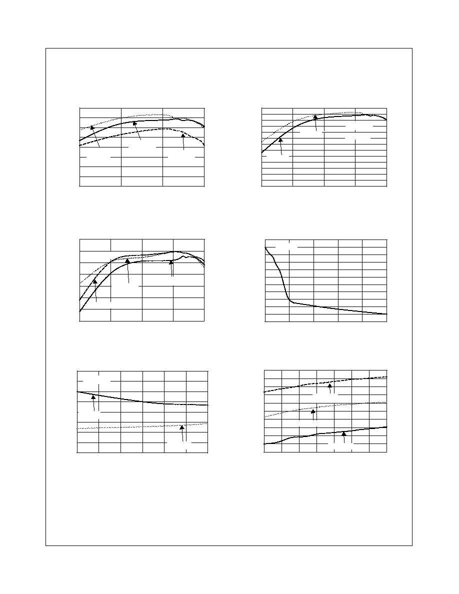
Typical Performance Characteristics
T
A
= 25∞C, C
IN
= 10µF, C
OUT
= 20µF, L = 3.3µH, R
2
= 10K
, unless otherwise noted.
1
10
100
1000
60
65
70
75
80
85
90
95
100
V
IN
= 5V
V
OUT
= 3.3V
V
IN
= 3.6V
V
OUT
= 1.2V
V
IN
= 3.6V
V
OUT
= 3V
0.1
1
10
100
1000
35
40
45
50
55
60
65
70
75
80
85
90
95
100
V
IN
= 5.5V
V
OUT
= 3.3V
V
IN
= 3.9V
0.1
1
10
100
1000
30
40
50
60
70
80
90
100
Load Current (mA)
Load Current (mA)
Load Current (mA)
Load Current (mA)
Efficiency (%)
Efficiency (%)
Efficiency (%)
Efficiency vs. Load Current
Efficiency vs. Load Current
Efficiency vs. Load Current
V
OUT
= 1.2V
V
IN
= 5.5V
V
IN
= 3. 6V
V
IN
= 2.5V
0
200
400
600
800
1000
1.192
1.194
1.196
1.198
1.200
1.202
1.204
1.206
1.208
1.210
1.212
1.214
Output Voltage (V)
Quiescent Current (
µ
A)
Oscillator Frequency (kHz)
V
IN
= 5V
Output Voltage vs. Load Current
2.5
3.0
3.5
4.0
4.5
5.0
5.5
0
10
20
30
40
50
60
70
80
Input Voltage (V)
R
2
= 100K
R
2
= 10K
Quiescent Current vs. Input Voltage
-40
-20
0
20
40
60
80
100
1200
1220
1240
1260
1280
1300
1320
1340
1360
1380
1400
Temperature (
∞C)
Frequency vs. Temperature
V
IN
= 2.5V
V
IN
= 3.6V
V
IN
= 5.5V
V
OUT
= 1. 2V
R
2
= 100K
R
2
= 100K