 | –≠–ª–µ–∫—Ç—Ä–æ–Ω–Ω—ã–π –∫–æ–º–ø–æ–Ω–µ–Ω—Ç: FAN4113 | –°–∫–∞—á–∞—Ç—å:  PDF PDF  ZIP ZIP |
Features at +1.2V
∑ 640
µA supply current per amplifier
∑ 36MHz gain bandwidth product
∑ Output voltage range: 0.06V to 1.10V
∑ Input voltage range: -0.4V to +0.2V
∑ 8V/
µs slew rate
∑ 12nV/
Hz input voltage noise
∑ Package option (SC70-5)
∑ Fully specified at +1.2V, +2.7V, and +5V supplies
Applications
∑ Cellular phones
∑ Personal data assistants
∑ A/D buffer
∑ DSP interface
∑ Smart card readers
∑ Portable test instruments
∑ Single cell NiCd/Ni MH powered systems
∑ Keyless entry
∑ Infrared receivers for remote controls
∑ Telephone systems
∑ Audio applications
Description
The FAN4113 is a low cost, voltage feedback amplifier that
consumes only 640
µA of supply current. The FAN4113 is
designed to operate from +1.2V to 5.5V (±2.75V) supplies.
The common mode voltage range extends below the negative
rail and the output provides rail-to-rail performance.
The FAN4113 is designed on a complementary bipolar
process and provides 36MHz of bandwidth and 8V/
µs of slew
rate at a low supply voltage of 1.2V. The combination of low
power, rail-to-rail performance, low voltage operation, and
tiny package options make the FAN4113 well suited for use
in personal electronics equipment such as cellular handsets,
pagers, PDAs, and other battery powered applications.
FAN4113
1.2V, 36MHz, Low Power Rail-to-Rail Amplifier
www.fairchildsemi.com
REV. 1 October 2001
+
-
FAN4113
R
f
0.01
µF
6.8
µF
Out
+In
+V
s
+
R
g
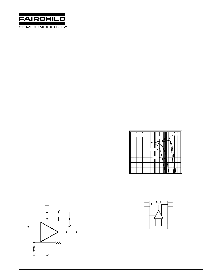
Typical Application
Non-Inverting Freq. Response, V
s
= 1.2V
Normalized Magnitude (1dB/div)
Frequency (MHz)
0.01
0.1
G = 10
1
10
100
G = 5
G = 1
G = 2
V
o
= 50mV
pp
Pin Assignments
-
+
1
2
3
Out
-V
s
+In
+V
s
-In
5
4

Absolute Maximum Ratings
Parameter
Min.
Max.
Unit
Supply Voltages
0
+6
V
Maximum Junction Temperature
≠
+175
∞C
Storage Temperature Range
-65
+150
∞C
Lead Temperature, 10 seconds
≠
+260
∞C
Operating Temperature Range, recommended
-40
+85
∞C
Input Voltage Range
-Vs -0.5 +Vs +0.5
V
ja for 5 load SC70
331.4∞C/W
Electrical Specifications
(T
c
= 25∞C, V
s
= +1.2V, G = 2, R
L
= 5k
to V
s
/2, R
f
= 5k
, V
o (DC)
= V
cc
/2; unless otherwise noted)
Parameter
Conditions
Min.
Typ.
Max.
Unit
AC Performance
-3dB Bandwidth
1
G = +2, V
o
= 50mV
pp
20
MHz
Full Power Bandwidth
G = +2, V
o
= 500mV
pp
9 MHz
Gain Bandwidth Product
36
MHz
Rise and Fall Time
200mV
pp
25 ns
Overshoot
200mV
pp
6 %
Slew Rate
500mV
pp
8 V/
µs
2nd Harmonic Distortion
0.5V
pp
, 500kHz
75
dBc
3rd Harmonic Distortion
0.5V
pp
, 500kHz
84
dBc
THD
0.5V
pp
, 500kHz
0.018
%
Input Voltage Noise
>100kHz
12
nV/
Hz
DC Performance
Input Offset Voltage
0.5
mV
Average Drift
2
µV/∞C
Input Bias Current
400
nA
Average Drift
2
nA/∞C
Input Offset Current
30
nA
Power Supply Rejection Ratio
DC
80
dB
Open Loop Gain
65
dB
Supply Current
640
µA
Input Characteristics
Input Resistance
25
M
Input Capacitance
1.8
pF
Input Common Mode Voltage Range
-0.4 to 0.2
V
Common Mode Rejection Ratio
72
dB
Output Characteristics
Output Voltage Swing
R
L
= 5k
to V
s
/2
0.05 to 1.11
V
R
L
= 1k
to V
s
/2
0.07 to 1.03
V
Output Current
±1.2
mA
Short Circuit Output Current
±1.8
mA
Power Supply Operating Range
1.2
1.2
5.5
V
Min/max ratings are based on product characterization and simulation. Individual parameters are tested as noted. Outgoing quality levels are
determined from tested parameters.
Notes:
1. For G = +1, Rf = 0.
DATA SHEET
FAN4113
2
REV. 1 October 2001

Electrical Specifications
(T
c
= 25∞C, V
s
= +2.7V, G = 2, R
L
= 5k
to V
s
/2, R
f
= 5k
, V
o (DC)
= V
cc
/2; unless otherwise noted)
Parameter
Conditions
Min.
Typ.
Max.
Unit
AC Performance
-3dB Bandwidth
1
G = +1, V
o
= 50mV
pp
42
MHz
G = +2, V
o
= 50mV
pp
20
MHz
Full Power Bandwidth
G = +2, V
o
= 500mV
pp
9 MHz
Gain Bandwidth Product
35
MHz
Rise and Fall Time
200mV
pp
25 ns
Settling Time to 1%
1V
pp
200
ns
Overshoot
200mV
pp
4 %
Slew Rate
1V
pp
8 V/
µs
2nd Harmonic Distortion
0.5V
pp
, 500kHz
75
dBc
3rd Harmonic Distortion
0.5V
pp
, 500kHz
84
dBc
THD
0.5V
pp
, 500kHz
0.018
%
Input Voltage Noise
>100kHz
12
nV/
Hz
DC Performance
Input Offset Voltage
2
-2.5
0.5
+2.5
mV
Average Drift
2
µV/∞C
Input Bias Current
2
400
800
nA
Average Drift
2
nA/∞C
Input Offset Current
30
nA
Power Supply Rejection Ratio
2
DC
66
80
dB
Open Loop Gain
70
dB
Supply Current
2
750
900
µA
Input Characteristics
Input Resistance
25
M
Input Capacitance
1.4
pF
Input Common Mode Voltage Range
-0.4 to 1.7
V
Common Mode Rejection Ratio
2
66
75
dB
Output Characteristics
Output Voltage Swing
R
L
= 5k
to V
s
/2
2
0.085 to 2.55 0.04 to 2.64
V
R
L
= 1k
to V
s
/2
0.07 to 2.56
V
Output Current
±9
mA
Short Circuit Output Current
±11
mA
Power Supply Operating Range
1.2
2.7
5.5
V
Min/max ratings are based on product characterization and simulation. Individual parameters are tested as noted. Outgoing quality levels are
determined from tested parameters.
Notes:
1. For G = +1, Rf = 0.
2. 100% tested at +25∞C.
FAN4113
DATA SHEET
REV. 1 October 2001
3

Electrical Specifications
(T
c
= 25∞C, V
s
= +5V, G = 2, R
L
= 5k
to V
s
/2, R
f
= 5k
, V
o (DC)
= V
cc
/2; unless otherwise noted)
Parameter
Conditions
Min.
Typ.
Max.
Unit
AC Performance
-3dB Bandwidth
1
G = +1, V
o
= 50mV
pp
36
MHz
G = +2, V
o
= 50mV
pp
20
MHz
Full Power Bandwidth
G = +2, V
o
= 500mV
pp
9 MHz
Gain Bandwidth Product
31
MHz
Rise and Fall Time
200mV
pp
25 ns
Settling Time to 1%
2V
pp
250
ns
Overshoot
200mV
pp
2 %
Slew Rate
2V
pp
8 V/
µs
2nd Harmonic Distortion
0.5V
pp
, 500kHz
75
dBc
3rd Harmonic Distortion
0.5V
pp
, 500kHz
84
dBc
THD
0.5V
pp
, 500kHz
0.018
%
Input Voltage Noise
>100kHz
12
nV/
Hz
DC Performance
Input Offset Voltage
0.5
mV
Average Drift
2
µV/∞C
Input Bias Current
400
nA
Average Drift
2
nA/∞C
Input Offset Current
30
nA
Power Supply Rejection Ratio
DC
80
dB
Open Loop Gain
70
dB
Supply Current
750
µA
Input Characteristics
Input Resistance
25
M
Input Capacitance
1.25
pF
Input Common Mode Voltage Range
-0.4 to 4.0
V
Common Mode Rejection Ratio
76
dB
Output Characteristics
Output Voltage Swing
R
L
= 5k
to V
s
/2
0.03 to 4.92
V
R
L
= 1k
to V
s
/2
0.07 to 4.79
V
Output Current
±9
mA
Short Circuit Output Current
±13
mA
Power Supply Operating Range
1.2
5
5.5
V
Min/max ratings are based on product characterization and simulation. Individual parameters are tested as noted. Outgoing quality levels are
determined from tested parameters.
Notes:
1. For G = +1, Rf = 0.
DATA SHEET
FAN4113
4
REV. 1 October 2001
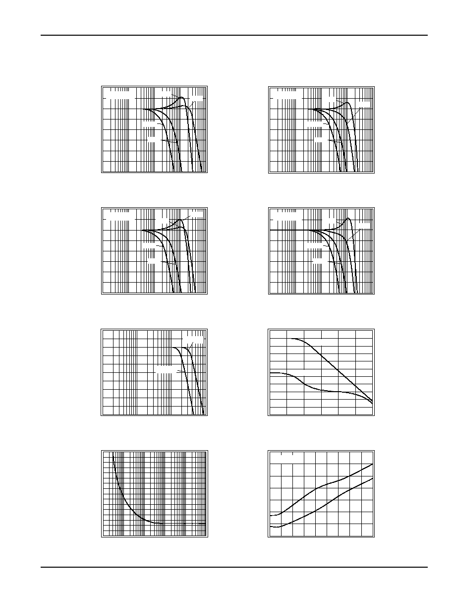
Typical Operating Characteristics
(T
c
= 25∞C, V
s
= +2.7V, G = 2, R
L
= 5k
to V
s
/2, R
f
= 5k
, V
o (DC)
= V
cc
/2; unless otherwise noted)
Non-Inverting Frequency Response
Normalized Magnitude (1dB/div)
Frequency (MHz)
0.01
0.1
G = 10
1
10
100
G = 5
G = 2
G = 1
V
o
= 50mV
pp
Inverting Frequency Response
Normalized Magnitude (1dB/div)
Frequency (MHz)
0.01
0.1
G = -10
1
10
100
G = -5
G = -1
G = -2
V
o
= 50mV
pp
Non-Inverting Freq. Response, V
s
= 1.2V
Normalized Magnitude (1dB/div)
Frequency (MHz)
0.01
0.1
G = 10
1
10
100
G = 5
G = 1
G = 2
V
o
= 50mV
pp
Inverting Freq. Response, V
s
= 1.2V
Normalized Magnitude (1dB/div)
Frequency (MHz)
0.01
0.1
G = -10
1
10
100
G = -5
G = -1
G = -2
V
o
= 50mV
pp
Large Signal Frequency Response
Magnitude (1dB/div)
Frequency (MHz)
0.01
0.1
1
10
V
o
= 1V
pp
V
o
= 2V
pp
Open Loop Gain & Phase vs. Frequency
Open Loop Gain (dB)
Frequency (Hz)
-30
-10
0
10
20
-200
-162
-124
-86
-48
-10
30
40
50
60
70
80
1k
10k
100k
1M
10M
100M
Ph
a
s
e (de
g
ree
s
)
|Gain|
-20
100
Phase
Input Voltage Noise
Voltage Noise (nV/
Hz)
Frequency (MHz)
0.001
0.01
0.1
1
0.0001
10
0
10
20
30
40
50
60
70
80
Harmonic Distortion vs. Frequency
Distortion (dBc)
Frequency (KHz)
100 200
300 400 500
600 700 800 900
2nd
3rd
1000
-95
-90
-85
-80
-75
-70
-65
-60
V
o
= 500mV
pp
FAN4113
DATA SHEET
REV. 1 October 2001
5