
www.fairchildsemi.com
REV. 1.0.0 Jul/15/05
Features
∑ Improved Noise Immunity
∑ Improved Load Line Accuracy
∑ TTL Compatible VID Inputs
∑ Fully Pin and Function compatible with existing
FAN5018 and ADP3180 Controllers
∑ Precision Multi-Phase DC-DC Core Voltage Regulation
≠ ±14mV Output Voltage Accuracy Over Temperature
∑ Differential Remote Voltage Sensing
∑ Selectable 2-, 3-, or 4-Phase Operation
∑ Selectable VRM9 or VRM10 Operation
∑ Up to 1MHz per Phase Operation (4MHz ripple
Frequency)
∑ Lossless Inductor Current Sensing for Loadline
Compensation
≠ External Temperature Compensation
∑ Accurate Loadline Programming (Meets Intel
Æ
VRM/VRD10.x CPU Specifications)
∑ Accurate Channel-Current Balancing for Thermal
Optimization and Layout Compensation
∑ Convenient 12V Supply Biasing
∑ 6-bit Voltage Identification (VID) Input
≠ .8375V to 1.600V in 12.5mV Steps
≠ Dynamic VID Capability with Fault-Blanking for
glitch-less Output voltage Changes
∑ Adjustable Over Current Protection with Programmable
Latch-Off Delay. Latch-Off Function may be Disabled
∑ Over-Voltage Protection ≠ Internal OVP Crowbar
Protection
∑ Package: 28L-TSSOP
Applications
∑ VRM/VRD 9.x and 10.x Computer DC/DC Converter
∑ High-Current, Low-Voltage DC/DC Rail
General Description
The FAN5018B is a multi-phase DC-DC controller for
implementing high-current, low-voltage, CPU core power
regulation circuits. It is part of a chipset that includes exter-
nal MOSFET drivers and power MOSFETS. The
FAN5018B drives up to four synchronous-rectified buck
channels in parallel. The multi-phase buck converter archi-
tecture uses interleaved switching to multiply ripple fre-
quency by the number of phases and reduce input and output
ripple currents. Lower ripple results in fewer components,
lower component cost, reduced power dissipation, and
smaller board area.
The FAN5018B features a high-bandwidth control loop to
provide optimal response to load transients. The FAN5018B
senses current using lossless techniques: Phase current is
measured through each of the output inductors. This current
information is summed, averaged and used to set the loadline
of the output via programmable "droop." The droop is tem-
perature compensated to achieve precise loadline character-
istics over the entire operating range. Additionally,
individual phase current is measured using the R
DS(ON)
of
the low-side MOSFETs. This information is used to dynam-
ically balance/steer per-phase current. The phase currents
are also summed and averaged for over-current detection.
Dynamic-VID technology allows on-the-fly VID changes
with controlled, glitch-less output. Additionally, short-circuit
protection, adjustable current limiting, over-voltage protec-
tion and power-good circuitry combine to ensure reliable and
safe operation. FAN5018B is specified over the commercial
temperature range of 0∞C to +85∞C and operates from a sin-
gle +12V supply which simplifies design. FAN5018B is
available in a 28L-TSSOP package.
Block Diagram
FAN5018B
V
IN
V
IN
1
4
V
OUT
3
2
FAN5009
FAN5009
FAN5018B
6-Bit VID Controller 2-4 Phase VR10.X Controller

FAN5018B
PRODUCT SPECIFICATION
2
REV. 1.0.0 Jul/15/05
Pin Assignments
Pin Definitions
Pin Number
Pin Name
Pin Function Description
1≠5
VID [4:0]
VID inputs. Determines the output voltage via the internal DAC. These inputs
comply to VRM10/VRD10 specifications for static and dynamic operation. All have
internal pull-ups (1.25V for VRM10 and 2.5V for VRM9) so leaving them open
results in logic high. Leaving VID[4:0] open results in a "No CPU" condition
disabling the PWM outputs.
6
VID5/SEL
VID5 Input/DAC Select. Dual function pin that is either the 12.5mV DAC LSB for
VRM10 or selects the VRM9 DAC codes when forced higher than Vtblsel(VRM9)
voltage. The truth table is as follows:
V
VID5/SEL
held > Vtblsel(VRM9); VRM9 DAC table is selected (See Table 3)
V
ViD5/SEL
< Vtblsel(VRM10); VRM10 DAC table is selected (See Table 2) and
V
ViD5/SEL
pin is used as VID5 input.
7
FBRTN
Feedback Return. Error Amp and DAC reference point.
8
FB
Feedback Input. Inverting input for Error Amp this pin is used for external
compensation. This pin can also be used to introduce DC offset voltage to the
output.
9
COMP
Error Amp output. This pin is used for external compensation.
10
PWRGD
Power Good output. This is an open-drain output that asserts when the output
voltage is within the specified tolerance. It is expected to be pulled up to an external
voltage rail.
11
EN
Enable. Logic signal that enables the controller when logic high.
12
DELAY
Soft-start and Current Limit Delay. An external resistor and capacitor sets the
softstart ramp rate and the over-current latch off delay.
13
RT
Switching Frequency Adjust. This pin adjusts the output PWM switching
frequency via an external resistor.
14
RAMPADJ
PWM Current Ramp Adjust. An external resistor to Vcc will adjust the amplitude of
the internal PWM ramp.
15
ILIMIT
Current Limit Adjust. An external resistor sets the current limit threshold for the
regulator circuit. This pin is internally pulled low when EN is low or the UVLO circuit
is active. It is also used to enable the drivers.
DELAY
VID4
VID3
VID2
VID1
VID0
COMP
CSCOMP
PWRGD
EN
CSSUM
RT
VCC
SW2
SW3
PWM3
PWM4
PWM1
GND
FBRTN
ILIMIT
FB
CSREF
RAMPADJ
1
2
3
4
5
6
7
8
9
10
11
12
13
14
28
27
26
25
24
23
22
21
20
19
18
17
16
15
FAN5018B
TSSOP-28
SW1
PWM2
SW4
VID5/SEL

PRODUCT SPECIFICATION
FAN5018B
REV. 1.0.0 Jul/15/05
3
16
CSREF
Current Sense Reference. Non-Inverting input of the current sense amp. Sense
point for the output voltage used for OVP and PWRGD.
17
CSSUM
Current Sense Summing node. Inverting input of the current sense amp.
18
CSCOMP
Current Sense Compensation node. Output of the current sense amplifier. This
pin is used, in conjunction with CSSUM to set the output droop compensation and
current loop response.
19
GND
Ground. Signal ground for the device.
20≠23
SW[4:1]
Phase Current Sense/Balance inputs. Phase-to-phase current sense and
balancing inputs. Unused phases should be left open.
24≠27
PWM[4:1]
PWM outputs. CMOS outputs for driving external gate driver such as the FAN5009.
Unused phases should be connected to Ground.
28
VCC
Chip Power. Bias supply for the chip. Connect directly to a +12V supply. Bypass
with a 1µF MLCC capacitor.
Pin Definitions
(continued)
Pin Number
Pin Name
Pin Function Description
FAN5018B
PRODUCT SPECIFICATION
4
REV. 1.0.0 Jul/15/05
Absolute Maximum Ratings
Absolute maximum ratings are the values beyond which the device may be damaged or have its useful life impaired. Func-
tional operation under these conditions is not implied.
Thermal Information
Recommended Operating Conditions
(See Figure 8)
Note:
1:
JA
is defined as 1 oz. copper PCB with 1 in
2
pad.
Parameter
Min.
Max.
Units
Supply Voltage: VCC to GND
-0.3
+15
V
Voltage on FBRTN pin
-0.3
+0.3
V
Voltage on SW1-SW4 (<250ns duration)
-5
+25
V
Voltage on SW1-SW4 (>=250ns duration)
-0.3
+15
V
Voltage on RAMPADJ, CSSUM
-0.3
VCC+0.3
V
Voltage on any other pin
-0.3
+5.5
V
Parameter
Min.
Typ
Max.
Units
Operating Junction Temperature (T
J
)
0
+150
∞C
Storage Temperature
≠65
+150
∞C
Lead Soldering Temperature, 10 seconds
+300
∞C
Vapor Phase, 60 seconds
+215
∞C
Infrared, 15 seconds
+220
∞C
Power Dissipation (P
D
) @ T
A
= 25∞C
2
W
Thermal Resistance (
JA
) (See Note 1)
50
∞C/W
Parameter
Conditions
Min.
Typ.
Max.
Units
Supply Voltage VCC
VCC to GND
10.2
12
13.8
V
Ambient Operating Temperature
0
+85
∞C
Operating Junction Temperature (T
J
)
0
+125

PRODUCT SPECIFICATION
FAN5018B
REV. 1.0.0 Jul/15/05
5
Electrical Specifications
(V
CC
= 12V, T
A
= 0∞C to +85∞C and FBRTN=GND, using circuit in Figure 1, unless otherwise noted.)
The
∑ denotes specifications which apply over the full operating temperature range.
Parameter
Symbol
Conditions
Min.
Typ.
Max.
Units
Error Amplifier
Output Voltage Range
V
COMP
∑
0.5
3.5
V
Accuracy
V
FB
Relative to DAC Setting,
referenced to FBRTN,
CSSUM = CSCOMP,
Test Circuit 3
VRM10
VRM9
∑
∑
-14
-17
+14
+17
mV
Line Regulation
V
FB
VCC=10V to 14V
0.05
%
Input Bias Current
I
FB
∑
-17
-15
-13
µA
FBRTN Current
I
FBRTN
∑
150
180
µA
Output Current
I
O(ERR)
FB forced to V
OUT
≠ 3%
300
500
µA
Gain Bandwidth Product
GBW
COMP = FB ( See Note 2)
20
MHz
DC Gain
C
COMP
= 10pF ( See Note 2)
77
dB
VID Inputs
Input Low Voltage
V
IL(VID)
VRM10
VRM9
∑
∑
0.4
0.8
V
V
Input High Voltage
V
IH(VID)
VRM10
VRM9
∑
∑
0.8
2.0
V
V
Input Current, VID Low
I
IL(VID)
VID(X) = 0V
∑
-30
-20
µA
Input Current, VID High
I
IH(VID)
VID(X) = 1.15V
∑
-2
2
µA
Pull-up Resistance
R
VID
Internal
∑
35
60
115
k
Internal Pull-up Voltage
VRM10
VRM9
∑
∑
1.0
2.2
1.15
2.4
1.26
2.6
V
V
VID Transition Delay
Time
2
VID Code Change to FB Change
∑
400
ns
"No CPU" Detection
Turn-off Delay Time
2
VID Code Change to 11111X to PWM
going low
∑
400
ns
VID Table Select
Vtblsel
To select VRM9 table
To select VRM10 table (becomes VID5)
∑
∑
4
3.5
V
V
Oscillator
Frequency
f
OSC
∑
200
4000
kHz
Frequency Variation
f
PHASE
T
A
= +25∞C, R
T
= 250k
, 4-Phase
T
A
= +25∞C, R
T
= 115k
, 4-Phase
T
A
= +25∞C, R
T
= 75k
, 4-Phase
∑
155
200
400
600
245
kHz
kHz
kHz
Output Voltage
V
RT
R
T
= 100k
to GND
∑
1.9
2.0
2.1
V
RAMPADJ Pin Accuracy
V
RAMPADJ
V
RAMPADJ
= Vdac = +2K ∑ (Vin≠Vdac)/
(Rr+2k) @ 20µA
∑
-50
+50
mV
RAMPADJ Input Current
I
RAMPADJ
Current into RAMPADJ pin
0
100
µA
Current Sense Amplifier
Offset Voltage
V
OS(CSA)
CSSUM≠CSREF, Test Circuit 1
∑
-3.0
+3.0
mV
Input Bias Current
I
BIAS(CSA)
∑
-50
+50
nA
Gain Bandwidth Product
GBW
COMP = FB ( See Note 2)
10
MHz
Notes:
1. All limits at operating temperature extremes are guaranteed by design, characterization and statistical quality control
2. Guaranteed by design ≠ NOT tested in production.
FAN5018B
PRODUCT SPECIFICATION
6
REV. 1.0.0 Jul/15/05
DC Gain
( See Note 2)
77
dB
Input Common Mode
Range
CSSUM and CSREF
∑
0
3
V
Positioning Accuracy
V
FB
COMP = FB, Test Circuit 2
∑
-84
-80
-76
mV
Output Voltage Range
I
CSCOMP
= ±100µA
∑
0.1
3.3
V
Output Current
I
O(CSA)
FB forced to V
OUT
≠ 3% Source/Sink
300
375
µA
Current Balance Circuit
Input Operating Range
V
SW(X)CM
∑
-600
+200
mV
Input Resistance
R
SW(X)
SW(X) = 0V
∑
20
30
40
k
Input Current
I
SW(X)
SW(X) = 0V
∑
-10
-7
-4
µA
Input Current Matching
I
SW(X)
SW(X) = 0V
∑
-5
+5
%
Current Limit Comparator
ILIMIT Output Voltage
Normal Mode
In Shutdown
V
ILIMIT(NM)
V
ILIMIT(SD)
R
ILIMIT
= 250k
I
ILIMIT
= -100µA
∑
∑
2.9
3
3.1
400
V
mV
Output Current, Normal
Mode
I
ILIMIT(NM)
R
ILIMIT
= 250k
12
µA
Maximum Output Current
V
IILIMIT
= 3V
∑
60
µA
Current Limit Threshold
Voltage
V
CL
V
CSREF
≠V
CSCOMP
, R
ILIMIT
= 250k
∑
105
125
150
mV
Current Limit Setting Ratio
V
CL
/I
ILIMIT
10.4
mV/µA
Latch-off Delay Threshold
V
DELAY
In Current Limit
∑
1.7
1.8
1.9
V
Latch-off Delay Time
t
DELAY
R
DELAY
= 250k
, C
DELAY
= 4.7nF
600
µs
Soft Start
Output Current,
Soft start Mode
I
DELAY(SS)
During Start-up, DELAY < 2.8V
∑
-25
-20
-15
µA
Soft Start Delay Time
T
DELAY(SS)
R
DELAY
= 250k
, C
DELAY
= 4.7nF,
VID = 011111 (1.475V)
400
µs
Enable Input
Input Low Voltage
V
IL(EN)
∑
0.4
V
Input High Voltage
V
IH(EN)
∑
0.8
V
Input Current, EN Low
I
IL(EN)
EN = 0V
∑
-1
1
µA
Input Current, EN High
I
IH(EN)
EN = 1.25V
∑
10
25
µA
Power Good Comparator
Under voltage Threshold
V
PWRGD(UV)
Relative to DAC Output
∑
-325
-250
-200
mV
Over voltage Threshold
V
PWRGD(OV)
Relative to DAC Output
∑
180
300
400
mV
Output Low Voltage
V
OL(PWRGD)
I
PWRGD(SINK)
= 4mA
∑
225
400
mV
Electrical Specifications
(continued)
(V
CC
= 12V, T
A
= 0∞C to +85∞C and FBRTN=GND, using circuit in Figure 1, unless otherwise noted.)
The
∑ denotes specifications which apply over the full operating temperature range.
Parameter
Symbol
Conditions
Min.
Typ.
Max.
Units
Notes:
1. All limits at operating temperature extremes are guaranteed by design, characterization and statistical quality control
2. Guaranteed by design ≠ NOT tested in production.
PRODUCT SPECIFICATION
FAN5018B
REV. 1.0.0 Jul/15/05
7
Power Good Delay Time
Initial Start Up
VID Code Changing
VID Code Static
∑
1
100
250
200
10
ms
µs
ns
Crowbar Trip Point
V
CROWBAR
Relative to Nominal DAC Output
∑
180
300
400
mV
Crowbar Reset Point
Relative to FBRTN
∑
570
700
830
mV
Crowbar Delay Time
VID Code Changing
VID Code Static
t
CROWBAR
Over voltage to PWM Going Low
∑
100
250
400
500
600
µs
ns
PWM Outputs
Output Voltage Low
V
OL(PWM)
I
PWM(SINK)
= 400µA
∑
160
500
mV
Output Voltage High
V
OH(PWM)
I
PWM(SOURCE)
= 400µA
∑
4
5
5.5
V
Input Supply
DC Supply Current
EN = Logic High
∑
5
10
mA
UVLO Threshold
V
UVLO
Vcc Rising (Vcc = 12V input)
∑
6.5
6.9
8.1
V
UVLO Hysteresis
∑
0.7
V
UVLO Threshold
Falling
∑
5.6
7.1
Electrical Specifications
(continued)
(V
CC
= 12V, T
A
= 0∞C to +85∞C and FBRTN=GND, using circuit in Figure 1, unless otherwise noted.)
The
∑ denotes specifications which apply over the full operating temperature range.
Parameter
Symbol
Conditions
Min.
Typ.
Max.
Units
Notes:
1. All limits at operating temperature extremes are guaranteed by design, characterization and statistical quality control
2. Guaranteed by design ≠ NOT tested in production.

FAN5018B
PRODUCT SPECIFICATION
8
REV. 1.0.0 Jul/15/05
Internal Block Diagram
Phase
Current
Balancing
Circuit
VID
DAC
REF
Current
Limit
Circuit
Oscillator
UVLO
Shutdown
& Bias
11
28
19
13
14
CMP
Soft
Start
2/3/4 Phase Driver
Logic
EN
RESET
SET
RESET
RESET
RESET
CURRENT
LIMIT
CROWBAR
12
CMP
CMP
CMP
CSA
Error
Amp
24
25
26
27
20
21
22
23
+
-
15
7
6
5
4
3
2
1
18
16
17
10
EN
8
9
DELAY
VID4 VID3 VID2
VID1 VID0 VID5
COMP
PWRGD
EN
RT
FBRTN
FB
RAMPADJ
CSCOMP
CSSUM
VCC
SW2
SW3
PWM3
PWM4
PWM1
GND
ILIMIT
CSREF
SW1
PWM2
SW4
Delay
CMP
CMP
DAC
-250mV
CSREF
DAC
+150mV
2K
3.75V
Sel VRM9 Table
PRODUCT SPECIFICATION
FAN5018B
REV. 1.0.0 Jul/15/05
9
Typical Characteristics
Test Circuits
TPC 1. Master Clock Frequency
TPC 2. Supply Current vs. Master Clock Frequency
3.5
4
3
2.5
2
1.5
1
0.5
0
100
0
200
RESISTOR'S RT VALUE (k
)
MASTER CLOCK FREQUENCY (MHz)
300
400
5.2
5.3
5.1
5.0
4.9
4.8
4.7
4.6
1.0
0
2.0
MASTER CLOCK FREQUENCY (MHz)
SUPPLY CURRENT (mA)
3.0
4.0
0.5
1.5
2.5
3.5
T
A
= 25 C
4-Phase Operation
VCC
28
18
19
17
16 CSREF
CSSUM
CSCOMP
GND
CSA
100nF
39k
1k
1V
+12V
40
CSCOMP≠1V
V
OS
=
Test Circuit 1. Current Sense Amplifier V
OS
VCC
28
18
19
17
16
CSREF
CSSUM
CSCOMP
GND
CSA
100nF
200k
1V
+12V
9
8
10k
FB
COMP
200k
80mV
VID
FB
V
FB
V
-
=
Test Circuit 2. Voltage
Positioning
VID4
VID0
VID1
VID2
VID3
VID5
FAN5018B
VCC
1
VID4
8
11
10
9
12
14
13
6
5
4
7
3
2
28
21
18
19
20
17
15
16
23
24
25
22
26
27
RAMPADJ
RT
DELAY
EN
PWRGD
COMP
FB
FBRTN
VID5
VID0
VID1
VID2
VID3
ILIMIT
CSREF
CSSUM
CSCOMP
GND
SW4
SW3
SW2
SW1
PWM4
PWM3
PWM2
PWM1
250k
100nF
4.7nF
250k
20k
1
F
100nF
+12V
1k
Test Circuit 3. Closed Loop Output Voltage Accuracy
FAN5018B
PRODUCT SPECIFICATION
10
REV. 1.0.0 Jul/15/05
Application Circuit
Figure
1. Typic
a
l
Application ≠
3
-
phase,
65A (DC),
7
4
A (Peak) VRD/VRM10 Des
i
gn
U1 FAN500
9
4
6
2
3
8
1
5
7
HDRV
VCC
PGND
BOOT
SW
LDRV
PWM
OD
+12V
U4 FAN5018B
VCC
1
VID4
8
11
10
9
12
14
13
6
5
4
7
3
2
28
21
18
1
9
20
17
15
16
23
24
25
22
26
27
RAMPADJ
RT
DELAY
EN
PWRGD
COMP
FB
FBRTN
VID5/SEL
VID0
VID1
VID2
VID3
ILIMIT
CSREF
CSSUM
CSCOMP
GND
SW4
SW3
SW2
SW1
PWM4
PWM3
PWM2
PWM1
Q4
L1
Q5
Q1
C
X
Vcc CORE
0.8375V - 1.600V
74A DC,
9
3A Peak
C
IN
+12V
C
DLY
R
TH
*
R
T
R
DLY
C
FB
R
A
C
A
R
B
C
B
C
CS
R
CS1
R
SW1
R
SW3
R
SW2
R
CS2
R
PH1
R
PH2
R
PH3
C1
C4
C8
R1
9
C12
4
6
2
3
8
1
5
7
HDRV
VCC
PGND
BOOT
SW
LDRV
PWM
OD
Q6
L2
Q7
Q2
+12V
C2
C5
C
9
R20
C13
4
6
2
3
8
1
5
7
HDRV
VCC
PGND
BOOT
SW
LDRV
PWM
OD
Q8
L3
Q
9
Q3
+12V
C3
C6
C10
R21
C14
R
LIM
C7
R
R
R1
R5
L4
V
IN
V
IN
V
IN
PWRGD
EN
C
Z
R
B1
U3 FAN500
9
U2 FAN500
9
Note:
The design shown in this datasheet should be used as a reference only. Please contact your Fairchild sales representative for t
he latest information.

PRODUCT SPECIFICATION
FAN5018B
REV. 1.0.0 Jul/15/05
11
Bill of Materials
Table 1. FAN5018B VRM/VRD10 Application Bill of Materials for Figure 1
Note:
The design shown in this datasheet should be used as a reference only. Please contact your Fairchild sales representative
for the latest information.
Ref
Qty
Description
Manufacturer/Number
U4
1 VR10,
Multi-Phase
Controller Fairchild
FAN5018B
U1≠3
3
Sync MOSFET Driver, 12V/12V Fairchild
FAN5009
Q1≠3
3
N-MOSFET, 30V, 50A, 8m
Fairchild
FDD6696
Q4≠9
6
N-MOSFET, 30V, 75A, 5m
Fairchild
FDD6682
L1≠3
3
Inductor, 650nH, 26A, 1.6m
Micrometals T50-8B/90, 5T, 16AWG
L4
1
Inductor, 630nH, 15A, 1.7m
Inter-Technical
AK1418160052A-R63M
R1
1 10
, 5%
R
R
R
DLY
, R
T
3 301k
, 1%
R5
1 15.0k
, 1%
R
PH1≠3
3
100k
, 1%
R
A
, R
CS2
2 24.9k
, 1%
R
B1
1 10
, 1%
R
B
1 1.33k
, 1%
R
SW1≠3
3 0
, 5%
R
CS1
1 37.4k
, 1%
R
LIM
1 200k
, 1%
R19≠21
3 1.5
, 5%
R
TH
1
NTC Thermistor, 100k
, 5%
Panasonic ERT-J1V V104J
C1≠7
7
1.0µF, 25V, 10% X7R
C8≠10
3
0.1µF, 50V, 10% X7R
C12≠14, C
CS
4
4700pF, 25V, 10% X7R
C
DLY
1
0.047µF, 25V, 10% X7R
C
B
1
2200pF, 25V, 10% X7R
C
A
1
470pF, 50V, 10% X7R
C
FB
1
100pF, 50V, 5% NPO
C
X
8
820µF, 2.5V, 20% 7m
, POLY
Fujitsu FP-2R5RE821M
C
Z
22
10µF, 6.3V, 20% X5R
C
IN
6
470µF, 16V, 20%, 36m
, Alum-Elec
Rubycon 16MBZ470M

FAN5018B
PRODUCT SPECIFICATION
12
REV. 1.0.0 Jul/15/05
Table 2. VRM10 VID Codes
VID4
VID3
VID2
VID1
VID0
VID5
V
OUT
(nominal)
1
1
1
1
1
X
No CPU
0
1
0
1
0
0
0.8375 V
0
1
0
0
1
1
0.8500 V
0
1
0
0
1
0
0.8625 V
0
1
0
0
0
1
0.8750 V
0
1
0
0
0
0
0.8875 V
0
0
1
1
1
1
0.9000 V
0
0
1
1
1
0
0.9125 V
0
0
1
1
0
1
0.9250 V
0
0
1
1
0
0
0.9375 V
0
0
1
0
1
1
0.9500 V
0
0
1
0
1
0
0.9625 V
0
0
1
0
0
1
0.9750 V
0
0
1
0
0
0
0.9875 V
0
0
0
1
1
1
1.0000 V
0
0
0
1
1
0
1.0125 V
0
0
0
1
0
1
1.0250 V
0
0
0
1
0
0
1.0375 V
0
0
0
0
1
1
1.0500 V
0
0
0
0
1
0
1.0625 V
0
0
0
0
0
1
1.0750 V
0
0
0
0
0
0
1.0875 V
1
1
1
1
0
1
1.1000 V
1
1
1
1
0
0
1.1125 V
1
1
1
0
1
1
1.1250 V
1
1
1
0
1
0
1.1375 V
1
1
1
0
0
1
1.1500 V
1
1
1
0
0
0
1.1625 V
1
1
0
1
1
1
1.1750 V
1
1
0
1
1
0
1.1875 V
1
1
0
1
0
1
1.2000 V
1
1
0
1
0
0
1.2125 V
1
1
0
0
1
1
1.2250 V
1
1
0
0
1
0
1.2375 V
1
1
0
0
0
1
1.2500 V
1
1
0
0
0
0
1.2625 V
1
0
1
1
1
1
1.2750 V
1
0
1
1
1
0
1.2875 V
1
0
1
1
0
1
1.3000 V
1
0
1
1
0
0
1.3125 V
1
0
1
0
1
1
1.3250 V

PRODUCT SPECIFICATION
FAN5018B
REV. 1.0.0 Jul/15/05
13
1
0
1
0
1
0
1.3375 V
1
0
1
0
0
1
1.3500 V
1
0
1
0
0
0
1.3625 V
1
0
0
1
1
1
1.3750 V
1
0
0
1
1
0
1.3875 V
1
0
0
1
0
1
1.4000 V
1
0
0
1
0
0
1.4125 V
1
0
0
0
1
1
1.4250 V
1
0
0
0
1
0
1.4375 V
1
0
0
0
0
1
1.4500 V
1
0
0
0
0
0
1.4625 V
0
1
1
1
1
1
1.4750 V
0
1
1
1
1
0
1.4875 V
0
1
1
1
0
1
1.5000 V
0
1
1
1
0
0
1.5125 V
0
1
1
0
1
1
1.5250 V
0
1
1
0
1
0
1.5375 V
0
1
1
0
0
1
1.5500 V
0
1
1
0
0
0
1.5625 V
0
1
0
1
1
1
1.5750 V
0
1
0
1
1
0
1.5875 V
0
1
0
1
0
1
1.6000 V
Table 2. VRM10 VID Codes
(continued)
VID4
VID3
VID2
VID1
VID0
VID5
V
OUT
(nominal)

FAN5018B
PRODUCT SPECIFICATION
14
REV. 1.0.0 Jul/15/05
Table 3. VRM9 VID Codes
VID4
VID3
VID2
VID1
VID0
V
OUT
(nominal)
1
1
1
1
1
No CPU
1
1
1
1
0
1.100 V
1
1
1
0
1
1.125 V
1
1
1
0
0
1.150 V
1
1
0
1
1
1.175 V
1
1
0
1
0
1.200 V
1
1
0
0
1
1.225 V
1
1
0
0
0
1.250 V
1
0
1
1
1
1.275 V
1
0
1
1
0
1.300 V
1
0
1
0
1
1.325 V
1
0
1
0
0
1.350 V
1
0
0
1
1
1.375 V
1
0
0
1
0
1.400 V
1
0
0
0
1
1.425 V
1
0
0
0
0
1.450 V
0
1
1
1
1
1.475 V
0
1
1
1
0
1.500 V
0
1
1
0
1
1.525 V
0
1
1
0
0
1.550 V
0
1
0
1
1
1.575 V
0
1
0
1
0
1.600 V
0
1
0
0
1
1.625V
0
1
0
0
0
1.650V
0
0
1
1
1
1.675V
0
0
1
1
0
1.700V
0
0
1
0
1
1.725V
0
0
1
0
0
1.750V
0
0
0
1
1
1.775V
0
0
0
1
0
1.800V
0
0
0
0
1
1.825V
0
0
0
0
0
1.850V

PRODUCT SPECIFICATION
FAN5018B
REV. 1.0.0 Jul/15/05
15
General Description
Note: The information in this section is intended to assist
users in their design and understanding of the FAN5018B
functionality. For clarity and ease of understanding, device
parameters have been included in the text. In the event there
are discrepancies between values stated in this section and
the actual specification tables, the specification tables shall
be deemed correct.
Theory of Operation
The FAN5018B combines a multi-mode, fixed-frequency
PWM control with multi-phase logic outputs for use in 2, 3
and 4 phase synchronous buck CPU core supply power con-
verters. If VID5 is pulled up to a voltage greater than
VTBLSEL, then the DAC code corresponds to VRM9.
Multi-phase operation is important for producing the high
currents and low voltages demanded by today's micropro-
cessors. Handling the high currents in a single-phase con-
verter would place high thermal demands on the components
in the system, such as the inductors and MOSFETs. The
internal 6-bit VID DAC conforms to Intel's VRD/VRM 10
specifications.
The multi-mode control of the FAN5018B ensures a stable,
high-performance topology for:
∑ Balancing currents and thermals between phases
∑ High speed response at the lowest possible switching
frequency and output decoupling
∑ Minimizing thermal switching losses due to lower
frequency operation
∑ Tight load line regulation and accuracy
∑ High current output from having up to 4 phase operation
∑ Reducing output ripple due to multi-phase cancellation
∑ PC board layout noise immunity
∑ Ease of use and design due to independent component
selection
∑ Flexibility in operation for tailoring design to low cost or
high performance
Number of Phases
The number of operational phases and their phase relation-
ship is determined by internal circuitry which monitors the
PWM outputs. Normally, the FAN5018B operates as a 4-
phase PWM controller. Grounding the PWM4 pin programs
a 3-phase operation; grounding the PWM3 and PWM4 pins
programs a 2-phase operation.
When the FAN5018B is initially enabled, the controller out-
puts a voltage on PWM3 and PWM4 of approximately
550mV. An internal comparator checks each pin's voltage
versus a threshold of 400mV. If the pin is grounded, then it
will be below the threshold and the phase will be disabled.
The output impedance of the PWM pin is approximately
5k
. Any external pull-down resistance connected to the
PWM pin should not be less than 25k
to ensure proper
operation. The phase detection is made prior to starting nor-
mal operation. After this time, if the PWM output was not
grounded, then it will operate normally. If the PWM output
was grounded, then it will remain off.
The PWM outputs become logic-level output devices once
normal operation starts, and are intended for driving external
gate drivers. Since each phase is monitored independently,
operation approaching 100% duty cycle is possible. Also,
more than one output can be on at a time for overlapping
phases.
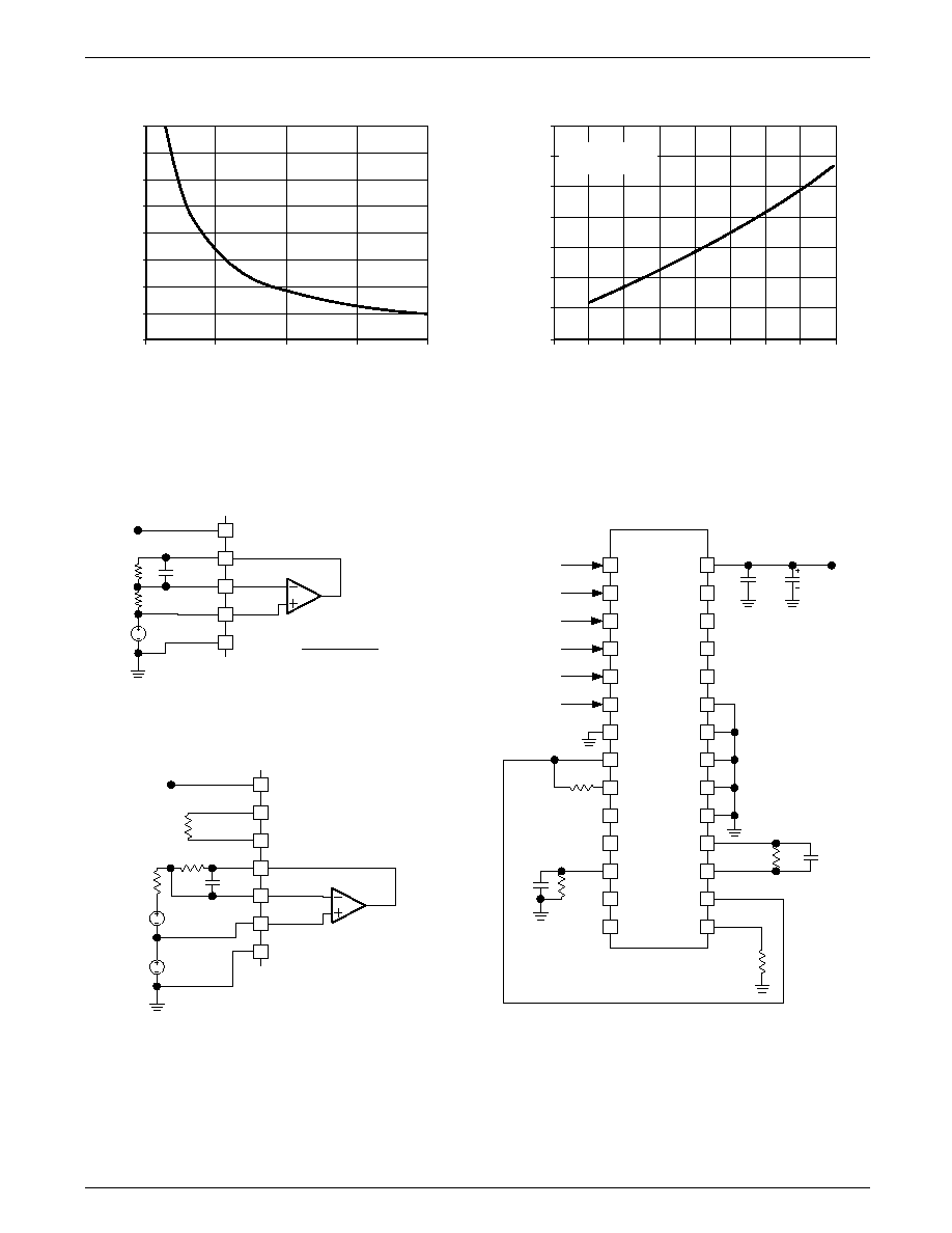
Master Clock Frequency
The clock frequency of the FAN5018B is set with an exter-
nal resistor connected from the RT pin to ground. The fre-
quency follows the graph shown in TPC 1. To determine the
frequency per phase, the clock is divided by the number of
phases in use. If PWM4 is grounded, then divide the master
clock by 3 and if both PWM3 and 4 are grounded, then
divide by 2. If all phases are in use, divide by 4.
Output Voltage Differential Sensing
The FAN5018B provides a high accuracy VID DAC and
error-amplifier to maintain a ±14 mV output setpoint toler-
ance over temperature. Output voltage is differentially
sensed between the FB and FBRTN pins. FB should be con-
nected through a resistor to the regulation point, usually the
remote sense pin of the microprocessor. FBRTN should be
connected directly to the remote sense ground point. The
internal VID DAC and precision reference are referenced to
FBRTN, which has a typical current of 150µA, to allow
accurate remote sensing. The internal error amplifier com-
pares the output of the DAC to the FB pin to regulate the out-
put voltage.
Output Current Sensing
The FAN5018B provides a dedicated current sense amplifier
(CSA) to monitor the total output current for proper voltage
positioning versus load current and for current limit detec-
tion. Sensing the load current at the output gives the total
average current being delivered to the load, which is an
inherently more accurate method than peak current detection
or sampling the current across a sense element such as the
low side MOSFET. There are several ways of configuring
this amplifier depending on the objectives of the system:
∑ Output inductor DCR sensing without thermistor for
lowest cost
∑ Output inductor DCR sensing with thermistor for
improved accuracy with tracking of inductor temperature
∑ Sense resistors for highest accuracy measurements
The positive input of the CSA is connected to the CSREF
pin, which is connected to the output voltage. The inputs to
the amplifier are summed together through resistors from the
sensing element (such as the switch node side of the output
inductors) to the inverting input, CSSUM. The feedback
resistor between CSCOMP and CSSUM sets the gain of the

FAN5018B
PRODUCT SPECIFICATION
16
REV. 1.0.0 Jul/15/05
amplifier, and a filter capacitor is placed in parallel with this
resistor. The amplifier's gain is programmable by adjusting
the feedback resistor to set the load line required by the
microprocessor. The current information is then given as the
difference of CSREF ≠CSCOMP. This difference signal is
used internally to offset the VID DAC for voltage position-
ing and as a differential input for the current limit compara-
tor.
To provide the best accuracy for the current sensing, the
CSA is designed to have a low offset input voltage. Also,
external resistors determine the sensing gain so that it can be
made extremely accurate and flexible.
Active Impedance Control Mode
For controlling the output voltage droop as a function of
output current, the current sense amplifier (CSA) creates a
voltage signal proportional to the total inductor currents.
External components determine the ratio of this voltage to
the output current to allow it to be adjusted to set the
required load line. Inside the chip the CSA output voltage is
subtracted from the DAC voltage which then is used for the
reference to the error amplifier. As the output current
increases the reference to the error amp decreases causing
the output voltage to decrease accordingly.
Current Control Mode and Thermal Balance
The FAN5018B has individual inputs for each phase which
are used for monitoring the current in each phase. This infor-
mation is combined with an internal ramp to create a current
balancing feedback system that is optimized for initial cur-
rent balance accuracy and dynamic thermal balancing during
operation. This current balance information is independent
of the average output current information used for position-
ing described previously.
The magnitude of the internal ramp can be set to optimize
the transient response of the system. It also monitors the sup-
ply voltage for feed-forward control for changes in the sup-
ply. A resistor connected from the power input voltage to the
RAMPADJ pin determines the slope of the internal PWM
ramp. Detailed information about programming the ramp is
given in the Application Information section.
External resistors can be placed in series with individual
phases to create an intentional current imbalance if desired,
such as when one phase may have better cooling and can
support higher currents. Resistors R
SW1
through R
SW4
(see the typical application circuit in Figure 4) can be used
for adjusting FET thermal and current balance. Zero ohm
placeholder resistors should be provided in the initial layout
to allow the phase balance to be adjusted during design fine
tuning.
To increase the current in any given phase, make R
SW
for
that phase larger (make R
SW
= 0 for the hottest phase and do
not change during balancing). Increasing R
SW
to only 500
will substantially increase the phase current. Increase each
R
SW
value by small amounts to achieve balance,
starting with the coolest phase first.
Voltage Control Mode
The voltage-mode control loop uses a high gain-bandwidth
voltage mode error amplifier. The control input voltage to
the positive input is set via the VID 6-bit logic code, accord-
ing to the voltages listed in Table 1. This voltage is also off-
set by the droop voltage for active positioning of the output
voltage as a function of current, commonly known as active
voltage positioning. The output of the amplifier is the COMP
pin, which sets the termination voltage for the internal PWM
ramps.
The negative input (F
B
) is tied to the output sense location
with a resistor R
B
and is used for sensing and controlling the
output voltage at this point. A current source from the F
B
pin
flowing through R
B
is used for setting the no-load offset
voltage from the VID voltage. The no-load voltage will be
negative with respect to the VID DAC. The main loop com-
pensation is incorporated in the feedback network between
FB and COMP.
Soft-Start
The power-on ramp up time of the output voltage is set with
a capacitor and resistor in parallel from the DELAY pin to
ground. The RC time constant also determines the current
limit latch off time as explained in the following section. In
UVLO or when EN is a logic low, the DELAY pin is held at
ground. After the UVLO threshold is reached and EN is a
logic high, the DELAY cap is charged up with an internal
20µA current source. The output voltage follows the ramp-
ing voltage on the DELAY pin, limiting the inrush current.
The soft-start time depends on the value of VID DAC and
C
DLY
, with a secondary effect from R
DLY
. Refer to the Appli-
cation Information section for detailed information on set-
ting C
DLY
.
If EN is taken low or VCC drops below UVLO, the DELAY
cap is reset to ground to be ready for another soft start cycle.
Figure 1 shows a typical start-up sequence for the
FAN5018B.
Over Current Limit and Latch-off Protection
The FAN5018B compares a programmable current limit set
point to the voltage from the output of the current sense
amplifier. The level of current limit is set with the resistor
from the ILIMIT pin to ground. During normal operation,
the voltage on ILIMIT is 3V. The current through the exter-
nal resistor is internally scaled to give a current limit thresh-
old of approximately 10.4mV/µA. If the difference in
voltage between CSREF and CSCOMP rises above the cur-
rent limit threshold, the internal current limit amplifier will
control the internal COMP voltage to maintain the average
output current at the limit.
PRODUCT SPECIFICATION
FAN5018B
REV. 1.0.0 Jul/15/05
17
After the limit is reached, the 3V pull-up on the DELAY pin
is disconnected, and the external delay capacitor is dis-
charged through the external resistor. A comparator monitors
the DELAY voltage and shuts off the controller when the
voltage drops below 1.8V. Therefore, the RC time constant
discharging from 3V to 1.8V sets the current limit latch off
delay time. The Application Information section discusses
the selection of C
DLY
and R
DLY
.
Because the controller continues to cycle the phases during
the latch-off delay time, if the short is removed before the
1.8V threshold is reached, the controller will return to nor-
mal operation. The recovery characteristic depends on the
state of PWRGD. If the output voltage is within the PWRGD
window, the controller resumes normal operation. However,
if a short circuit has caused the output voltage to drop below
the PWRGD threshold, then a soft-start cycle is initiated.
The latch-off function can be reset by either cycling VCC to
the FAN5018B, or by cycling the Enable pin low for a short
time. To disable the short circuit latch off function, the
external resistor to ground should be left open, and a 1M
resistor should be connected from VCC to the DELAY pin.
This prevents the DELAY capacitor from discharging, so the
1.8V threshold is never reached. The resistor will have an
impact on the soft-start time because the current through it
will add to the internal 20µA current source.
During start-up when the output voltage is below 200mV, a
secondary current limit is active. This is necessary because
the voltage swing of CSCOMP cannot go below ground.
This secondary current limit controls the internal COMP
voltage to the PWM comparators to 2V. This will limit the
voltage drop across the low-side MOSFETs through the
current balance circuitry.
There is also an inherent per phase current limit that will pro-
tect individual phases if one or more phases stops function-
ing because of a faulty component. This limit is based on the
maximum normal-mode COMP voltage.
Dynamic VID
The FAN5018B incorporates the ability to dynamically
change the VID input while the controller is running. This
allows the output voltage to change while the supply is run-
ning and supplying current to the load. This is commonly
referred to as VID-on-the-fly (OTF). A VID-OTF can occur
under either light load or heavy load conditions. The proces-
sor signals the controller by changing the VID inputs in mul-
tiple steps from the start code to the finish code. This change
can be either positive or negative.
When a VID input changes state, the FAN5018B detects the
change and ignores the DAC inputs for a minimum of 400ns.
This time is to prevent a false code due to logic skew while
the six VID inputs are changing. Additionally, the first VID
change initiates the PWRGD and CROWBAR blanking
functions for a minimum of 250µs to prevent a false
PWRGD or CROWBAR event. Each VID change will reset
the internal timer. Figure 4 shows the VID on-the-fly perfor-
mance when the output voltage is stepping up and the output
current is switching between minimum and maximum values
which is the worst-case situation.
Figure 4. VID On-the-Fly Waveforms, Circuit of Figure 5,
VID Change = 5mV, 5µs, 50 steps, I
OUT
Change = 5A to 65A
Figure 2. Start-Up Waveforms
Figure 3. Overcurent Latch Off Waveform
Circuit of Figure 5Circuit of Figure 5
Channel 1 ≠ Vout, Channel 2 ≠ VccChannel 1 ≠ Vcc, Channel 2 ≠ Vout
Channel 3 ≠ OD, Channel 4 ≠ Delay pinChannel 3 ≠ OD, Channel 4 ≠ Delay pin

FAN5018B
PRODUCT SPECIFICATION
18
REV. 1.0.0 Jul/15/05
Power Good Monitoring
The Power Good comparator monitors the output voltage via
the CSREF pin. The PWRGD pin is an open drain output
whose high level (when connected to a pull-up resistor) indi-
cates that the output voltage is within the nominal limits
specified in the specifications table based on the VID voltage
setting. PWRGD will go low if the output voltage is outside
of this specified range. PWRGD is blanked during a VID
OTF event for a period of 250µs to prevent false signals dur-
ing the time the output is changing.
Output Crowbar
As part of the protection for the load and output components
of the supply, the PWM outputs will be driven low (turning
on the low-side MOSFETs) when the output voltage exceeds
the upper Power Good threshold. This crowbar action will
stop once the output voltage has fallen below the release
threshold of approximately 550mV.
Turning on the low-side MOSFETs pulls down the output
voltage as the reverse current builds up in the inductors.
If the output overvoltage is due to a short of the high-side
MOSFET, this action will current limit the input supply
or blow its fuse, protecting the microprocessor from
destruction.
Output Enable and UVLO
The input supply (VCC) to the controller must be higher than
the UVLO threshold and the EN pin must be higher then its
logic threshold for the FAN5018B to begin switching. If
UVLO is less than the threshold or the EN pin is a logic low,
the FAN5018B is disabled. This holds the PWM outputs at
ground, shorts the DELAY capacitor to ground, and holds
the ILIMIT pin at ground.
In the application circuit, the ILIMIT pin should be con-
nected to the output disable pins of the FAN5009 drivers.
Because ILIMIT is grounded, this disables the drivers such
that both DRVH and DRVL are grounded. This feature is
important to prevent discharging of the output capacitors
when the controller is shut off. If the driver outputs were not
disabled, then a negative voltage could be generated on the
output due to the high current discharge of the output
capacitors through the inductors.
Application Information
The design parameters for a typical Intel VRD10.x-compli-
ant CPU application are as follows:
∑ Input voltage (V
IN
) = 12V
∑ VID setting voltage (V
VID
) = 1.500V
∑ Duty cycle (D) = 0.125
∑ Nominal output voltage at no load (V
ONL
) = 1.480V
∑ Nominal output voltage at 65A load (V
OFL
) = 1.3955V
∑ Static output voltage drop based on a 1.3 m
load line
(R
O
) from no load to full load
∑ (V
D
) = V
ONL
≠ V
OFL
= 1.480V ≠ 1.3955V = 84.5mV
∑ Maximum output current (I
O
) = 65A
∑ Maximum output current step (
I
O
) = 60A
∑ Number of phases (n) = 3
∑ Switching frequency per phase (f
SW
) = 228 kHz
Setting the Clock Frequency
The FAN5018B uses a fixed-frequency control architecture
with the frequency being set by an external timing resistor
(R
T
). The clock frequency and the number of phases deter-
mine the switching frequency per phase, which relates
directly to switching losses and the sizes of the inductors and
input and output capacitors. With n = 3 for three phases, a
clock frequency of 684kHz sets the switching frequency of
each phase, f
SW
, to 228kHz, which represents a practical
trade-off between the switching losses and the sizes of the
output filter components. TPC 1 shows that to achieve a
684kHz oscillator frequency, the correct value for R
T
is
301k
. Alternatively, the value for R
T
can be calculated
using:
where 5.0pF and 110nS are internal IC component values.
For good initial accuracy and frequency stability, it is recom-
mended to use a 1% resistor.
Soft-Start and Current Limit Latch-Off Delay
Times
Because the soft-start and current limit latch off delay
functions share the DELAY pin, these two parameters must
be considered together. The first step is to set C
DLY
for the
soft-start ramp. This ramp is generated with a 20µA internal
current source. The value of R
DLY
will have a second order
impact on the soft-start time because it sinks part of the cur-
rent source to ground. However, as long as R
DLY
is kept
greater than 200k
, this effect is minor. The value for C
DLY
can be approximated using:
(
)
nS
pF
f
n
R
SW
T
110
5
1
-
◊
◊
=
(1)

PRODUCT SPECIFICATION
FAN5018B
REV. 1.0.0 Jul/15/05
19
where t
SS
is the desired soft-start time. Assuming an R
DLY
of
301k
and a desired a soft-start time of 3ms, C
DLY
is 35nF.
A close standard value for C
DLY
is 47nF. Once C
DLY
has
been chosen, R
DLY
can be calculated for the current limit
latch-off time using:
If the result for R
DLY
is less than 200k
, then a smaller soft-
start time should be considered by recalculating the equation
for C
DLY
or a longer latch-off time should be used. R
DLY
should never be less than 200k
. In this example, a delay
time of 8ms gives R
DLY
= 334k
. A close
standard 1% value is 301k
.
Inductor Selection
The choice of inductance value for the inductor determines
the ripple current in the inductor. Less inductance leads to
more ripple current, which increases the output ripple volt-
age and conduction losses in the MOSFETs, but allows the
use of smaller-size inductors and, for a specified peak-to-
peak transient deviation, less total output capacitance. Con-
versely, a higher inductance means lower ripple current and
reduced conduction losses, but requires larger inductors and
more output capacitance for the same peak-to-peak transient
deviation. In any multi-phase converter, a practical value for
the peak-to-peak inductor ripple current is less than 50% of
the maximum DC current in the same inductor. Equation 4
shows the relationship between the inductance, oscillator
frequency, and peak-to-peak ripple current in the inductor.
Equation 5 can be used to determine the minimum induc-
tance based on a given output ripple voltage:
Solving Equation 5 for a 10 mV
p-p
output ripple voltage
yields:
If the ripple voltage ends up less than that designed for, the
inductor can be made smaller until the ripple value is met.
This will allow optimal transient response and minimum
output decoupling.
The smallest possible inductor should be used to minimize
the number of output capacitors. Choosing a 650nH inductor
is a good choice for a starting point and gives a calculated
ripple current of 8.86A. The inductor should not saturate at
the peak current of 26.1A and should be able to handle the
sum of the power dissipation caused by the average current
of 21.7A in the winding and core loss.
Another important factor in the inductor design is the DC
Resistance (DCR), which is used for measuring the phase
currents. A large DCR will cause excessive power losses,
while too small a value will lead to increased measurement
error. A good rule of thumb is to have the DCR be about
1 to 1 1/2 times the droop resistance (R
O
). For our example,
we are using an inductor with a DCR of 1.6 m
.
Designing an Inductor
Once the inductance and Direct-Current resistance (DCR)
are known, the next step is either to design an inductor or
find a standard inductor that comes as close as possible to
meeting the overall design goals. It is also important to have
the inductance and DCR tolerance specified to keep the
accuracy of the system controlled. Using 15% for the induc-
tance and 8% for the DCR (at room temperature) are reason-
able tolerances that most manufacturers can meet.
The first decision in designing the inductor is to choose the
core material. There are several possibilities for providing
low core loss at high frequencies. Two examples are the
powder cores (e.g., Kool-Mm
Æ
from Magnetics, Inc. or
Micrometals) and the gapped soft ferrite cores (e.g., 3F3
or 3F4 from Philips). Low-frequency powdered iron cores
should be avoided due to their high core loss, especially
when the inductor value is relatively low and the ripple
current is high.
The best choice for a core geometry is a closed-loop type,
such as pot cores, PQ, U, and E cores, or toroids. A good
compromise between price and performance are cores with a
toroidal shape.
There are many useful references for quickly designing a
power inductor, such as:
Magnetics Design References
1. Magnetic Designer Software: Intusoft
(www.intusoft.com)
2. Designing Magnetic Components for High-Frequency
DC-DC Converters, by William T. McLyman,
Kg Magnetics, Inc. ISBN 1883107008
VID
SS
DLY
VID
DLY
V
t
R
V
A
C
◊
◊
-
=
2
20
(2)
DLY
DELAY
DLY
C
t
R
◊
=
96
.
1
(3)
(
)
L
f
D
V
I
SW
O
R
◊
-
◊
=
1
(4)
(
)
(
)
RIPPLE
SW
O
VID
V
f
D
n
R
V
L
◊
◊
-
◊
◊
1
(5)
(
)
nH
mV
kHz
m
V
L
534
10
228
375
.
0
1
3
.
1
5
.
1
=
◊
-
◊
◊

FAN5018B
PRODUCT SPECIFICATION
20
REV. 1.0.0 Jul/15/05
Selecting a Standard Inductor
The companies listed below can provide design consultation
and deliver power inductors optimized for high power
applications upon request.
Power Inductor Manufacturers
∑ Coilcraft
(847)639-6400
www.coilcraft.com
∑ Coiltronics
(561)752-5000
www.coiltronics.com
∑ Sumida Electric Company
(510) 668-0660
www.sumida.com
∑ Vishay Intertechnology
(402) 563-6866
www.vishay.com
Output Droop Resistance
The design requires that the regulator output voltage
measured at the CPU pins drops when the output current
increases. The specified voltage drop corresponds to a DC
output resistance (R
O
).
The output current is measured by summing together the
voltage across each inductor and then passing the signal
through a low-pass filter. This summer-filter is the CS
amplifier configured with resistors R
PH(X)
(summers), and
R
CS
and C
CS
(filter). The output resistance of the regulator is
set by the following equations, where R
L
is the DCR of the
output inductors:
One has the flexibility of choosing either R
CS
or R
PH(X)
.
It is best to select R
CS
equal to 100k
, and then solve for
R
PH(X)
by rearranging Equation 6.
Next, use Equation 7 to solve for C
CS
:
It is best to have a dual location for C
CS
in the layout so stan-
dard values can be used in parallel to get as close to the value
desired. For this example, choosing C
CS
to be 4.7nF is a
good choice. For best accuracy, C
CS
should be a 5% or 10%
NPO capacitor. A close standard 1% value for R
PH(X)
is
100k
.
Inductor DCR Temperature Correction
With the inductor's DCR being used as the sense element,
and copper wire being the source of the DCR, one needs to
compensate for temperature changes of the inductor's wind-
ing. Fortunately, copper has a well-known temperature coef-
ficient (TC) of 0.39%/∞C.
If R
CS
is designed to have an opposite and equal percentage
change in resistance to that of the wire, it will cancel the
temperature variation of the inductor's DCR. Due to the non-
linear nature of NTC thermistors, resistors R
CS1
and R
CS2
are needed (see Figure 5) to linearize the NTC and produce
the desired temperature tracking.
Figure 5. Temperature Compensation Circuit
The following procedure and expressions will yield values to
use for R
CS1
, R
CS2
, and R
TH
(the thermistor value at 25∞C)
for a given R
CS
value.
1. Select an NTC to be used based on type and value. Since
we do not have a value yet, start with a thermistor with a
value close to R
CS
. The NTC should also have an initial
tolerance of better than 5%.
2. Based on the type of NTC, find its relative resistance
value at two temperatures. The temperatures to use that
work well are 50∞C and 90∞C. We will call these resis-
tance values A (R
TH(50∞C)
)/R
TH(25∞C)
) and B (R
TH(90∞C)
/
R
TH(25∞C)
). Note that the NTC's relative value is always
1 at 25∞C.
3. Next, find the relative value of R
CS
required for each of
these temperatures. This is based on the percentage
change needed, which we will initially make 0.39%/∞C.
We will call these r
1
and r
2
where:
L
X
PH
CS
O
R
R
R
R
◊
=
)
(
(6)
CS
L
CS
R
R
L
C
◊
=
(7)
CS
O
L
X
PH
R
R
R
R
◊
=
)
(
=
◊
=
k
k
m
m
R
X
PH
123
100
3
.
1
6
.
1
)
(
nF
k
m
nH
C
CS
06
.
4
100
6
.
1
650
=
◊
=
18
17
16
CSREF
CSSUM
CSCOMP
CSA
C
CS
1.8nF
R
CS1
R
CS2
R
TH
R
PH1
R
PH3
R
PH2
Keep this path as
short as possible
and well away from
Switch Node lines
Place as close as
possible to nearest
inductor or low-side
MOSFET
To Switch Nodes
To V
OUT
sense
(
)
(
)
25
1
1
1
1
-
◊
+
=
T
TC
r
(
)
(
)
25
1
1
2
2
-
◊
+
=
T
TC
r
TC = 0.0039
T
1
= 50∞C
T
2
= 90∞C

PRODUCT SPECIFICATION
FAN5018B
REV. 1.0.0 Jul/15/05
21
4. Compute the relative values for R
CS1
, R
CS2
, and R
TH
using:
5. Calculate R
TH
= r
TH
x R
CS
, then select the closest value
of thermistor available. Also compute a scaling factor k
based on the ratio of the actual thermistor value used
relative to the computed one:
6. Finally, calculate values for R
CS1
and R
CS2
using the
following:
For this example, R
CS
has been chosen to be 100k
, so we
start with a thermistor value of 100k
. Looking through
available 0603 size thermistors, we find a Panasonic
ERT-J1VV104J NTC thermistor with A = 0.2954 and
B = 0.05684. From these we compute R
CS1
= 0.3304,
R
CS2
= 0.7426 and R
TH
= 1.165. Solving for R
TH
yields
116.5 k
, so we choose 100k
, making k = 0.8585. Finally,
we find R
CS1
and R
CS2
to be 28.4k
and 77.9k
. Choosing
the closest 1% resistor values yields a choice of 35.7k
and
73.2k
.
Output Offset
Intel's specification requires that at no load the nominal out-
put voltage of the regulator be offset to a lower value than
the nominal voltage corresponding to the VID code. The off-
set is set by a constant current source flowing out of the FB
pin (IFB) and flowing through RB. The value of RB can be
found using Equation 11:
The closest standard 1% resistor value is 1.33 k
.
C
OUT
Selection
The required output decoupling for the regulator is typically
recommended by Intel for various processors and platforms.
There are also some simple design guidelines to determine
what is required. These guidelines are based on having both
bulk and ceramic capacitors in the system.
The first step is to select the total amount of ceramic capaci-
tance. This is based on the number and type of capacitor to
be used. The best location for ceramics is inside the socket,
with 12 to 18 of size 1206 being the physical limit. Others
can be placed along the outer edge of the socket as well.
Combined ceramic values of 200µF≠300µF are recom-
mended, usually made up of multiple 10µF or 22µF
capacitors. Select the number of ceramics and find the total
ceramic capacitance (C
Z
).
Next, there is an upper limit imposed on the total amount of
bulk capacitance (C
X
) when one considers the VID on-the-
fly voltage stepping of the output (voltage step V
V
in time t
V
with error V
ERR
) and a lower limit based on meeting the crit-
ical capacitance for load release for a given maximum load
step
I
O
:
To meet the conditions of these expressions and transient
response, the ESR of the bulk capacitor bank (R
X
) should be
less than two times the droop resistance, R
O
. If the C
X(MIN)
is larger than C
X(MAX)
, the system will not meet the VID
on-the-fly specification and may require the use of a smaller
inductor or more phases (and may have to increase the
switching frequency to keep the output ripple the same).
For our example, 22 10µF 1206 MLC capacitors (C
Z
=
220µF) were used. The VID on-the-fly step change is
250mV in 150µs with a setting error of 2.5mV. Solving for
the bulk capacitance yields:
)
(
)
1
(
)
1
(
)
1
(
)
1
(
)
(
2
1
1
2
2
1
2
B
A
r
A
B
r
B
A
r
A
B
r
B
A
r
r
B
A
r
CS
-
-
◊
-
◊
-
◊
-
◊
◊
-
◊
+
◊
-
◊
-
◊
◊
-
=
2
1
2
1
1
1
)
1
(
CS
CS
CS
r
r
A
r
A
r
-
-
-
-
=
(8)
1
2
1
1
1
1
CS
CS
TH
r
r
r
-
-
=
)
(
)
(
CALCULATED
TH
ACTUAL
TH
R
R
k
=
(9)
1
1
CS
CS
CS
r
k
R
R
◊
◊
=
(10)
(
) (
)
(
)
2
2
1
CS
CS
CS
r
k
k
R
R
◊
+
-
◊
=
FB
ONL
VID
B
I
V
V
R
-
=
(11)
=
-
=
k
A
V
V
R
B
33
.
1
15
480
.
1
5
.
1
-
◊
◊
◊
Z
VID
O
O
MIN
X
C
V
R
n
I
L
C
)
(
(12)
Z
O
V
VID
V
VID
V
O
MAX
X
C
L
nKR
V
V
t
V
V
R
nK
L
C
-
-
◊
+
◊
◊
1
1
2
2
2
)
(
(13)
where
-
=
V
VERR
V
V
K
ln

FAN5018B
PRODUCT SPECIFICATION
22
REV. 1.0.0 Jul/15/05
mF
F
V
m
A
nH
C
MIN
X
45
.
6
220
5
.
1
3
.
1
3
60
650
)
(
=
-
◊
◊
◊
(
)
mF
F
nH
mV
m
V
s
V
m
mV
nH
C
MAX
X
9
.
23
220
1
650
250
3
.
1
6
.
4
3
5
.
1
150
1
5
.
1
3
.
1
6
.
4
3
250
650
2
2
2
)
(
=
-
-
◊
◊
◊
◊
◊
+
◊
◊
◊
◊
◊
where K=4.6
Using eight 820µF A1-Polys with a typical ESR of 8m
,
each yields CX = 6.56µF with an RX = 1.0m
. One last
check should be made to ensure that the ESL of the bulk
capacitors (LX) is low enough to limit the initial high-
frequency transient spike. This can be tested using:
In this example, L
X
is 375pH for the eight A1-Poly capaci-
tors, which satisfies this limitation. If the L
X
of the chosen
bulk capacitor bank is too large, the number of MLC capaci-
tors must be increased.
Note: For this multi-mode control technique, "all-
ceramic" designs can be used as long as the conditions of
Equations 11, 12 and 13 are satisfied.
Power MOSFETs
For this example, the N-channel power MOSFETs have been
selected for one high-side switch and two low-side switches
per phase. The main selection parameters for the power
MOSFETs are V
GS(TH)
, Q
G
, C
ISS
, C
RSS
and R
DS(ON)
.
The minimum gate drive voltage (the supply voltage to the
FAN5009) dictates whether standard threshold or logic-level
threshold MOSFETs must be used. With V
GATE
~10V,
logic-level threshold MOSFETs (V
GS(TH)
< 2.5V) are
recommended. The maximum output current I
O
determines
the R
DS(ON)
requirement for the low-side (synchronous)
MOSFETs. With the FAN5018B, currents are balanced
between phases, thus the current in each low-side MOSFET
is the output current divided by the total number of
MOSFETs (n
SF
). With conduction losses being dominant,
the following expression shows the total power being
dissipated in each synchronous MOSFET in terms of the
ripple current per phase (I
R
) and average total output
current (I
O
):
Knowing the maximum output current being designed for
and the maximum allowed power dissipation, one can find
the required R
DS(ON)
for the MOSFET. For D-PAK
MOSFETs up to an ambient temperature of 50∫C, a safe limit
for P
SF
is 1W≠1.5W at 125∫C junction temperature. Thus,
for our example (65A maximum), we find R
DS(SF)
(per MOSFET) < 8.7m
. This R
DS(SF)
is also at a junction
temperature of about 125∫C, so we need to make sure we
account for this when making this selection. For our exam-
ple, we selected two lower side MOSFETs at 8.6m
each at
room temperature, which gives 8.4m
at high temperature.
Another important factor for the synchronous MOSFET is
the input capacitance and feedback capacitance. The ratio
of the feedback to input needs to be small (less than 10% is
recommended), to prevent accidental turn-on of the synchro-
nous MOSFETs when the switch node goes high.
Also, the time to switch the synchronous MOSFETs off
should not exceed the non-overlap dead time of the
MOSFET driver (40ns typical for the FAN5009). The
output impedance of the driver is about 2
and the typical
MOSFET input gate resistances are about 1
≠2
, so a total
gate capacitance should be less than 6000pF. Since there are
two MOSFETs in parallel, we should limit the input capaci-
tance for each synchronous MOSFET to 3000pF.
The high-side (main) MOSFET has to be able to handle two
main power dissipation components; conduction and switch-
ing losses. The switching loss is related to the amount of
time it takes for the main MOSFET to turn on and off, and to
the current and voltage that are being switched. Basing the
switching speed on the rise and fall time of the gate driver
impedance and MOSFET input capacitance, the following
expression provides an approximate value for the switching
loss per main MOSFET, where n
MF
is the total number of
main MOSFETs:
Here, R
G
is the total gate resistance (2
for the FAN5009
and about 1
for typical high speed switching MOSFETs,
making R
G
= 3
) and CISS is the input capacitance of the
main MOSFET. Adding more main MOSFETs (nMF) does
not significantly help the switching loss per MOSFET since
the additional gate capacitance slows down switching. The
best way to reduce switching loss is to use lower gate capac-
itance devices.
The conduction loss of the main MOSFET is given by the
following, where R
DS(MF)
is the ON-resistance of the
MOSFET:
2
O
R
C
L
Z
X
◊
(14)
(
)
pH
m
F
L
X
372
3
.
1
220
2
=
◊
(
)
)
(
2
2
12
1
1
SF
DS
SF
R
SF
O
SF
R
n
I
n
n
I
D
P
◊
◊
◊
+
◊
-
=
(15)
ISS
MF
G
MF
O
CC
SW
MF
S
C
n
n
R
n
I
V
f
P
◊
◊
◊
◊
◊
◊
= 2
)
(
(16)
)
(
2
2
)
(
12
1
MF
DS
MF
R
MF
O
MF
C
R
n
I
n
n
I
D
P
◊
◊
◊
+
◊
=
(17)

PRODUCT SPECIFICATION
FAN5018B
REV. 1.0.0 Jul/15/05
23
Typically, for main MOSFETs, one wants the highest
speed (low C
ISS
) device, but these usually have higher
ON-resistance. Select a device that meets the total power
dissipation (about 1.5 W for a single D-PAK) when combin-
ing the switching and conduction losses.
For our example, we have selected a Fairchild FD6696 as the
main MOSFET (three total; n
MF
= 3), with a C
iss
= 2058 pF
(max) and R
DS(MF)
= 15m (max at T
J
= 125∫C) and a
Fairchild FDD6682 as the synchronous MOSFET (six total;
n
SF
= 6), with C
iss
= 2880pF (max) and R
DS(SF)
= 11.9m
(max at T
J
= 125∫C). The synchronous MOSFET C
iss
is less
than 3000 pF, satisfying that requirement. Solving for the
power dissipation per MOSFET at I
O
= 65A and I
R
= 8.86A
yields 1.24W for each synchronous MOSFET and 1.62W for
each main MOSFET. These numbers work well considering
there is usually more PCB area available for each main
MOSFET versus each synchronous MOSFET.
One last item to look at is the power dissipation in the driver
for each phase. This is best described in terms of the Q
G
for
the MOSFETs and is given by the following, where Q
GMF
is
the total gate charge for each main MOSFET and Q
GSF
is the
total gate charge for each synchronous MOSFET:
Also shown is the standby dissipation factor (I
CC
times the
V
CC
) for the driver. For the FAN5009, the maximum dissipa-
tion should be less than 400 mW. For our example, with
I
CC
= 7 mA, Q
GMF
= 24nC (max) and Q
GSF
= 31nC (max),
we find 202 mW in each driver, which is below the 400 mW
dissipation limit. See the FAN5009 data sheet for more
details.
Ramp Resistor Selection
The ramp resistor (R
R
) is used for setting the size of the
internal PWM ramp. This resistor's value is chosen to pro-
vide the best combination of thermal balance, stability, and
transient response. The following expression is used for
determining the optimum value:
where A
R
is the internal ramp amplifier gain, A
D
is the
current balancing amplifier gain, R
DS
is the total low-side
MOSFET ON-resistance, and C
R
is the internal ramp
capacitor value. A close standard 1% resistor value is 301k
.
The internal ramp voltage magnitude can be calculated
using:
The size of the internal ramp can be made larger or smaller.
If it is made larger, stability and transient response will
improve, but thermal balance will degrade. Likewise, if the
ramp is made smaller, thermal balance will improve at the
sacrifice of transient response and stability. The factor of
three in the denominator of equation 19 sets a ramp size that
gives an optimal balance for good stability, transient
response, and thermal balance.
COMP Pin Ramp
There is a ramp signal on the COMP pin due to the droop
voltage and output voltage ramps. This ramp amplitude adds
to the internal ramp to produce the following overall ramp
signal at the PWM input.
For this example, the overall ramp signal is found to be
0.974V.
Current Limit Set Point
To select the current limit set point, we need to find the
resistor value for R
LIM
. The current limit threshold for the
FAN5018B is set with a 3V source (V
LIM
) across R
LIM
with
a gain of 10.4mV/mA (A
LIM
). R
LIM
can be found using the
following:
For R
LIM
values greater than 500k
, the current limit may be
lower than expected, so some adjustment of R
LIM
may be
needed. Here, I
LIM
is the average current limit for the output
of the supply. For our example, choosing 120A for I
LIM
, we
find R
LIM
to be 200k
, for which we chose 200k
as the
nearest 1% value.
The per phase current limit described earlier has its limit
determined by the following:
For the FAN5018B, the maximum COMP voltage
(V
COMP(MAX)
) is 3.3 V, the COMP pin bias voltage (V
BIAS
)
is 1.2V, and the current balancing amplifier gain (A
D
) is 5.
Using V
R
of 0.765V, and R
DS(MAX)
of 5.95m
(low-side
ON-resistance at 125∞C), we find a per-phase limit of 40.44A.
(
)
CC
CC
GSF
SF
GMF
MF
SW
DRV
V
I
Q
n
Q
n
n
f
P
◊
+
◊
+
◊
◊
◊
=
2
(18)
R
DS
D
R
R
C
R
A
L
A
R
◊
◊
◊
◊
=
3
(19)
=
◊
◊
◊
◊
=
k
pF
m
nH
R
R
291
5
95
.
5
5
3
650
2
.
0
(
)
SW
R
R
VID
R
R
f
C
R
V
D
A
V
◊
◊
◊
-
◊
=
1
(20)
(
)
V
kHz
pF
k
V
V
R
765
.
0
228
5
301
5
.
1
125
.
0
1
2
.
0
=
◊
◊
◊
-
◊
=
(
)
◊
◊
◊
◊
-
◊
-
=
O
X
SW
R
RT
R
C
f
n
D
n
V
V
1
2
1
(21)
O
LIM
LIM
LIM
LIM
R
I
V
A
R
◊
◊
=
(22)
2
)
(
)
(
R
MAX
DS
D
BIAS
R
MAX
COMP
PHLIM
I
R
A
V
V
V
I
-
◊
-
-
(23)

FAN5018B
PRODUCT SPECIFICATION
24
REV. 1.0.0 Jul/15/05
(
)
VID
O
X
RT
VID
RT
L
DS
D
O
E
V
R
C
n
V
D
n
L
V
V
R
R
A
R
n
R
◊
◊
◊
◊
◊
-
◊
◊
+
◊
+
◊
+
◊
=
1
2
(25)
(
)
X
O
O
X
O
X
A
R
R
R
R
L
R
R
C
T
'
'
-
◊
+
-
◊
=
(26)
(
)
s
m
m
m
m
pH
m
m
mF
T
A
79
.
4
0
.
1
6
.
0
3
.
1
3
.
1
375
6
.
0
3
.
1
56
.
6
=
-
◊
+
-
◊
=
(
)
X
O
X
B
C
R
R
R
T
◊
-
+
=
'
(27)
(
)
=
◊
◊
◊
◊
-
◊
◊
+
◊
+
◊
+
◊
=
m
V
m
mF
V
nH
V
V
m
m
m
R
E
3
.
55
5
.
1
3
.
1
56
.
6
3
974
.
0
375
.
0
1
650
2
5
.
1
974
.
0
6
.
1
95
.
5
5
3
.
1
3
This limit can be adjusted by changing the ramp voltage V
R
.
Do not set the per-phase limit lower than the average per-
phase current (I
LIM/n
).
There is also a per phase initial duty cycle limit determined
by:
For this example, the maximum duty cycle is found to be
0.2696.
Feedback Loop Compensation Design
Optimized compensation of the FAN5018B allows the best
possible response of the regulator's output to a load change.
The basis for determining the optimum compensation is to
make the regulator and output decoupling appear as an
output impedance that is entirely resistive over the widest
possible frequency range, including DC, and equal to the
droop resistance (R
O
). With the resistive output impedance,
the output voltage will droop in proportion with the load
current at any load current slew rate; this ensures the optimal
positioning and allows the minimization of the output
decoupling.
With the multimode feedback structure of the FAN5018B,
the feedback compensation should be set to make the con-
verter's output impedance work in conjunction with the out-
put decoupling to meet this goal. The output inductor and
decoupling capacitors (output filter) create several poles and
zeros that require compensation.
A type-III compensator on the voltage feedback is adequate
for proper compensation of the output filter. The expressions
given in Equations 25≠29 are intended to yield an optimal
starting point for the design; some adjustments may be nec-
essary to account for PCB and component parasitic effects
(see the Tuning Procedure for the FAN5018B section).
The first step is to compute the time constants for all of the
poles and zeros in the system:
where, for the FAN5018B, R' is the PCB resistance from the
bulk capacitors to the ceramics and where R
DS
is approxi-
mately the total low-side MOSFET ON resistance per phase
at 25∫C. For this example, A
D
is 5, V
RT
equals 0.974V, R' is
approximately 0.6m
(assuming a 4-layer motherboard) and
L
X
is 375pH for the eight Al-Poly capacitors.
The compensation values can then be solved using the fol-
lowing equations:
RT
BIAS
MAX
COMP
MAX
V
V
V
D
D
-
◊
=
)
(
(24)
(
)
s
mF
m
m
m
T
B
97
.
1
56
.
6
3
.
1
6
.
0
0
.
1
=
◊
-
+
=
E
VID
SW
DS
D
RT
C
R
V
f
R
A
L
V
T
◊
◊
◊
-
◊
=
2
(28)
s
m
V
kHz
m
nH
V
T
C
86
.
6
3
.
55
5
.
1
228
2
95
.
6
5
650
974
.
0
=
◊
◊
◊
-
◊
=
(
)
O
Z
O
X
O
Z
X
D
R
C
R
R
C
R
C
C
T
◊
+
-
◊
◊
◊
=
'
2
(29)
(
)
(
)
ns
m
F
m
m
mF
m
F
mF
T
D
500
3
.
1
220
6
.
0
3
.
1
56
.
6
3
.
1
220
56
.
6
2
=
◊
+
-
◊
◊
◊
=
B
E
A
O
A
R
R
T
R
n
C
◊
◊
◊
=
(30)
pF
k
m
s
m
C
A
253
33
.
1
3
.
55
79
.
4
3
.
1
3
=
◊
◊
◊
=
=
=
=
k
pF
s
C
T
R
A
C
A
1
.
27
253
86
.
6
(31)
nF
k
s
R
T
C
B
B
B
48
.
1
33
.
1
97
.
1
=
=
=
(32)
pF
k
ns
R
T
C
A
D
FB
5
.
18
1
.
27
500
=
=
=
(33)
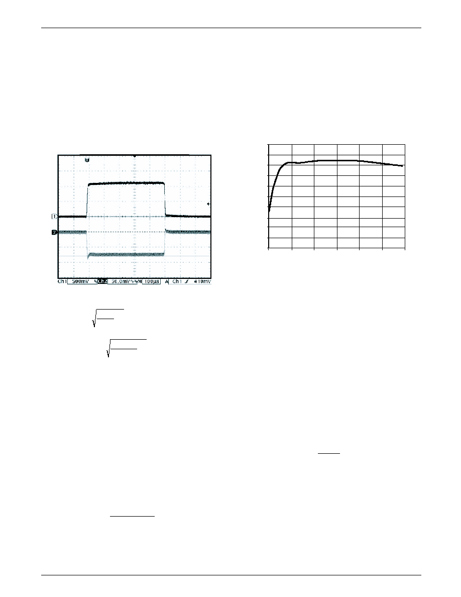
PRODUCT SPECIFICATION
FAN5018B
REV. 1.0.0 Jul/15/05
25
Choosing the closest standard values for these components
yields: C
A
= 390pF, R
A
= 16.9k
, C
B
= 1.5nF, and C
FB
=
33pF.
C
IN
Selection and Input Current di/dt Reduction
In continuous inductor-current mode, the source current of
the high-side MOSFET is approximately a square wave with
a duty ratio equal to n (V
OUT
/V
IN
) and an amplitude of one-
nth of the maximum output current. To prevent large voltage
transients, use a low ESR input capacitor sized for the maxi-
mum rms current. The maximum rms capacitor current is
given by:
Figure 6. Typical Transient Response for Design Example
Note that the capacitor manufacturer's ripple current ratings
are often based on only 2000 hours of life. This makes it
advisable to further derate the capacitor, or to choose a
capacitor rated at a higher temperature than required. Several
capacitors may be placed in parallel to meet size or height
requirements in the design. In this example, the input
capacitor bank is formed by three 2200µF, 16V Nichicon
capacitors with a ripple current rating of 3.5A each.
To reduce the input-current di/dt to below the recommended
maximum of 0.1A/µs, insert an additional small inductor (L
> 1µH @ 15A) between the converter and the supply bus.
That inductor also acts as a filter between the converter and
the primary power source.
Tuning Procedure for the FAN5018B
DC Load Line Setting
1. Build a circuit based on compensation values computed
from the design spreadsheet.
2. Hook up DC load to circuit, turn on and verify opera-
tion. Also check for jitter at no-load and full-load.
3. Measure output voltage at no-load (V
NL
). Verify it is
within tolerance.
Figure 7. Efficiency vs. Output Current
(Circuit of Figure 5)
4. Measure output voltage at full-load cold (V
FLCOLD
).
Let board soak for ~10 minutes at full-load and measure
output (V
FLHOT
). If there is a change of more than a
couple of millivolts, adjust R
CS1
and R
CS2
using
Equations 35 and 37.
5. Repeat Step 4 until cold and hot voltage measurements
remain the same.
6. Measure output voltage from no-load to full-load using
5 Amp steps. Compute the loadline slope for each
change and then average to get overall loadline slope
(R
OMEAS
).
7. If R
OMEAS
is off from R
O
by more than 0.05 m
,
use the following to adjust the R
PH
values:
8. Repeat Steps 6 and 7 to check loadline and repeat
adjustments if necessary.
9. Once the DC loadline adjustment is completed, do not
change R
PH
, R
CS1
, R
CS2
, or R
TH
for the rest of proce-
dure.
1
1
-
◊
◊
◊
=
D
n
I
D
I
O
CRMS
(34)
A
A
I
CRMS
5
.
10
1
125
.
0
3
1
65
125
.
0
=
-
◊
◊
◊
=
(
)
(
)
FLHOT
NL
FLCOLD
NL
OLD
CS
NEW
CS
V
V
V
V
R
R
-
-
◊
=
)
(
2
)
(
2
(35)
80
100
60
40
20
0
20
0
40
OUTPUT CURRENT (A)
EFFICIENCY (%)
60
10
30
50
O
OMEAS
OLD
PH
NEW
PH
R
R
R
R
◊
=
)
(
)
(
(36)
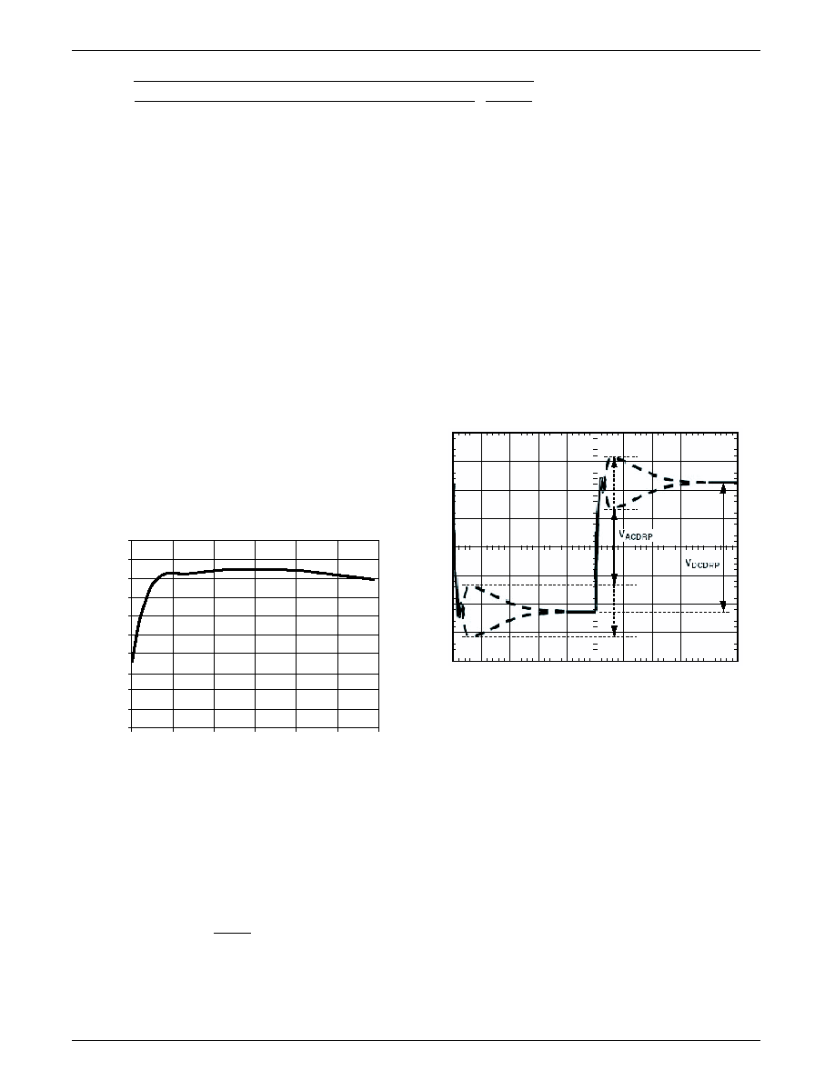
FAN5018B
PRODUCT SPECIFICATION
26
REV. 1.0.0 Jul/15/05
(37)
(
)
(
)
)
25
(
)
25
(
)
(
1
)
(
2
)
(
2
)
25
(
)
(
1
)
25
(
)
(
)
(
1
1
C
TH
C
TH
OLD
CS
NEW
CS
OLD
CS
C
TH
OLD
CS
C
TH
OLD
CS
NEW
CS
o
o
o
o
R
R
R
R
R
R
R
R
R
R
-
-
◊
-
+
◊
+
=
10. Measure the output ripple at no-load and full-load with a
scope and make sure it is within spec.
AC Loadline Setting
11. Remove DC load from circuit and hook up dynamic
load.
12. Hook up scope to output voltage and set to DC coupling
with a time scale at 100µs/div.
13. Set dynamic load for a transient step of approximately
40A at 1kHz with 50% duty cycle.
14. Measure the output waveform (may have to use DC off-
set on scope to see waveform). Try to use a vertical
scale of 100 mV/div or finer.
15. You will see a waveform that looks something like
Figure 8. Use the horizontal cursors to measure V
ACDRP
and V
DCDRP
as shown.
NOTE: DO NOT MEASURE THE UNDERSHOOT OR
OVERSHOOT THAT HAPPENS IMMEDIATELY AFTER
THE STEP.
Figure 8. AC Loadline Waveform
16. If the V
ACDRP
and V
DCDRP
are different by more than a
couple of millivolts, use Equation 38 to adjust C
CS
. You
may need to parallel different values to get the right one
since there are limited standard capacitor values avail-
able (it is a good idea to have locations for two capaci-
tors in the layout for this).
17. Repeat Steps 11 to 13 and repeat adjustments if
necessary. Once complete, do not change C
CS
for the
rest of the procedure.
18. Set the dynamic load step to the maximum step size (do
not use a step size larger than needed) and verify that the
output waveform is square (which means VACDRP and
VDCDRP are equal). NOTE: MAKE SURE LOAD
STEP SLEW RATE AND TURN-ON ARE SET FOR A
SLEW RATE OF ~150≠250A/µs (for example, a load
step of 50A should take 200ns≠300ns) WITH NO
OVERSHOOT. Some dynamic loads will have an
excessive turn-on overshoot if a minimum current is not
set properly (this is an issue if using a VTT tool).
Initial Transient Setting
19. With dynamic load still set at maximum step size,
expand the scope time scale to see 2µs/div to 5µs/div.
You will see a waveform that may have two overshoots
and one minor undershoot (see Figure 9). Here, V
DROOP
is the final desired value.
Figure 9. Transient Setting Waveform
20. If both overshoots are larger than desired, try making
the following adjustments in this order. (NOTE: If these
adjustments do not change the response, you are limited
by the output decoupling.) Check the output response
each time you make a change as well as the switching
nodes (to make sure it is still stable).
a. Make ramp resistor larger by 25% (R
RAMP
).
b. For V
TRAN1
, increase CB or increase switching fre-
quency.
c. For V
TRAN2
, increase R
A
and decrease C
A
by 25%.
21. For load release (see Figure 10), if V
TRANREL
is larger
than V
TRAN1
(see Figure 9), you do not have enough
output capacitance. You will either need more capaci-
tance or need to make the inductor values smaller (if
you change inductors, you need to start the design over
using the spreadsheet and this tuning procedure).
80
100
60
40
20
0
20
0
40
OUTPUT CURRENT (A)
EFFICIENCY (%)
60
10
30
50
DCDRP
ACDRP
OLD
CS
NEW
CS
V
V
C
C
◊
=
)
(
)
(
(38)
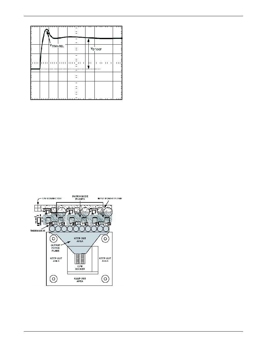
PRODUCT SPECIFICATION
FAN5018B
REV. 1.0.0 Jul/15/05
27
Figure 10. Transient Setting Waveform
Since the FAN5018B turns off all of the phases (switches
inductors to ground), there is no ripple voltage present
during load release. Thus, you do not have to add headroom
for ripple, allowing your load release V
TRANREL
to be larger
than V
TRAN1
by that amount and still be meeting spec. If
V
TRAN1
and V
TRANREL
are less than the desired final droop,
this implies that capacitors can be removed. When removing
capacitors, check the output ripple voltage as well to ensure
it is still within spec.
Layout and Component Placement
The following guidelines are recommended for optimal
performance of a switching regulator in a PC system.
Key layout issues are illustrated in Figure 11.
Figure 11. Layout Recommendations
General Recommendations
∑ For good results, at least a four-layer PCB is
recommended. This should allow the needed versatility
for control circuitry interconnections with optimal
placement, power planes for ground, input, and output
power, and wide interconnection traces in the rest of the
power delivery current paths. Keep in mind that each
square unit of 1 ounce copper trace has a resistance of
~0.53 m
at room temperature.
∑ Whenever high currents must be routed between PCB
layers, vias should be used liberally to create several
parallel current paths so that the resistance and inductance
introduced by these current paths is minimized and the via
current rating is not exceeded.
∑ If critical signal lines (including the output voltage sense
lines of the FAN5018B) must cross through power
circuitry, it is best if a signal ground plane can be
interposed between those signal lines and the traces of the
power circuitry to serves as a shield to minimize noise
injection into the signals..
∑ Use an analog ground plane both around and under the
FAN5018B for ground connections to the components
associated with the controller. Tie this plane to the nearest
output decoupling capacitor ground and not to any other
power circuitry to prevent power currents from flowing in
it.
∑ Connect the components around the FAN5018B close to
the controller with short traces. The most important traces
to keep short and away from other traces are the FB and
CSSUM pins.
∑ Connect the output capacitors as close as possible to the
load (or connector) that receives the power (e.g., a
microprocessor core). If the load is distributed, the
capacitors should also be distributed, and generally in
proportion to where the load tends to be more dynamic.
Power Circuitry
∑ Route the switching power path on the PCB to encompass
the shortest possible length in order to minimize radiated
switching noise energy (i.e., EMI) and conduction losses
in the board. Failure to take proper precautions often
results in EMI problems for the entire PC system as well
as noise related operational problems in the power
converter control circuitry. The switching power path is
the loop formed by the current path through the input
capacitors and the power MOSFETs including all
interconnecting PCB traces and planes. The use of short
and wide interconnection traces is especially critical in
this path for two reasons: it minimizes the inductance in
the switching loop, which can cause high-energy ringing,
and it accommodates the high current demand with
minimal voltage loss. Avoid crossing any signal lines over
the switching power path loop, described below.

FAN5018B
PRODUCT SPECIFICATION
28
REV. 1.0.0 Jul/15/05
∑ Whenever a power dissipating component (e.g., a power
MOSFET) is soldered to a PCB, the liberal use of vias,
both directly on the mounting pad and immediately
surrounding it, is recommended. Two important reasons
for this are: improved current rating through the vias, and
improved thermal performance from vias extended to the
opposite side of the PCB where a plane can more readily
transfer the heat to the air. To achieve the best thermal
dissipation to the air around the board, make a mirror
image of any pad being used to heatsink the MOSFETs on
the opposite side of the PCB . To further improve thermal
performance, use the largest possible pad area.
∑ Route the output power path to encompass a short
distance. The output power path is formed by the current
path through the inductor, the output capacitors, and the
load.
∑ For best EMI containment, use a solid power ground
plane as one of the inner layers extending fully under all
the power components.
Signal Circuitry
∑ The output voltage is sensed and regulated between the
FB pin and the FBRTN pin (which connects to the signal
ground at the load). To avoid differential mode noise
pickup in the sensed signal, the loop area should be small.
Thus the FB and FBRTN traces should be routed adjacent
to each other atop the power ground plane back to the
controller.
∑ Connect the feedback traces from the switch nodes as
close as possible to the inductor. Connect the CSREF
signal to the output voltage at the nearest inductor to the
controller.
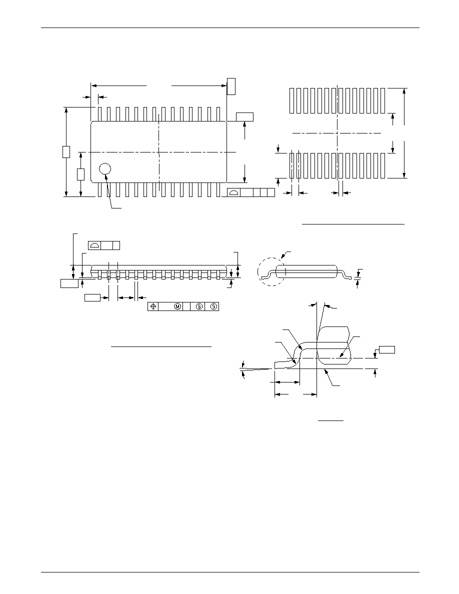
PRODUCT SPECIFICATION
FAN5018B
REV. 1.0.0 Jul/15/05
29
Mechanical Dimensions
28-Pin TSSOP
9.7
± 0.1
15
≠ B ≠
0.1 C
PIN # 1 IDENT
14
ALL Lead Tips
0.2
LAND PATTERN RECOMMENDATION
0.65
0.42
B A
≠ A ≠
4.4
±
0.1
1.78
4.16
7.72
0.51 TYP
28
3.2
6.4
1.2 MAX
ALL LEAD TIPS
0.65
0.19≠0.30
0.13
0.90
See Detail A
0.09≠0.20
0.10
± 0.05
0
∞≠8∞
R0.31
R0.16
.025
GAGE PLANE
SEATING PLANE
DETAIL A
0.61
± 0.1
DIMENSIONS ARE IN MILLIMETERS
NOTES:
A. Conforms to JEDEC registration MO-153, variation AB,
Ref. Note 6, dated 7/93.
B. Dimensions are in millimeters.
C. Dimensions are exclusive of burrs, mold flash, and tie bar extensions.
D Dimensions and Tolerances per ANsI Y14.5M, 1982
1.00
12.00
∞ Top & Botom
+0.15
≠0.10
B
C
A
≠ C ≠

FAN5018B
PRODUCT SPECIFICATION
Jul/15/05 0.0m 005
Stock#DS30005019
© 2003 Fairchild Semiconductor Corporation
LIFE SUPPORT POLICY
FAIRCHILD'S PRODUCTS ARE NOT AUTHORIZED FOR USE AS CRITICAL COMPONENTS IN LIFE SUPPORT DEVICES
OR SYSTEMS WITHOUT THE EXPRESS WRITTEN APPROVAL OF THE PRESIDENT OF FAIRCHILD SEMICONDUCTOR
CORPORATION. As used herein:
1. Life support devices or systems are devices or systems
which, (a) are intended for surgical implant into the body,
or (b) support or sustain life, and (c) whose failure to
perform when properly used in accordance with
instructions for use provided in the labeling, can be
reasonably expected to result in a significant injury of the
user.
2. A critical component in any component of a life support
device or system whose failure to perform can be
reasonably expected to cause the failure of the life support
device or system, or to affect its safety or effectiveness.
www.fairchildsemi.com
DISCLAIMER
FAIRCHILD SEMICONDUCTOR RESERVES THE RIGHT TO MAKE CHANGES WITHOUT FURTHER NOTICE TO
ANY PRODUCTS HEREIN TO IMPROVE RELIABILITY, FUNCTION OR DESIGN. FAIRCHILD DOES NOT ASSUME
ANY LIABILITY ARISING OUT OF THE APPLICATION OR USE OF ANY PRODUCT OR CIRCUIT DESCRIBED HEREIN;
NEITHER DOES IT CONVEY ANY LICENSE UNDER ITS PATENT RIGHTS, NOR THE RIGHTS OF OTHERS.
Ordering Information
Part Number
Temperature Range
Pb Free
Package
Packing
FAN5018BMTCX
0∞C to +85∞C
Yes
TSSOP-28
Tape and Reel