 | –≠–ª–µ–∫—Ç—Ä–æ–Ω–Ω—ã–π –∫–æ–º–ø–æ–Ω–µ–Ω—Ç: FAN5069 | –°–∫–∞—á–∞—Ç—å:  PDF PDF  ZIP ZIP |
FAN5069 Rev. 1.1.0
1
www.fairchildsemi.com
October 2005
©2005 Fairchild Semiconductor Corporation
F
AN5069 PWM and LDO
Contr
o
ller Combo
FAN5069
PWM and LDO Controller Combo
Features
General Purpose PWM Regulator and LDO Controller
Input Voltage Range: 3V to 24V
Output Voltage Range: 0.8V to 15V
VCC
- 5V
- Shunt Regulator for 12V Operation
Support for Ceramic Cap on PWM Output
Programmable Current Limit for PWM Output
Programmable Switching Frequency (200KHz to 600KHz)
R
DS(ON)
Current Sensing
Internal Synchronous Boot Diode
Soft-Start for both PWM and LDO
Multi-Fault Protection with Optional Auto-restart
16-pin TSSOP Package
Applications
PC/Server Motherboard Peripherals
- VCC_MCH (1.5V), VDDQ (1.5V) and VTT_GTL(1.25V)
Power Supply for
- FPGA, DSP, Embedded Controllers, Graphic Card Proces-
sor, and Communication Processors
Industrial Power Supplies
High Power DC-to-DC Converters
Description
The FAN5069 combines a high efficiency PWM controller and a
LDO (Low DropOut) linear regulator controller. Synchronous
rectification provides high efficiency over a wide range of load
currents. Efficiency is further enhanced by using the low-side
MOSFET's R
DS(ON)
to sense current.
Both the linear and PWM regulator soft-start are controlled by a
single external capacitor, to limit in rush current from the supply
when the regulators are first enabled. Current limit for PWM is
also programmable.
The PWM regulator employs a Summing-Current-Mode control
with external compensation to achieve fast load transient
response and provide system design optimization.
FAN5069 is offered in both industrial temperature grade (-40∞C
to +85∞C) as well as commercial temperature grade (-10∞C to
+85∞C)
Ordering Information
Note: Contact Fairchild Sales for availability of other package options.
Part Number Operating Temp. Range Pb-Free
Package
Packing Method
Qty/Reel
FAN5069MTCX
-10∞C to +85∞C
Yes
16-Lead TSSOP
Tape and Reel
2500
FAN5069EMTCX
-40∞C to +85∞C
Yes
16-Lead TSSOP
Tape and Reel
2500

2
www.fairchildsemi.com
FAN5069 Rev. 1.1.0
F
AN5069 PWM and LDO
Contr
o
ller Combo
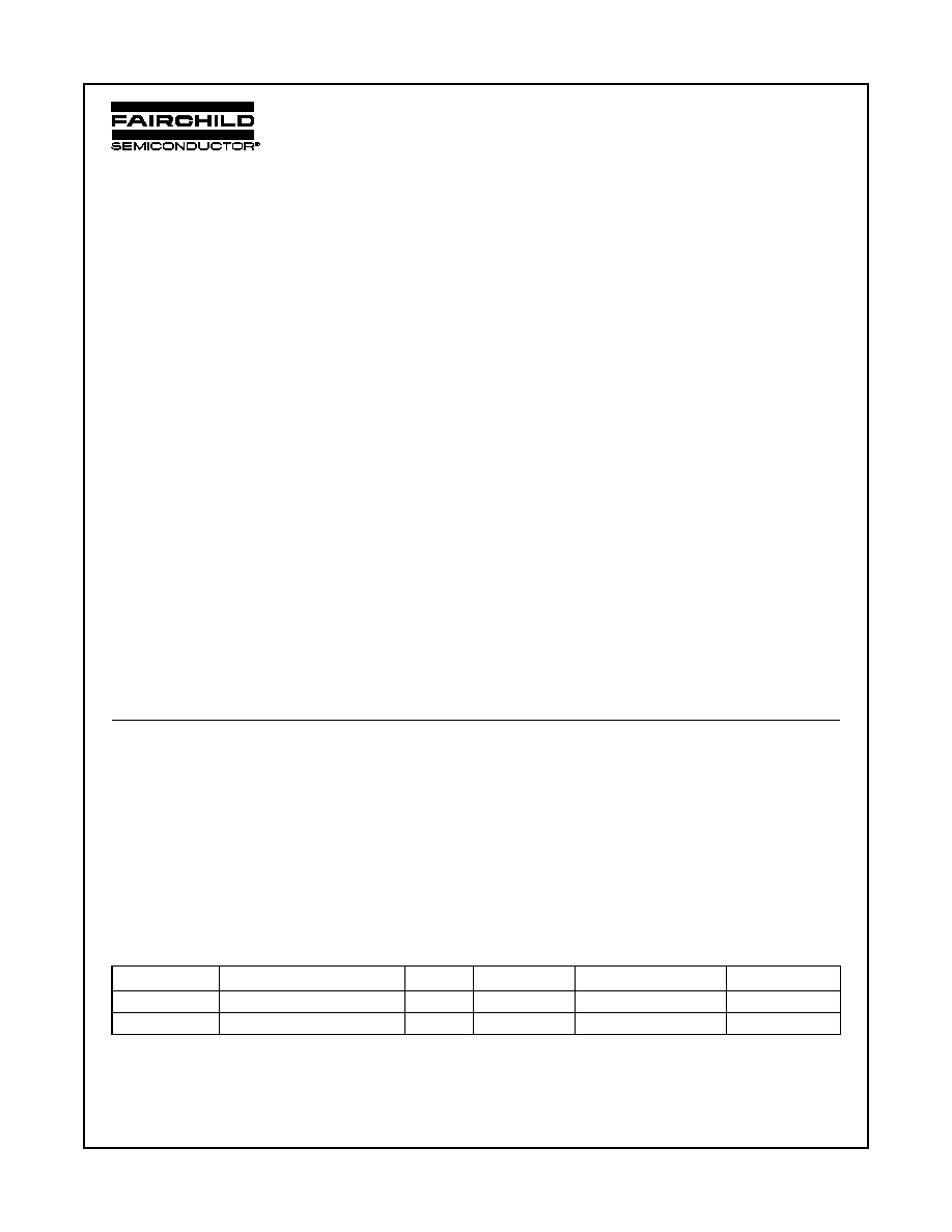
Typical Application
Figure 1. Typical Application Diagram
FAN5069
ILIM
SS
R4
4
3
C3
R(T)
2
EN
7
AGND
8
R5
FB
PWM OUT
Q2
PGND
LDRV
SW
HDRV
BOOT
12
13
9
10
11
6
Q1
COMP
5
R3
3 TO 24V
C2
R1
R2
C6
C7
C4
C1
L1
C5
FBLDO
R7
GLDO
PWM OUT
16
1
LDO OUT
R6
Q3
C8
ULDO
CONTROL
PWM
14
R(RAMP)
VCC
+12V
15
C9
R
VCC
+5V
R8

3
www.fairchildsemi.com
FAN5069 Rev. 1.1.0
F
AN5069 PWM and LDO
Contr
o
ller Combo
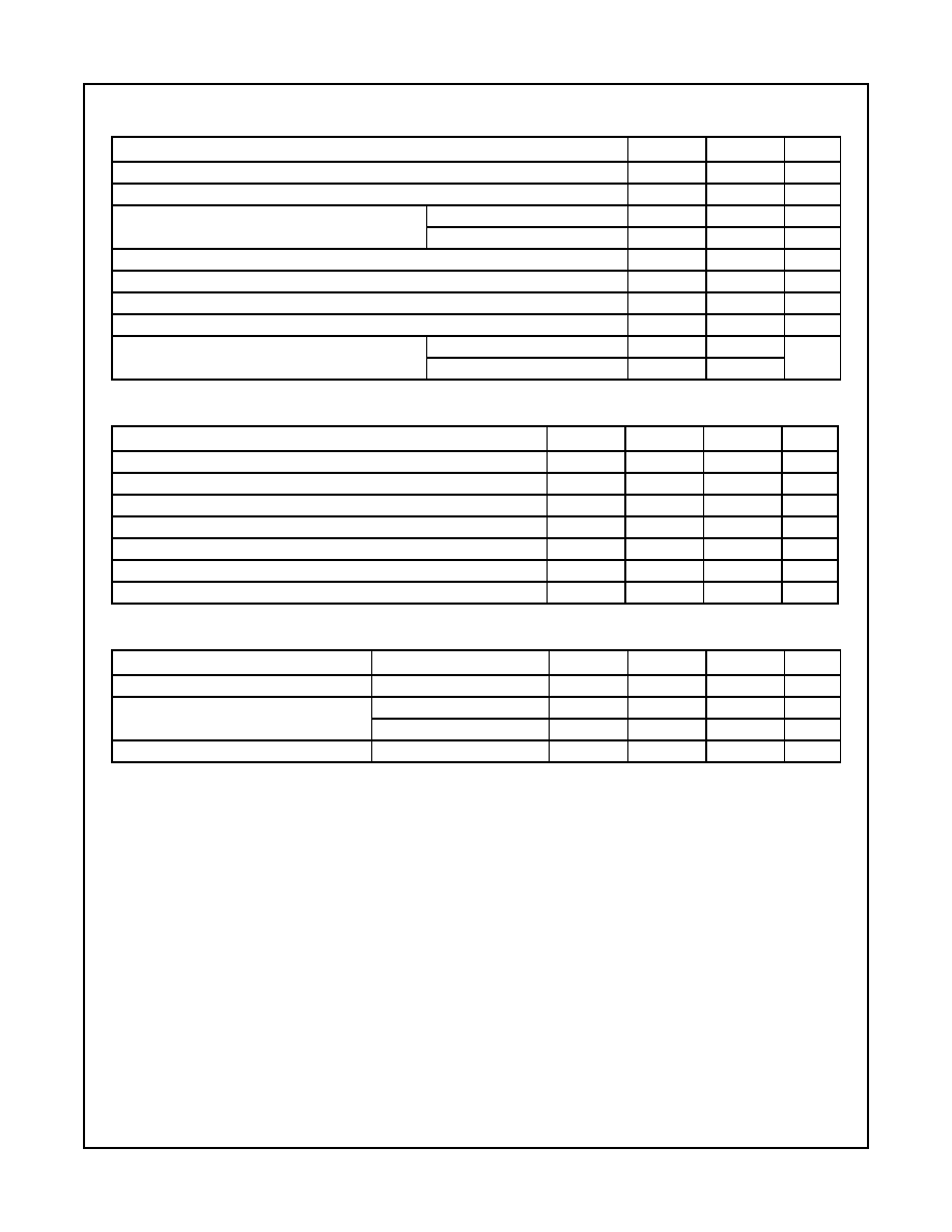
Pin Assignment
Figure 2. Pin Assignment
Pin Description
Pin No.
Pin Name
Pin Description
1
FBLDO
LDO Feedback. This node is regulated to V
REF
.
2
R(T)
Oscillator Set Resistor. This pin provides oscillator switching frequency adjustment. By placing
a resistor (RT) from this pin to GND, the nominal 200kHz switching frequency is increased.
3
ILIM
Current Limit. A resistor from this pin to GND sets the current limit.
4 SS
Soft-Start. A capacitor from this pin to GND programs the slew rate of the converter and the LDO
during initialization. It also sets the time by which the converter will delay when restarting after a
fault occurs. SS has to reach 1.2V before fault shut-down feature is enabled. The LDO is enabled
when SS reaches 2.2V.
5
COMP
COMP. The output of the error amplifier drives this pin.
6
FB
Feedback. This pin is the inverting input of the internal error amplifier. Use this pin, in combina-
tion with the COMP pin, to compensate the feedback loop of the converter.
7
EN
Enable. Enables operation when pulled to logic high. Toggling EN will also reset the regulator
after a latched fault condition. This is a CMOS input whose state is indeterminate if left open and
hence needs to be properly biased at all times.
8
AGND
Analog Ground. The signal ground for the IC. All internal control voltages are referred to this pin.
Tie this pin to the ground island/plane through the lowest impedance connection available.
9
SW
Switching Node. Return for the high-side MOSFET driver and a current sense input. Connect to
source of high-side MOSFET and drain of low-side MOSFET.
10
HDRV
High-Side Gate Drive Output. Connect to the gate of the high-side power MOSFETs. This pin is
also monitored by the adaptive shoot-through protection circuitry to determine when the high-side
MOSFET is turned off.
11
BOOT
Bootstrap Supply Input. Provides a boosted voltage to the high-side MOSFET driver. Connect
to bootstrap capacitor as shown in Figure 1.
12
PGND
Power Ground. The return for the low-side MOSFET driver. Connect to source of low-side MOS-
FET.
13
LDRV
Low-Side Gate Drive Output. Connect to the gate of the low-side power MOSFETs. This pin is
also monitored by the adaptive shoot-through protection circuitry to determine when the lower
MOSFET is turned off.
14
R(RAMP)
Ramp Resistor. A resistor from this pin to VIN sets the ramp amplitude and provides voltage
feed-forward.
15
VCC
VCC. Provides bias power to the IC and the drive voltage for LDRV. Bypass with a ceramic
capacitor as close to this pin as possible. This pin has a shunt regulator which will draw current
when the input voltage is above 5.6V.
16
GLDO
Gate Drive for the LDO. Turned off (low) until SS is greater than 2.2V.
16-Lead TSSOP
Top View
FAN5069
16
15
14
13
12
11
10
9
GLDO
VCC
R(RAMP)
LDRV
PGND
BOOT
HDRV
SW
FBLDO
R(T)
ILIM
SS
COMP
FB
EN
AGND
1
2
3
4
5
6
7
8
4
www.fairchildsemi.com
FAN5069 Rev. 1.1.0
F
AN5069 PWM and LDO
Contr
o
ller Combo
Absolute Maximum Ratings
(Note1)
Thermal Information
Recommended Operating Conditions
Notes:
1. Stresses above those listed under "Absolute Maximum Ratings" may cause permanent damage to the device. This is a stress rating
only and functional operation of the device at these or any other conditions above those indicated in the operational section of this
specification is not implied. Exposure to absolute maximum rating conditions for extended periods may affect device reliability.
Absolute maximum ratings apply individually only, not in combination. Unless otherwise specified all other voltages are referenced
to AGND.
2. Using Mil Std. 883E, method 3015.7(Human Body Model) and EIA/JESD22C101-A (Charge Device Model).
3. Junction to ambient thermal resistance,
JA
, is a strong function of PCB material, board thickness, thickness and number of copper
planes, number of vias used, diameter of vias used, available copper surface, and attached heat sink characteristics.
Parameter
Min.
Max.
Unit
V
CC
to PGND
6
V
BOOT to PGND
33
V
SW to PGND
Continuous
-0.5
33
V
Transient (t < 50nS, F < 500kHz)
-3
33
V
HDRV (V
BOOT
--V
SW
)
6
V
LDRV
-0.5
6
V
All Other Pins
-0.3
V
CC
+0.3
V
Maximum Shunt Current for V
CC
150
mA
Electrostatic Discharge Protection (ESD) Level (Note 2)
HBM
2
kV
CDM
0.4
Parameter
Min.
Typ.
Max.
Unit
Storage Temperature
-65
150
∞C
Lead Soldering Temperature, 10 Seconds
300
∞C
Vapor Phase, 60 Second
215
∞C
Infrared, 15 Seconds
220
∞C
Power Dissipation (P
D
), T
A
= 25∞C
715
mW
Thermal Resistance- Junction to Case(
JC
)
37
∞C/W
Thermal Resistance- Junction to Ambient (
JA
) (Note 3)
100
∞C/W
Parameter
Conditions
Min.
Typ.
Max.
Unit
Supply Voltage (V
CC
)
V
CC
to GND
4.5
5
5.5
V
Ambient Temperature (T
A
)
Commercial
-10
85
∞C
Industrial
-40
85
∞C
Junction Temperature (T
J
)
125
∞C

5
www.fairchildsemi.com
FAN5069 Rev. 1.1.0
F
AN5069 PWM and LDO
Contr
o
ller Combo
Electrical Characteristics
Unless otherwise noted, V
CC
= 5V, T
A
= 25∞C, using circuit in Figure 1.
The `
∑
' denotes that the specifications apply to the full ambient operating temperature range. See Notes 4 and 5.
Symbol
Parameter
Conditions
Min.
Typ.
Max.
Unit
Supply Current
I
VCC
V
CC
Current (Quiescent)
HDRV, LDRV Open
∑
2.6
3.2
3.8
mA
I
VCC(SD)
V
CC
Current (Shutdown)
EN = 0V, V
CC
= 5.5V
∑
200
400
A
I
VCC(OP)
V
CC
Current (Operating)
EN = 5V, V
CC
= 5.0V
10
15
mA
V
SHUNT
V
CC
Voltage (Note 6)
Sinking 20mA to 100mA at V
CC
Pin
5.5
5.9
V
UVLO
UVLO(H)
Rising V
CC
UVLO Threshold
∑
4.0
4.25
4.5
V
UVLO(L)
Falling V
CC
UVLO Threshold
∑
3.6
3.75
4.0
V
V
CC
UVLO Threshold Hystere-
sis
0.5
V
Soft-Start
I
SS
Current
10
A
V
LDOSTART
LDO Start threshold
2.2
V
V
SSOK
PWM Protection Enable
threshold
1.2
V
Oscillator
F
OSC
Frequency
R(T) = 56K
± 1%
240
300
360
KHz
R(T) = Open
160
200
240
KHz
Frequency Range
160
600
KHz
V
RAMP
Ramp Amplitude (Peak-to-
Peak)
R(RAMP) = 330K
0.4
V
Minimum ON Time
F = 200kHz
200
nS.
Reference
V
REF
Reference Voltage (Measured
at FB Pin)
T
A
= 0∞C to 70∞C
∑
790
800
810
mV
T
A
= -40∞C to 85∞C
∑
788
800
812
mV
Current Amplifier Reference
(at SW node)
160
mV
Error Amplifier
DC Gain
80
dB
GBWP
Gain-BW Product
25
MHz
S/R
Slew Rate
10pF across COMP to GND
8
V/
S.
Output Voltage Swing
No Load
∑
0.5
4.0
V
I
FB
FB Pin Source Current
1
A
Gate Drive
R
HUP
HDRV Pull-up Resistor
Sourcing
∑
1.8
3
R
HDN
HDRV Pull-down Resistor
Sinking
∑
1.8
3
R
LUP
LDRV Pull-up Resistor
Sourcing
∑
1.8
3
R
LDN
LDRV Pull-down Resistor
Sinking
∑
1.2
2