 | –≠–ª–µ–∫—Ç—Ä–æ–Ω–Ω—ã–π –∫–æ–º–ø–æ–Ω–µ–Ω—Ç: FAN5078 | –°–∫–∞—á–∞—Ç—å:  PDF PDF  ZIP ZIP |
May 2006
© 2006 Fairchild Semiconductor Corporation
www.fairchildsemi.com
FAN5078 Rev. 1.0.0 ∑ 05/09/06
FAN50
7
8 DDR/ACPI Regulator Combo
FAN5078
DDR/ACPI Regulator Combo
Features
PWM regulator for VDDQ (2.5V or 1.8)
Linear LDO regulator generates VTT = VDDQ/2,
1.5A Peak sink/source capability
AMT / M-state support
Control to generate 5V USB
ACPI drive and control for 5V DUAL generation
3.3V internal LDO for 3V-ALW generation
300 kHz fixed frequency switching
R
DS(ON)
current sensing or optional current sense resistor
for precision over-current detect
Internal synchronous boot diode
Common Power Good signal for all voltages
Input under-voltage lockout (UVLO)
Thermal shutdown
Latched multi-fault protection
Precision reference output for ULDO controllers
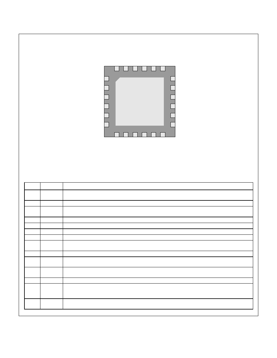
24-pin 5 x 5 MLP package
Applications
DDR VDDQ and VTT voltage generation with ACPI
support
Desktop PC's
Servers
Description
The FAN5078 DDR memory regulator combines a high-
efficiency Pulse-Width Modulated (PWM) controller to
generate the memory supply voltage, VDDQ, and a linear
regulator to generate termination voltage (VTT).
Synchronous rectification provides high efficiency over a wide
range of load currents. Efficiency is further enhanced by using
the low-side MOSFET's R
DS(ON)
to sense current.
The VDDQ PWM regulator is a sampled current mode control
with external compensation to achieve fast load-transient
response and provide system design optimization.
The VTT regulator derives its reference and takes its power
from the VDDQ PWM regulator, output. The VTT termination
regulator is capable of sourcing or sinking 1.5A peak currents.
In S5 M1 mode, the VDDQ switcher, VTT regulator, and the
3.3V regulators remain on. S3 mode keeps these regulators
on, but also turns on an external P-Channel to provide 5V
USB.
A single soft-start capacitor enables controlled slew rates for
both VDDQ and 3.3V-ALW outputs.
PGOOD becomes true in S0 only after all regulators have
achieved stable outputs.
In S5 (EN = 0), the 3.3V internal LDO stays on while the other
regulators are powered down.
Ordering Information
Part Number
Temperature Range
Package
Packing
FAN5078MPX
-10∞C to 85∞C
MLP-24 5x5mm
Tape and Reel
© 2006 Fairchild Semiconductor Corporation
2
www.fairchildsemi.com
FAN5078 Rev. 1.0.0 ∑ 05/11/06
FAN50
78 DDR/ACPI Regulator Combo
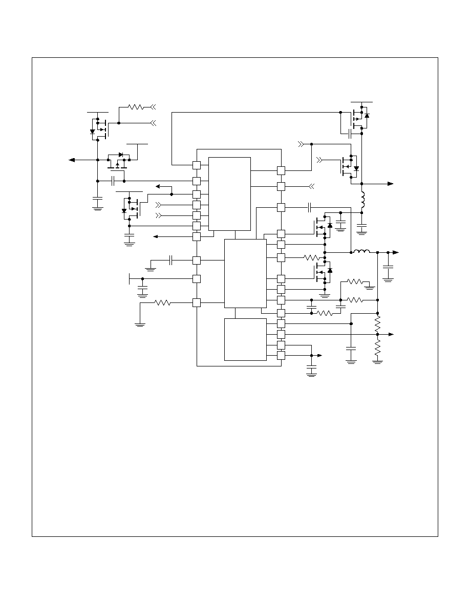
Block Diagrams
FB
ISNS
VCC
+5VSB
VDDQ
R3
L1
Q2
R2
ILIM
VDDQ IN
R1
GND
LDRV
SW
HDRV
BOOT
R5
14
P1
12
10
9
8
11
23
7
20
C2
C4
C5
REF IN
24
5
6
5V MAIN
PGOOD
13
VTT
LDO
3
Q1
COMP
22
C9
R6
C6
C
OUT
Q3
5V DUAL
Q4
+5MAIN
4
C13
16
S3#O
3.3 MAIN
SS
21
C3
S4ST#
2
C12
15
3.3 ALW
S3#I
17
EN
18
PWM
+5VSB
S3#O
Q5
SBSW
1
SBUSB#
Q7
Q6
+5VSB
C14
ACPI
CONTROL
&
LOGIC
S3#O
+5MAIN
C15
+12V
R4
5V USB
R10
C7
VTT SNS
VTT OUT
C8
R9
L2
C
IN
Figure 1. Typical DDR/ACPI System Regulation Schematic
Components are selected for a 15A VDDQ output.
© 2006 Fairchild Semiconductor Corporation
3
www.fairchildsemi.com
FAN5078 Rev. 1.0.0 ∑ 05/11/06
FAN50
78 DDR/ACPI Regulator Combo
Table 1. BOM for Figure 1
Ref.
Qty Description
Mfg. and Part Number
Q1
1
NFET, 30V, 50A, 9m
, DPAK
Fairchild FDD6296
Q2
1
NFET, 30V, 85A, 5m
, DPAK
Fairchild FDD8896
Q3
1
NFET, 30V, 58A, 11m
, DPAK
Fairchild FDD8880
Q4, Q6
2
PFET, 20V, 5.5A, 30m
, SSOT6
Fairchild FDC602P
Q5
1
NFET, 20V, 6.2A, 20m
, SSOT6
Fairchild FDC637AN
Q7
1
NFET, 30V, 30A, 22m
, DPAK
Fairchild FDD6612A
C12,C15
2
330uf, 10V, 20%, 110m
C13
1
10nf, 50V, 10%, X7R
C14
1
3.3nf, 50V, 10%, X7R
C2
1
4.7uf, 25V, 20%, X5R
C4, C8
2
1.0uf, 10V, 10%, X5R
C3, C5
2
0.1uf, 16V, 10%, X7R
C6
1
4.7nf, 50V, 10%, X7R
C7
1
820uf, 6.3V, 20%, 36m
C9
1
82pf, 50V, 5%, NPO
CIN
4
1200uf, 6.3V, 20%, 18m
COUT
3
1200uf, 6.3V, 20%, 18m
L1
1
IND, 1.8uH, 16A, 3.2m
Inter-Technical SC5018-1R8M
L2
1
IND, 470nH, 16A, 2.6m
Inter-Technical SC2511-R47M
R1,R2,R3,R9,R10
5
1.21K, 1%
R4
1
3.9K, 5%
R5
1
71.5K, 1%
R6
1
15.0K, 1%
Contact a Fairchild representative for complete reference design and / or evaluation board.
Bypass Capacitor Notes:
1. Input capacitor C
IN
is typically chosen based on the ripple current requirements. C
OUT
is typically selected based on both
current ripple rating and ESR requirement. See AN-6006 for these calculations.
2. C7, C12, and C15 selection is largely determined by ESR and load transient response requirements. In each case, the
number of capacitors required depends on the capacitor technology chosen. Oscons can meet the requirements with less
space, but higher cost, than using low-ESR electrolytics.
© 2006 Fairchild Semiconductor Corporation
4
www.fairchildsemi.com
FAN5078 Rev. 1.0.0 ∑ 05/11/06
FAN50
78 DDR/ACPI Regulator Combo
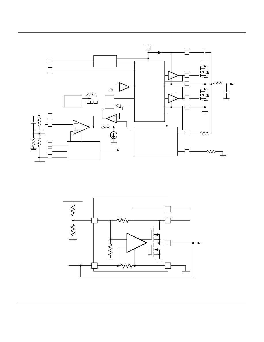
VDDQ IN
S3#I
PGOOD
EN
SS
C
BOOT
Q1
Q2
5VSB
VDD
ADAPTIVE
GATE
CONTROL LOGIC
CURRENT PROCESSING
HDRV
SW
LDRV
PGND
BOOT
ISNS
VIN
C
OUT
VDDQ
PWM
S/H
ILIM
R
ILIM
R
SENSE
ILIM det.
PWM
S
R
Q
RAMP
RAMP
CLK
OVP
POR/UVLO
Reference and
Soft Start
S3
L
OUT
VREF
D2
4.41K
FB
COMP
ISNS
FB
OSC
VCC
VDDQ
Figure 2. PWM Modulator Block Diagram
VTT SNS
VTT OUT
≠
+
EN
S3#I
VDDQ IN
PGND
REF IN
VDDQ IN
50K
50K
110K
R10
R9
Figure 3. VTT Regulator Block Diagram
© 2006 Fairchild Semiconductor Corporation
5
www.fairchildsemi.com
FAN5078 Rev. 1.0.0 ∑ 05/11/06
FAN50
78 DDR/ACPI Regulator Combo
Pin Configuration
SBUSB#
S4ST#
SBSW
5V MAIN
VTT SNS
VTT OUT
P1 = GND
1
2
3
4
5
6
7
8
9
10
11
12
18
17
16
15
14
13
24
23
22
21
20
19
EN
S3#I
S3#O
3.3 ALW
VCC
PGOOD
V
D
D
Q
IN
B
OOT
H
DRV
SW
IS
N
S
L
DRV
RE
F
I
N
FB
COM
P
SS
IL
I
M
GND
FAN5078MP 5x5mm MLP package (
JA
= 38∞C/W)
Note: Connect P1 pad to GND.
Pin Definitions
Pin # Pin
Pin Function Description
1 SBUSB#
USB Standby.
Pulls low with constant current to limit slew rate in S3 if S4ST# is high. Drives a P-
Channel MOSFET to connect 5VSB to 5V USB.
2 S4ST#
S4_STATE#
Connect to system logic signal that enables 5V USB power in S3.
3 SBSW
Standby Switch.
Drives the P-Channel MOSFET to power 5V DUAL from 5VSB when in S3. High in
S0 and S5.
4 5V
MAIN
5V MAIN.
When this pin is below 4.5V, transition from S3 to S0 is inhibited.
5 VTT
SNS
VTT
remote sense input.
6 VTT
OUT
VTT
regulator power output.
7 VDDQ
IN
VDDQ Input
from PWM. Connect to VDDQ output voltage. This is the VTT Regulator power input.
8 BOOT
Boot.
Positive supply for the upper MOSFET driver. Connect as shown in Figure 1. IC contains a boot
diode to VCC.
9 HDRV
High-Side Drive.
High-side (upper) MOSFET driver output. Connect to gate of high-side MOSFET.
10 SW
Switching Node.
Return for the high-side MOSFET driver and a current sense input. Connect to
source of high-side MOSFET and low-side MOSFET drain.
11 ISNS
Current Sense Input.
Monitors the voltage drop across the lower MOSFET or external sense resistor
for current feedback and current limiting.
12 LDRV
Low-Side Drive
The low-side (lower) MOSFET driver output. Connect to gate of low-side MOSFET.
13 PGOOD
Power Good Flag.
An open-drain output that pulls LOW when FB is outside of a ±10% range of the
0.9V reference or the VTT output is < 80% or > 110% of its reference. PGOOD goes low when the IC
is in the S5 state. The power-good signal from the PWM regulator enables the VTT regulator.
14 VCC
VCC.
Provides IC bias and gate drive power. The IC is held in standby until this pin is above the UVLO
threshold.
© 2006 Fairchild Semiconductor Corporation
6
www.fairchildsemi.com
FAN5078 Rev. 1.0.0 ∑ 05/11/06
FAN50
78 DDR/ACPI Regulator Combo
Pin Definitions
(Continued)
Pin
Pin
Name
Pin Function Description
15
3.3
ALW
3.3V LDO Output.
Internal LDO output. Turned off in S0, on in S5 or S3.
16 S3#O
S3#O Output.
Open drain output which pulls the gate of the N-Channel blocking MOSFETs low in S5
and S3. This pin goes high (open) in S0.
17 S3#I
S3 Input.
When LOW, turns off VTT and turns on the 3.3V regulator. Also causes S3#O to pull low to
turn off blocking switch Q3, as shown in Figure 1. PGOOD is low when S3#I is LOW
.
18 EN
ENABLE
Typically tied to the system logic signal S5#. When this pin is low, the IC is in a low quiescent
current state, all regulators are off and S3#O is low.
19,
P1
GND
GROUND
for the IC is tied to this pin and is also connected to P1.
20 ILIM
Current Limit.
A resistor from this pin to GND sets the current limit.
21 SS
Soft Start.
A capacitor from this pin to GND programs the slew rate of the PWM and all LDOs during
initialization and transitions between states.
22 COMP
COMP
Output of the PWM error amplifier. Connect compensation network between this pin and FB.
23 FB
VDDQ Feedback.
The feedback from PWM output. Used for regulation as well as PGOOD, under-
voltage, and over-voltage protection and monitoring.
24 REF
IN
VTT Reference.
Input that provides the reference for the VTT regulator. A precision internal divider from
VDDQ IN (which can be overridden with external resistors) is provided.
Absolute Maximum Ratings
The Absolute Maximum Ratings are those values beyond which the safety of the device cannot be guaranteed. The device
should not be operated at these limits. The parametric values defined in the Electrical Characteristics tables are not guaranteed at
the absolute maximum ratings. The Recommended Operating Conditions table defines the conditions for actual device operation.
Parameter Min.
Max.
Units
VCC
6.5
V
SW, ISNS, HDRV, S3#O,
28
V
BOOT to SW
6.5
V
Continuous -1
20
V
SW, ISNS, HDRV to PGND
Transient (t < 100nS) -5
20
V
All Other Pins
-0.3 -0.3 V
Junction Temperature (TJ )
-20 -20 ∞C
Storage Temperature
-65 -65 ∞C
Lead Soldering Temperature, 10 seconds
∞C
I(VTT) Peak (Duration < 2mS)
-1.5
+1.5
A
I(VTT) RMS
-1.0
+1.0
A
Recommended Operating Conditions
Parameter Conditions
Min.
Typ.
Max.
Units
Supply Voltage VCC
4.5
5
5.5
V
I(3.3 ALW)
1.25
A
Ambient Temperature (TA
)
-10
85
∞C
© 2006 Fairchild Semiconductor Corporation
7
www.fairchildsemi.com
FAN5078 Rev. 1.0.0 ∑ 05/11/06
FAN50
78 DDR/ACPI Regulator Combo
Electrical Specifications
Recommended operating conditions; component values per Figure 1, unless otherwise noted.
Parameter Conditions
Min.
Typ.
Max.
Units
Power Supplies
VCC Current: S0
LDRV, HDRV Open, FB forced above
regulation point, I(VTT) = 0, EN=1, S3#I=1
15
24
mA
S3
EN=1, S3#I = LOW, I(3.3) < 10mA
15
24
mA
S5
EN=0, I(3.3) = 0
2
4
mA
Rising VCC
4.0
4.2
4.4
V
Falling 3.9
4,1
4.3
V
VCC UVLO Threshold
Hysteresis
0.15
V
Rising 4.3
4.4
4.6
V
Falling 3.9
4.1
4.2
V
5V MAIN UVLO Threshold
Hysteresis
0.30
V
5V MAIN Input Resistance
to GND
35
62
K
Oscillator
Frequency
255
300
345
KHz
Ramp Amplitude, pk≠pk
(1)
1.8 V
Ramp Offset
0.5
V
Reference and Soft Start
Internal Reference Voltage
0.891
0.900
0.909
V
ILIM Reference Voltage
-2
A > I
ILIM
> -18
A
0.882 0.900 0.918 V
Initial ramp after power-up
4.2
Average Soft Start Current
(ISS)
During PWM / LDO soft start
45
µA
SS Discharge Resistance
EN = 0
150
SS Complete Threshold
1.5
V
SS Complete Hysteresis
50
mV
PWM Converter
Load Regulation
IOUT from 0 to 15A
-2
+2
%
FB Bias Current
-1.8
-1.3
-0.8
µA
Under-Voltage Shutdown
as % of set point, 2
S noise filter
65 75 80 %
Over-Voltage Threshold
as % of set point
110
115
120
%
ISNS Over-Current Threshold RILIM= 56K
-195 -170 -145 µA
VDDQ IN Discharge
Resistance
EN = 0
20
55
COMP Source Current
V
COMP
= 2.5V
650
µA
COMP Sink Current
V
COMP
= 2.5V
100
µA
Error Amp GBW Product
(1)
5.5 MHz
Error Amp DC Gain
(1)
82
dB
© 2006 Fairchild Semiconductor Corporation
8
www.fairchildsemi.com
FAN5078 Rev. 1.0.0 ∑ 05/11/06
FAN50
78 DDR/ACPI Regulator Combo
Electrical Specifications
(Continued)
Parameter Conditions
Min.
Typ.
Max.
Units
PWM Output Driver
Sourcing
1.8
3
HDRV Output Resistance
Sinking
1.8
3
Sourcing
1.8
3
LDRV Output Resistance
Sinking
1.2
2
PGOOD output
Lower Threshold
as % of set point, 2
S noise filter
86 92
%
Upper Threshold
as % of set point, 2
S noise filter
108 115
%
PGOOD Output Low
IPGOOD = 1.5 mA
0.5
V
Leakage Current
VPULLUP = 5V
1
µA
3.3V LDO
Regulation
I(3.3) from 0-1.25A, VCC > 4.75V
3.2
3.3
3.4
V
VTT Regulator
VDDQ IN Current
S0 mode, I
VTT
=0
35
70
mA
VREF IN to VTT
Differential Output Voltage
I
VTT
= 0, T
A
=25∞C
I
VTT
=
± 1.25A (pulsed)
-20
-40
20
40
mV
VTT Current Limit
Pulsed (300mS max.)
(1)
±1.5
±3
±4
A
VTT Leakage Current
EN = LOW
-20
20
µA
VTT SNS Input Resistance
VTT SNS to GND
110
K
VTT PGOOD Threshold
Measured at VTT SNS
80
110
% VTT
REF
Drop-Out Voltage
I
VTT
=
± 1.5A
-0.8 0.8 V
Control Functions
EN, S4ST# Input Threshold
1.0
1.25
1.55
V
S3#I Input Threshold
1.3
1.5
1.7
V
S3#I, EN, S4ST# Input Current
-1
1
µA
Over-Temperature
Shutdown
150 ∞C
Over-Temperature Hysteresis
25
∞C
S3#O Output Low R
DS(ON)
170
300
S3#O Output High Leakage
V(S3#O) = 12V
1
5
µA
SBSW Pull-down Resistance
5V MAIN OK
150
200
SBSW Pull-up Resistance
900
1200
SBUSB# Pull-down
Resistance
5V MAIN OK
150
200
SBUSB# pull-up resistance
550
750
SBSW, SBUSB# Output
Current
5V MAIN < UVLO
500
nA
Notes:
1. Guaranteed by design and characterization, not tested in production.
© 2006 Fairchild Semiconductor Corporation
9
www.fairchildsemi.com
FAN5078 Rev. 1.0.0 ∑ 05/11/06
FAN50
78 DDR/ACPI Regulator Combo
Circuit Description
Overview
The FAN5078 provides five functions:
1. A general purpose PWM regulator, typically used to
generate VDDQ for DDR Memory.
2. A low-dropout linear VTT regulator capable of sinking
and sourcing 1.5A peak.
3. Control to generate 5V DUAL using an external N-
channel to supply power from 5V MAIN in S0 and an
external P-Channel to provide power from 5V Standby
(5VSB) in S3.
4. Drive to generate 5V USB. This signal drives a P-
Channel MOSFET to connect 5V USB to +5VSB in S3.
5. An internal LDO that regulates 3.3V-ALW in S3 mode
from VCC (5VSB). In S3 or S5, this regulator is capable
of 1.25A peak currents with average currents limited by
the thermal design of the PCB.
At initial power-up, or when transitioning from S5, the PWM
regulator is disabled until 5V MAIN is above its UVLO
threshold.
Table 2. ACPI states
STATE
EN
(S5#) S3#I S4ST# SBSW SBUSB# S3#O VDDQ VTT
3.3 ALW
LDO
3.3 ALW
5V Dual
5V USB
S5
L
X
X
H
H
L
OFF OFF
ON
LDO
OFF
OFF
S5 M1
H
L
L
L
H
L
ON
ON
ON
LDO
+5VSB
OFF
S3
H
L
H
L
L
L
ON
ON
ON
LDO
+5VSB
+5VSB
S0
H
H
X
H
H
H
ON
ON
OFF
3.3V MAIN
+5 MAIN
+5 MAIN
Regulator Sequencing
The VCC pin provides power to all logic and analog control
functions of the regulator, including:
1. Power for the 3.3V regulator
2. LDRV gate driver current
3. HDRV boot diode charging current
4. The regulator analog control and logic.
This pin must be decoupled with a X5R ceramic capacitor
(1
F or larger recommended) as close as possible to the VCC
pin. After VCC is above UVLO, the start-up sequence begins
(see Figure 8).
UVLO on VCC discharges SS and resets the IC.
T0 to T3:
After initial power-up, the IC ignores logic inputs for
a period (T3-T0) of approximately:
SS
C
7
.
1
T0
-
T3
∑
(1)
where T3-T0 is in mS if C
SS
is in nF. At T2 (about 2/3 of the
way from T1 to T3), the 3.3V-ALW LDO is in regulation. The
3.3V LDO's slew rate is limited by the discharge slope of CSS.
If 3.3V MAIN has come up prior to this time, the 3.3V-ALW
node is already pre-charged through the body diode of Q5
(see Figure 1).
T3 to T4:
The IC starts VDDQ only if 5V MAIN is above its
UVLO threshold (5V MAIN OK). Provided 5V MAIN is up
before T3, the IC waits about 100
S before initiating soft-start
on VDDQ to allow CSS time to fully discharge. The IC is in
"SLEEP" or S5 state when EN is low. In S5, only the 3.3V
LDO is on. If the IC is in S5 at T4, CSS is held to 0V.
T4 to T5:
After VDDQ is stabilized (when C
SS
is at about
~1.3V), an internal VDDQ OK is generated that allows the
VTT LDO to start. To ensure that the VDDQ output is not
subjected to large transient currents, the VTT slew rate is
limited by the slew rate of the SS cap. In addition, the VTT
regulator is current limited. VTT is in regulation once C
SS
reaches about 3.8V.
S0 to S3 or S5 M1:
The system signals this transition by
dropping the S3#I signal. When this occurs, S3#O goes low,
and the 3.3V LDO turns on. SBSW pulls low to turn on the P-
Channel 5V DUAL switch. SBUSB# pulls low to turn on Q6
when S4ST# is high.
S3 or S5 M1 to S0:
The system signals this transition by
raising the S3#I signal. S0 mode is not entered until 5V MAIN
OK, then the following occurs:
S3#O releases
SBSW and SBUSB# both pull high to turn off their
P-Channel switches
The 3.3V LDO turns off.
In most systems, the ATX power supply is enabled when S3#I
goes from high. At that time, 5V and 3.3V MAIN starts to rise.
When the FAN5078's 5V MAIN pin is above its UVLO
threshold, Q3 and Q5 turn on. This can cause about a 10%
"dip" in both 5V DUAL and 3.3V ALW when Q3 and Q5 turn
on, since at that point, 5V MAIN and 3.3V MAIN are at 90% of
their regulation value.
© 2006 Fairchild Semiconductor Corporation
10
www.fairchildsemi.com
FAN5078 Rev. 1.0.0 ∑ 05/11/06
FAN50
78 DDR/ACPI Regulator Combo
S3#I
5V MAIN
4.4V
5V DUAL
5V Dual "dip"
S3#O
Figure 4. S3 to S0 Transition: 5V DUAL
This dip can also occur in 5V USB and 3.3V-ALW if 5V and
3.3V are not fully charged before the 5V MAIN pin exceeds its
threshold. To eliminate the dip, add delay to the 5V MAIN pin,
as shown below. The 5V MAIN pin on the FAN5078 does not
supply power to the IC; it is only used to monitor the voltage
level of the 5V MAIN supply. The pin does have a pull-down
resistor impedance of about 62K and therefore requires a low
value RDLY resistor (see Figure 5 below).
5V MAIN
4
+5MAIN
FROM
ATX
R
DLY
C
DLY
Figure 5. Adding Delay to 5V MAIN
Another method to eliminate the potential for this dip is to
instead connect the ATX power supply's PWR_OK signal to
the 5V MAIN pin. Some systems cannot tolerate the long
delay for PWR_OK (>100mS) to assert, hence the solution in
Figure 5 may be preferable.
If the PWR_OK signal is used, the voltage at the 5V MAIN pin
must reach the 5V MAIN threshold. Since the internal pull-
down resistance of the 5V MAIN pin is 62K, a low value pull-
up should be used. A lower current solution can also be used
by employing the 12V supply to provide adequate pull-up
capability. The circuit in Figure 6 requires that PWR_OK, 12V,
and +5MAIN from the ATX are all up before allowing the IC to
go to S0.
5V MAIN
4
PWR_OK
+12V
10K
5VS B
FR
O
M
A
T
X
Figure 6. Using PWR_OK to Enable 5V MAIN
Care should also be taken to ensure that 3.3V-ALW does not
glitch during the transition to S0. As shown in Figure 7, the
3.3V internal regulator turns off as soon as 5V MAIN crosses
its rising threshold, releasing S3#O. While the gate
capacitances of Q5, Q7, and Q3 charge sufficiently to turn Q5
on, the load current on 3.3-ALW is supplied by C12. There is
an initial "ESR step" of I
3.3
x ESR
C12
, where I
3.3
is the 3.3-ALW
load current. This is followed by a discharge of C12 whose
slope is proportional to
12
C
I
3
.
3
. To ensure that the drop in 3.3-
ALW during this transition does not cause system problems,
use sufficiently low ESR capacitors and a sufficiently low value
for R4 to ensure that 3.3-ALW remains inside the required
system tolerance.
S3#I
3.3-ALW
S3#O
(Q5 gate)
5V MAIN
4.4V
ON
3.3V LDO
OFF
I
3.3
x ESR
C12
Figure 7. 3.3V-ALW Transition to S0
S5 to S5 M1 or S3:
During S5 to S3 transition, the IC pulls
SBSW (or SBUSB# if enabled by S4ST#) low with a 500nA
current sink to limit inrush in Q4 if 5V MAIN is below its UVLO
threshold. At that time, 5V DUAL and 5V USB are discharged.
The limited gate drives control the inrush current through Q4
or Q6 as they charge their respective load capacitances on 5V
DUAL and 5V USB respectively. Depending on the C
GD
of Q4
and Q6, the current available from 5VSB, and the size of C
IN
and C15, C13 and C14 may be omitted.
)
4
Q
(
GD
7
)
INRUSH
(
4
Q
C
13
C
10
X
5
CIN
I
+
∑
=
-
)
6
Q
(
GD
7
)
INRUSH
(
6
Q
C
14
C
10
X
5
15
C
I
+
∑
=
-
(2)
If 5V MAIN is above its UVLO threshold, SBSW (or SBUSB# if
enabled by S4ST#) is pulled down with an impedance of
~150. VDDQ and VTT do not start until 5V MAIN OK is true.
© 2006 Fairchild Semiconductor Corporation
11
www.fairchildsemi.com
FAN5078 Rev. 1.0.0 ∑ 05/11/06
FAN50
78 DDR/ACPI Regulator Combo
VDDQ
5V SB
V(UVLO)
4V
1V
3.3V LDO
T0
3.8V
T1
T2
T3 T4 T5
SS
Figure 8. Start-up Sequence into S0
PWM Regulator
A PSPICE model and spreadsheet calculator are available
in Application Note AN-6006 for the VDDQ PWM regulator
to select external components and verify loop stability. The
topics covered below provide the explanation behind the
calculations in the spreadsheet.
Setting the Output Voltage
The output voltage of the PWM regulator can be set in the
range of 0.9V to 80% of its power input by an external
resistor divider.
The internal reference is 0.9V. The output is divided down
by an external voltage divider to the FB pin (for example, R1
and R2 in Figure 1). There is also a 1.3
A current sourced
out of FB to ensure that if the pin is open, VDDQ remains
low. The output voltage therefore is:
A
3
.
1
1
R
V
9
.
0
V
2
R
V
9
.
0
OUT
+
-
=
(3a)
To minimize noise pickup on this node, keep the resistor to
GND (R2) below 2K. In the example below, R2 is 1.82K and
R1 is calculated:
A
3
.
1
9
.
0
)
9
.
0
V
(
2
R
1
R
OUT
-
-
∑
=
=
1.815K
1.82K
(3b)
The synchronous buck converter is optimized for 5V input
operation. The PWM modulator uses an average current
mode control for simplified feedback loop compensation.
Oscillator
The oscillator frequency is 300Khz. The internal PWM ramp
is reset on the rising clock edge.
PWM Soft Start
When the PWM regulator is enabled, the circuit waits until
the VDDQ IN pin is below 100mV to ensure that the soft-
start cycle does not begin with a large residual voltage on
the PWM regulator output.
When the PWM regulator is disabled, 40
is connected
from VDDQ IN to PGND to discharge the output. The circuit
waits until the FB pin is below 100mV to ensure that the
soft-start cycle does not begin with a large residual voltage
on the VDDQ regulator output.
The voltage at the positive input of the error amplifier is
limited to V
CSS,
which is charged with about 45
A. Once C
SS
has charged to 0.9V, the output voltage is in regulation.
© 2006 Fairchild Semiconductor Corporation
12
www.fairchildsemi.com
FAN5078 Rev. 1.0.0 ∑ 05/11/06
FAN50
78 DDR/ACPI Regulator Combo
LDRV
PGND
ISNS
2.5V
ILIM det.
R
SENSE
I2 =
ILIM*9.6
ILIM
0.9V
R
ILIM
ILIM
mirror
in +
in ≠
V to I
ISNS
ISNS
S/H
SS/EN
C
SS
FB
Reference and
Soft Start
TO
PWM
COMP
4.41K
COMP
Figure 10. Current Limit / Summing Circuits
The time it takes SS to reach 0.9V, and VDDQ to achieve
regulation is:
45
C
X
9
.
0
T
SS
0.9
(4)
where T
0.9
is in mS if C
SS
is in nF.
CSS charges another 400mV before the PWM regulator's
fault latch is enabled. When CSS reaches 1.2V, the VTT
regulator begins its soft-start. After VTT is in regulation,
PGOOD is allowed to go HIGH (open).
Reference Output for ULDO Controllers
The FAN5078's ILIM pin (pin 20) may be used as a
precision 0.9V reference for external ULDO controllers, as
shown in Figure 9. The ILIM pin is on during all ACPI states.
Q1
ILIM
R5
20
R3
U1
R1
R2
5VSB
C1
VOUT
COUT
Figure 9. Using ILIM as a ULDO Reference
R5 in Figure 1 is the current limit setting resistor and
comprises the only DC current path from the ILIM pin to
GND. The circuit is configured so that the reference for the
ULDO is presented at the positive terminal of U1 and draws
negligible DC current. R3 and C1 filter noise that might be
induced if there is significant PCB trace length. C1 should
be placed as close as possible to the op-amp's input pin. R3
should be placed as close as possible to pin 20 of the
FAN5078 and should be greater than 10K to isolate the
ILIM pin from noise.
Recommended values for the circuit of Figure 9:
R3 50K
R5 See
AN-6006
C1 1nF
R1, R2
Per desired VOUT:
+
∑
=
2
R
1
R
1
9
.
0
VOUT
© 2006 Fairchild Semiconductor Corporation
13
www.fairchildsemi.com
FAN5078 Rev. 1.0.0 ∑ 05/11/06
FAN50
78 DDR/ACPI Regulator Combo
Current Processing Section
The following discussion refers to Figure 10.
The current through R
SENSE
resistor (ISNS) is sampled
shortly after Q2 is turned on. That current is held and summed
with the output of the error amplifier. This effectively creates a
current mode control loop. R
SENSE
sets the gain in the
current feedback loop. For stable operation, the voltage
induced by the current feedback at the PWM comparator input
should be set to 30% of the ramp amplitude at maximum load
current and line voltage.
Equation 5 estimates the recommended value of R
SENSE
as
a function of the maximum load current ( I
LOAD(MAX)
) and the
value of the MOSFET's R
DS(ON)
:
100
V
125
.
0
%
30
4.41K
R
I
R
IN(MAX)
DS(ON)
)
MAX
(
LOAD
SENSE
-
∑
∑
∑
∑
=
(5)
where R
DS(ON)
is the maximum R
DS(ON)
of the low-side
MOSFET at its maximum temperature.
R
SENSE
must, however, be kept higher than:
100
A
145
R
I
R
DS(ON)
)
MAX
(
LOAD
SENSE(MIN)
-
∑
=
(6)
Setting the Current Limit
ISNS is compared to the current established when a 0.9 V
internal reference drives the ILIM pin. R
ILIM
, the R
DS(ON)
of Q2,
and R
SENSE
determine the current limit:
DS(ON)
SENSE
LIMIT
ILIM
R
)
R
(100
X
I
9.6
R
+
=
(7)
where ILIMIT is the peak inductor current. Since the tolerance
on the current limit is largely dependent on the ratio of the
external resistors it is fairly accurate if the voltage drop on the
switching node side of R
SENSE
is an accurate representation
of the load current. When using the MOSFET as the sensing
element, the variation of R
DS(ON)
causes proportional variation
in the ISNS. This value not only varies from device to device,
but also has a typical junction temperature coefficient of about
0.4% / ∞C (consult the MOSFET datasheet for actual values),
so the actual current limit set point decreases proportional to
increasing MOSFET die temperature. A factor of 1.6 in the
current limit set point should compensate for MOSFET R
DS(ON)
variations, assuming the MOSFET's heat sinking keeps its
operating die temperature below 125∞C.
Current limit (I
LIMIT
) should be set sufficiently high as to allow
the inductor current to rise in response to an output load
transient. Typically, a factor of 1.3 is sufficient. In addition,
since I
LIMIT
is a peak current cut-off value, multiply I
LOAD(MAX)
by the inductor ripple current (i.e. 20%). To account all of
these variations, set ILIMIT as:
ILIMIT > I
LOAD(MAX)
x 1.6 x 1.3 x 1.2
(8)
LDRV
PGND
ISNS
R
SENSE
R1
Q2
Figure 11. Improving Current Sensing Accuracy
More accurate sensing can be achieved by using a resistor
(R1) instead of the R
DS(ON)
of the FET, as shown in Figure
11. This approach causes higher losses, but greater accuracy.
Gate Drive
The adaptive gate control logic translates the internal PWM
control signal into the MOSFET gate drive signals, providing
necessary amplification, level shifting, and shoot-through
protection. It also has functions to help optimize the IC
performance over a wide range of operating conditions.
Since MOSFET switching time can vary dramatically from type
to type and with the input voltage, the gate control logic
provides adaptive dead time by monitoring the gate-to-source
voltages of both upper and lower MOSFETs. The lower
MOSFET drive is not turned on until the gate-to-source
voltage of the upper MOSFET has decreased to less than
approximately 1 volt. Similarly, the upper MOSFET is not
turned on until the gate-to-source voltage of the lower
MOSFET has decreased to less than approximately 1 volt.
This allows a wide variety of upper and lower MOSFETs to
be used without a concern for simultaneous conduction or
shoot-through.
There must be a low-resistance, low-inductance path between
the driver pin and the MOSFET gate for the adaptive dead-
time circuit to work properly. Any delay along that path
subtracts from the delay generated by the adaptive dead-time
circuit and shoot-through may occur.
© 2006 Fairchild Semiconductor Corporation
14
www.fairchildsemi.com
FAN5078 Rev. 1.0.0 ∑ 05/11/06
FAN50
78 DDR/ACPI Regulator Combo
Frequency Loop Compensation
The loop is compensated using a feedback network around
the error amplifier.
R4
VREF
VDDQ
FB
COMP
R3
R2
R1
C3
C1
C2
Figure 12. Compensation Network
Figure 12 shows a complete Type 3 compensation network. A
Type 2 compensation configuration eliminates R4 and C3 and
is shown in Figure 1. Since the FAN5078 architecture employs
summing current mode, Type 2 compensation can be used for
most applications. For critical applications that require wide
loop bandwidth and use very low ESR output capacitors, Type
3 compensation may be required. The PSPICE model and
spreadsheet calculator of AN-6006 can be used to calculate
these component values.
Transient response during a rapid decrease in I
LOAD
can be
improved by adding a pull-down resistor (> 5K) from the
COMP pin to GND.
PGOOD Signal
PGOOD monitors the status of the PWM output as well as
VTT. PGOOD remains low unless all of the conditions below
are met:
SS is above 3.5V
Fault latch is cleared
FB is between 90% and 110% of VREF
VTT is in regulation.
Protection
The converter output is monitored and protected against
extreme overload, short circuit, over-voltage and under-
voltage conditions.
An internal fault latch is set for any fault intended to shut down
the IC. When the fault latch is set, the IC discharges its output
by driving LDRV high until VDDQ IN < 0.5V. LDRV then goes
low until VDDQ IN > 0.8V. This discharges VDDQ without
causing undershoot (negative output voltage).
To discharge the output capacitors, a 40
load resistor is
switched in from VDDQ IN to PGND whenever the IC is in
fault condition or when EN is low. After a latched fault,
operation can be restored by recycling power or toggling the
EN pin.
Under-Voltage Shutdown
If FB stays below the under-voltage threshold for 2
S, the fault
latch is set. This fault is prevented from setting the fault latch
during PWM soft-start (SS < 1.3V).
Over-Current Sensing
If the circuit's current limit signal (ILIM det shown in Figure 10)
is high at the beginning of a clock cycle, a pulse-skipping
circuit is activated and HDRV is inhibited. The circuit continues
to pulse skip in this manner for the next 8 clock cycles. If, at
any time from the 9
th
to the 16
th
clock cycle, the ILIM det is
again reached, the fault latch is set. If ILIM det does not occur
between cycle 9 and 16, normal operation is restored and the
over-current circuit resets itself.
This fault is prevented from setting the fault latch during soft-
start (SS < 1.3V).
Figure 13. Over-Current Protection Waveforms
OVP / HS Fault / FB short to GND detection
A HS Fault is detected when there is more than 0.5V from SW
to PGND 350nS after LDRV reaches 4V (same as the current
sampling time).
OVP fault detection occurs if FB > 115% VREF for 16 clock
cycles.
During soft-start, the output voltage could potentially "run
away" if either the FB pin is shorted to GND or R1 is open.
This fault is detected if the following condition persists for
more than 14
S during soft-start:
VDDQ IN (PWM output voltage) > 1V
FB < 100mV
Any of these faults sets the fault latch, even during the SS
time (SS < 1.2V).
© 2006 Fairchild Semiconductor Corporation
15
www.fairchildsemi.com
FAN5078 Rev. 1.0.0 ∑ 05/11/06
FAN50
78 DDR/ACPI Regulator Combo
To ensure that FB pin open does not cause a destructive
condition, a 1.3
A current source ensures that the FB pin is
high if open. This causes the regulator to keep the output low
and eventually results in an under-voltage fault shutdown
(after PWM SS completes).
4.
4
1
K
ISNS
RAMP
SS
FB
COMP
1.3
A
I
SS
≠
+
+
E/A
VREF
≠
+
+
PWM
Figure 14. SS Clamp and FB Open Protection
Over-Temperature Protection
The chip incorporates an over-temperature protection circuit
that shuts the chip down when a die temperature of about
150∞C is reached. Normal operation is restored when the die
temperature falls below 125∞C with internal Power On Reset
asserted, resulting in a full soft-start cycle. To accomplish this,
the over-temperature comparator discharges the SS pin.
VTT Regulator Section (Figure 3)
The VTT regulator includes an internal resistor divider (50K for
each resistor) from the output of the PWM regulator. If the
REF IN pin is left open, the divider produces a voltage 50% of
VDDQ IN. Using a low impedance external precision voltage
divider produces greater accuracy.
The VTT regulator is enabled when S3#I is HIGH and the
PWM regulator's internal PGOOD signal is true. The VTT
regulator also includes its own PGOOD signal, which is high
when VTT SNS > 90% of REF IN.
FAN5078 Design Tools
AN-6006 provides a PSPICE model and spreadsheet
calculator for the PWM regulator, simplifying external
component selections, and verifying loop stability.
The spreadsheet calculator can be used to calculate all
external component values for the FAN5078. The spreadsheet
calculates compensation components that can be verified in
the PSPICE model to ensure stability.
The PSPICE model in AN-6006 simulates both loop stability
(Bode Plot) and transient analysis, and can be customized
for a wide variety of applications and external component
configurations.
As an initial step, define:
Output voltage
Maximum PWM output load current
Maximum load transient current and maximum allowable
output drop during load transient
R
DS(ON)
of the low-side MOSFET (Q2)
Maximum allowable output ripple.
Power MOSFET Selection
For a complete analysis of MOSFET selection and efficiency
calculations, see Application Note
AN-6005: Synchronous
Buck MOSFET Loss Calculations with Excel Mode
l.
3.3V and VTT LDO Output Capacitors
For stability, use at least 100
F for 3.3V-ALW bypass
capacitor with a minimum ESR of 20m.
The VTT output is typically bypassed with 820
F with at least
30m ESR.
© 2006 Fairchild Semiconductor Corporation
16
www.fairchildsemi.com
FAN5078 Rev. 1.0.0 ∑ 05/11/06
FAN50
78 DDR/ACPI Regulator Combo
Dimensional Outline Drawing
Notes:
1. Conforms to JEDEC registration number MO-220, variation WHHC, dated Aug/2002.
2. Dimensions are in millimeters.
3. Dimensions and tolerances per ASME y14.5-1994.