©2005 Fairchild Semiconductor Corporation
1
www.fairchildsemi.com
May 2005
FAN5182 Rev. 1.0.1
F
AN5182 Adjustab
le Output 1,
2,
or 3-Phase Sync
hr
onous Buc
k Contr
oller
FAN5182
Adjustable Output 1, 2, or 3-Phase Synchronous Buck
Controller
Features
Selectable 1-, 2-, or 3-phase operation at up to 1MHz per
phase
±2% Worst-case differential sensing error over temperature
Externally adjustable 0.8V to 5V output from a 12V supply
Logic-level PWM outputs for interface to external high-power
drivers
Active current balancing between all phases
Built-in power-good/crowbar functions
Programmable over current protection with adjustable latch-
off delay
Applications
Auxiliary supplies
DDR memory supplies
Point-of-load supplies
Description
The FAN5182 is a highly efficient multi-phase synchronous buck
switching regulator controller optimized for converting a 12V
main supply into a high-current low voltage supply for use in
point-of-load (POL) applications. It uses a multi-loop PWM
architecture to drive the logic-level outputs at a programmable
switching frequency that can be optimized for regulator size and
efficiency. The phase relationship of the output signals can be
programmed to provide 1, 2, or 3-phase operation, allowing for
construction of up to three complementary interleaved buck
switching stages.
The FAN5182 also provides accurate and reliable over-current
protection and adjustable current limiting.
FAN5182 is specified over the commercial temperature range of
0∞C to +85∞C and is available in a 20-lead QSOP package.
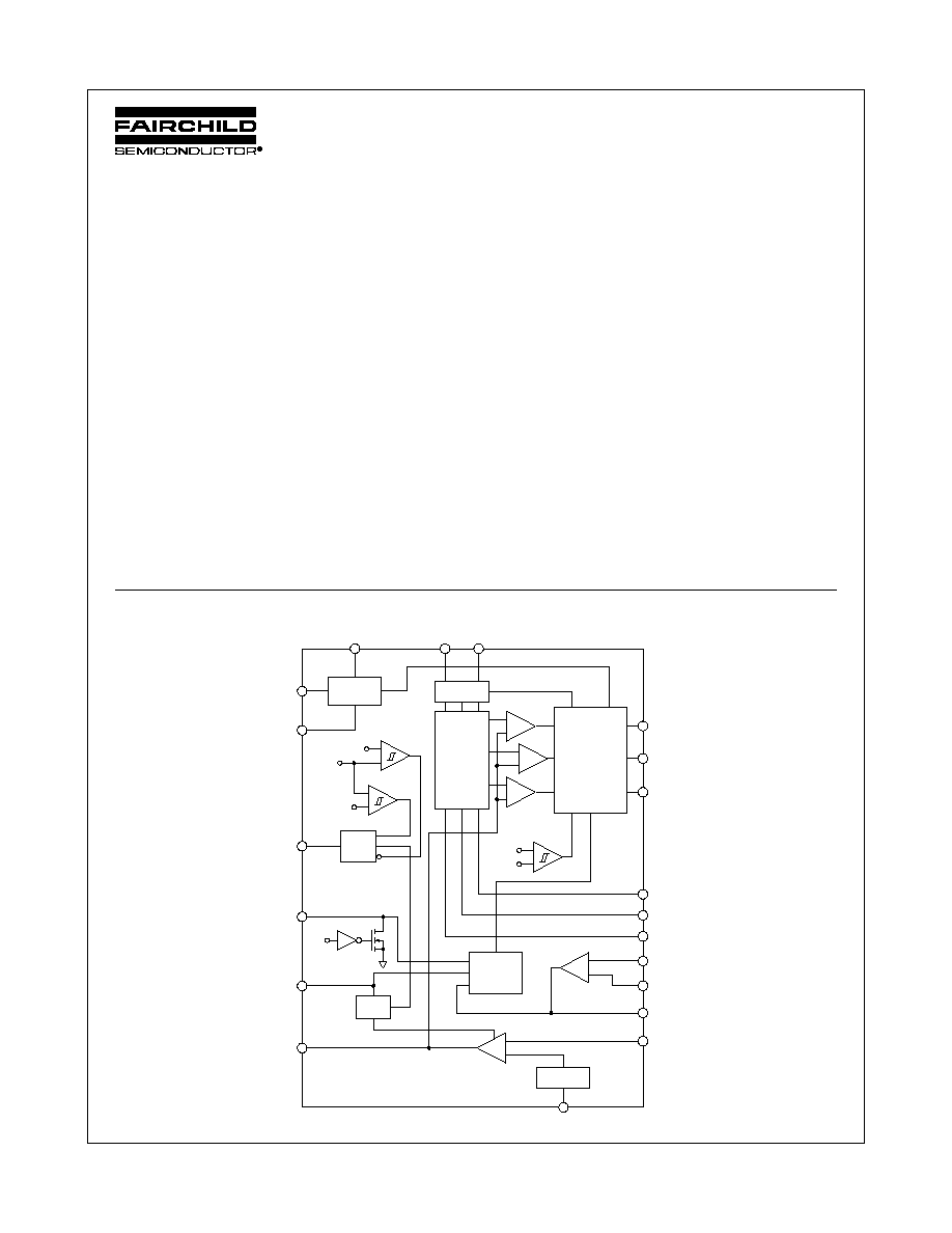
Block Diagram
VCC
800 mV
REFERENCE
SOFT
START
DELAY
UVLO
SHUTDOWN
& BIAS
OSCILLATOR
≠
+
GND
FAN5182
14
EN
6
DELAY
7
ILIMIT
10
PWRGD
5
1
RT
8
RAMPADJ
9
PWM2
19
3
FB
PWM3
18
SW1
17
CSSUM
12
CSCOMP
13
SW2
16
SW3
15
CSREF
11
PWM1
FBRTN
2
COMP
4
950mV
≠
+
1.05V
≠
+
650mV
+
≠
FB
FB
EN
CURRENT
LIMIT
CIRCUIT
CROWBAR
CURRENT
LIMIT
+
≠
CMP
+
≠
CMP
≠
+
+
≠
CMP
CURRENT
BALANCING
CIRCUIT
1/ 2 / 3-PHASE
DRIVER LOGIC
EN
SET
RESET
RESET
RESET
20

2
www.fairchildsemi.com
FAN5182 Rev. 1.0.1
F
AN5182 Adjustab
le Output 1,
2,
or 3-Phase Sync
hr
onous Buc
k Contr
oller
Pin Assignment
Pin Description
Pin #
Pin Name
Pin Description
1
VCC
Supply Voltage for the Device.
2
FBRTN
Feedback Return. Voltage error amplifier reference for remote sensing of the output voltage.
3
FB
Feedback Input. Error amplifier input for remote sensing of the output voltage. An external resistor
divider between the output and FBRTN connected to this pin sets the output voltage. This pin is also
the reference point for the power good and crowbar comparators.
4
COMP
Error Amplifier Output and Compensation Pin.
5
PWRGD
Power Good Output. Open-drain output that signals when the output voltage is outside the proper
operating range.
6
EN
Power Supply Enable Input. Pulling this pin to GND disables the PWM outputs and pulls the PWRGD
output low.
7
DELAY
Soft-Start Delay and Current Limit Latch-Off Delay Setting Input. An external resistor and capacitor
connected between this pin and GND set the soft-start ramp-up time and the overcurrent latch-off
delay time.
8
RT
Frequency Setting Resistor Input. An external resistor connected between this pin and GND sets the
oscillator frequency of the device.
9
RAMPADJ
PWM Ramp Current Input. An external resistor from the converter input voltage to this pin sets the
internal PWM ramp.
10
ILIMIT
Current Limit Setpoint/Enable Output. An external resistor connected from this pin to GND sets the
current limit threshold of the converter. This pin is actively pulled low when the FAN5182 EN input is
low, or when VCC is below its UVLO threshold, to signal to the driver IC that the driver high-side and
low-side outputs should go low.
11
CSREF
Current Sense Reference Voltage Input. The voltage on this pin is used as the reference for the cur-
rent sense amplifier. This pin should be connected to the common point of the output inductors.
12
CSSUM
Current Sense Summing Node. External resistors from each switch node to this pin sum the average
inductor currents together to measure the total output current.
13
CSCOMP
Current Sense Compensation Point. A resistor and a capacitor from this pin to CSSUM determine
the gain of the current sense amplifier.
14
GND
Ground. All internal biasing and the logic output signals of the device are referenced to this ground.
15≠17
SW3 To SW1
Current Balance Inputs. These are inputs for measuring the current level in each phase. The SW pins
of unused phases should be left open.
18≠20
PWM3 To PWM1
Logic-Level PWM Outputs. Each output is connected to the input of an external MOSFET driver such
as the FAN5009. Connecting the PWM3 output to GND causes that phase to turn off, allowing the
FAN5182 to operate as a 1- or 2-phase controller.
FAN5182
VCC
FBRTN
FB
COMP
PWRGD
EN
DELAY
RT
RAMPADJ
ILIMIT
PWM1
PWM2
PWM3
SW1
SW2
SW3
GND
CSCOMP
CSSUM
CSREF
1
2
3
20
19
18
4
8
10
5
6
7
13
16
15
14
9
11
12
17
QSOP-20L

3
www.fairchildsemi.com
FAN5182 Rev. 1.0.1
F
AN5182 Adjustab
le Output 1,
2,
or 3-Phase Sync
hr
onous Buc
k Contr
oller
Absolute Maximum Ratings (Note 1)
Recommended Operating Conditions
Notes:
1. Stresses above those listed under "Absolute Maximum Ratings" may cause permanent damage to the device. This is a stress rating
only and functional operation of the device at these or any other conditions above those indicated in the operational section of this
specification is not implied. Exposure to absolute maximum rating conditions for extended periods may affect device reliability.
Absolute maximum ratings apply individually only, not in combination. Unless otherwise specified all other voltages are referenced
to GND.
2. Junction to ambient thermal resistance,
JA
, is a strong function of PCB material, board thickness, thickness and number of copper
planes, number of via used, diameter of via used, available copper surface, and attached heat sink characteristics. Measured with
the device mounted on a board of FR-4 material, 0.063" thickness, no copper plane and zero airflow.
Parameter
Min.
Max.
Unit
VCC
-0.3
+15
V
FBRTN
-0.3
+0.3
V
EN, DELAY, ILIMIT, RT, PWM1-PWM3, COMP
-0.3
5.5
V
SW1-SW3
-5
+25
V
All Other Inputs and Outputs
-0.3
VCC + 0.3
V
Operating Junction Temperature, T
J
0
+125
∞C
Storage Temperature
-65
+150
∞C
Lead Soldering Temperature (10 seconds)
300
∞C
Lead Infrared Temperature (15 seconds)
260
∞C
Thermal Resistance Junction-to-Case, (
JC
)
38
∞C/W
Thermal Resistance Junction-to- Ambient, (
JA
) (Note 2)
90
∞C/W
Parameter
Min
Typ
Max
Unit
Supply Voltage Range
10.8
12
13.2
V
Operating Ambient Temperature
0
+85
∞C

4
www.fairchildsemi.com
FAN5182 Rev. 1.0.1
F
AN5182 Adjustab
le Output 1,
2,
or 3-Phase Sync
hr
onous Buc
k Contr
oller
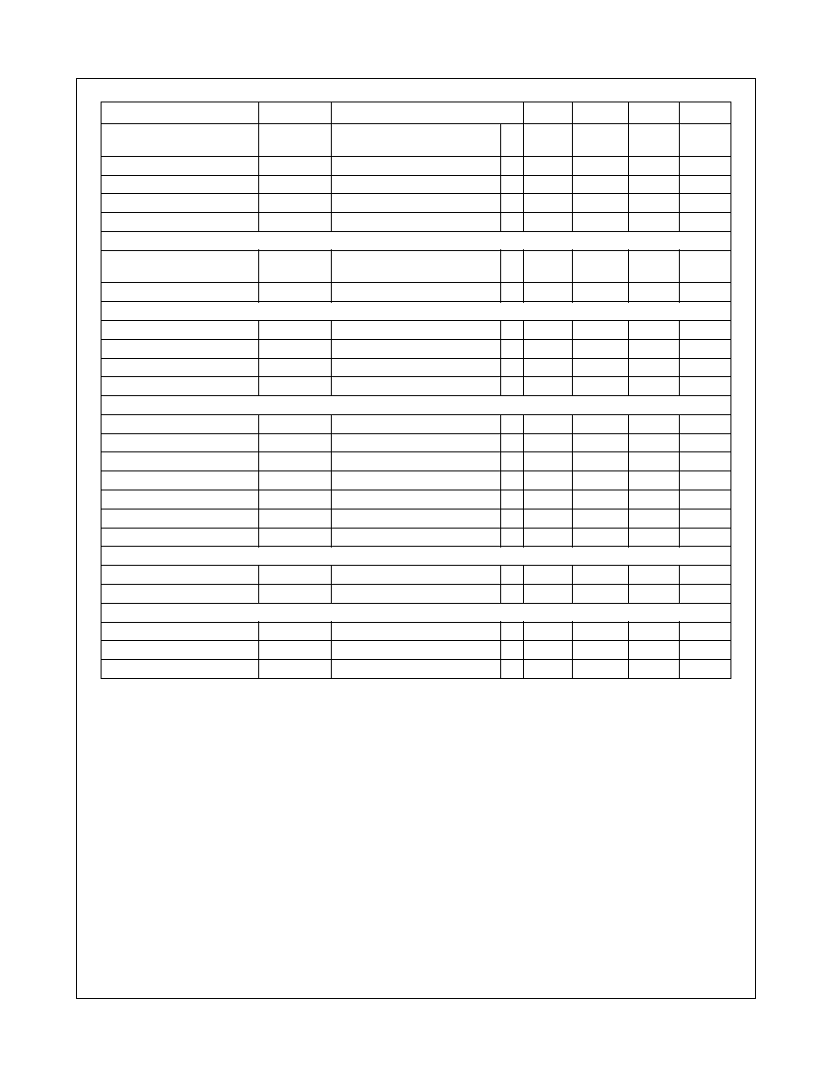
Electrical Characteristics
V
CC
= 12V, FBRTN = GND.
Indicates specifications over operating ambient temperature range. (Note 1)
Parameter
Symbol
Conditions
Min.
Typ.
Max.
Units
OSCILLATOR
Frequency Range
f
OSC
0.25
3
MHz
Frequency Variation
f
PHASE
R
T
= 332k
, 3-phase
T
A
= 25∞C, R
T
= 154k
, 3-phase
T
A
= 25∞C, R
T
= 100k
, 3-phase
155
200
400
600
245
kHz
Output Voltage
V
RT
R
T
= 100k
to GND
2.0
V
RAMPADJ Output Voltage
V
RAMPADJ
RAMPADJ - FB - 2K
x I
RAMPADJ
(with I
RAMPADJ
set to 20
µ
A)
-50
+50
mV
RAMPADJ Input Current
Range (Note 2)
I
RAMPADJ
0
100
µ
A
VOLTAGE ERROR AMPLIFIER
Output Voltage Low
0.3
V
Output Voltage High
3.1
V
Accuracy
V
FB
Referenced to FBRTN
784
800
816
mV
Input Bias Current
I
FB
FB = 800mV
-4
±1
+4
µ
A
Line Regulation
V
FB
V
CC
= 10V to 14V
0.05
%
FBRTN Current
I
FBRTN
100
140
µ
A
Output Current
I
O(ERR)
FB forced to V
OUT
- 3%
500
µ
A
DC Gain (Note 2)
87
dB
Gain Bandwidth Product
(Note 2)
G
BW(ERR)
COMP = FB
20
MHz
Slew Rate (Note 2)
C
COMP
= 10pF
10
V/
µ
s
CURRENT SENSE AMPLIFIER
Offset Voltage
V
OS(CSA)
CSSUM-CSREF ( See Figure 1.)
-5.5
+5.5
mV
Input Bias Current
I
BIAS(CSSUM)
-50
+50
nA
DC Gain (Note 2)
70
dB
Gain Bandwidth Product
(Note 2)
GBW
(CSA)
10
MHz
Slew Rate (Note 2)
C
CSCOMP
= 10pF
10
V/
µ
s
Input Common-Mode Range
CSSUM & CSREF
0
V
CC
-2.5
V
Output Voltage Low
0.1
V
Output Voltage High
V
CC
-2.5
V
Output Current
I
CSCOMP
500
µ
A
CURRENT BALANCE CIRCUIT
Common-Mode Range
(Note 2)
V
SW(X)CM
-600
+200
mV
Input Resistance
R
SW(X)
SW(X) = 0V
20
30
40
k
Input Current
I
SW(X)
SW(X) = 0V
4
7
10
µ
A
Input Current Matching
I
SW(X)
SW(X) = 0V
-7
+7
%
CURRENT LIMIT COMPARATOR
Output Voltage: Normal Mode
V
ILIMIT(NM)
EN > 2V, R
ILIMIT
= 250k
2.9
3
3.1
V
Output Voltage: Shutdown
Mode
V
ILIMIT(SD)
EN < 0.8V, I
ILIMIT
= -100
µ
A
400
mV
Output Current: Normal Mode
I
ILIMIT(NM
)
EN > 2V, R
ILIMIT
= 250k
12
µ
A
Maximum Output Current
60
µ
A
5
www.fairchildsemi.com
FAN5182 Rev. 1.0.1
F
AN5182 Adjustab
le Output 1,
2,
or 3-Phase Sync
hr
onous Buc
k Contr
oller
Notes:
1. All limits at operating temperature extremes are guaranteed by design, characterization and statistical quality control.
2. Guaranteed by design, not tested in production.
Current Limit Threshold
Voltage
V
CL
V
CSREF
- V
CSCOMP
, R
ILIMIT
=
250k
105
125
145
mV
Current Limit Setting Ratio
V
CL
/I
ILIMIT
10.4
mV/
µ
A
DELAY Normal Mode Voltage
V
DELAY(NM)
R
DELAY
= 250k
2.9
3
3.1
V
DELAY Overcurrent Threshold
V
DELAY(OC)
R
DELAY
= 250k
1.7
1.8
1.9
V
Latch-Off Delay Time (Note 2)
t
DELAY
R
DELAY
= 250k
,
C
DELAY
= 12nF
1.5
ms
SOFT-START
Output Current, Soft-Start
Mode
I
DELAY(SS)
During startup, DELAY < 2.4V
15
20
25
µ
A
Soft-Start Delay Time (Note 2)
t
DELAY(SS)
R
DELAY
= 250k
,
C
DELAY
= 12nF
500
µs
ENABLE INPUT
Input Low Voltage
V
IL(EN)
0.8
V
Input High Voltage
V
IH(EN)
2.0
V
Input Hysteresis Voltage
100
mV
Input Current
I
IN(EN)
-1
+1
µA
POWER GOOD COMPARATOR
Undervoltage Threshold
V
PWRGD(UV)
Relative to FBRTN
600
660
720
mV
Overvoltage Threshold
V
PWRGD(OV)
Relative to FBRTN
880
940
1000
mV
Ouput Low Voltage
V
OL(PWRGD)
I
PWRGD(SINK)
= 4mA
225
400
mV
Power Good Delay Time
200
ns
Crowbar Trip Point
V
CROWBAR
Relative to FBRTN
0.970
1.05
1.105
V
Crowbar Reset Point
Relative to FBRTN
550
650
750
mV
Crowbar Delay Point (Note 2)
t
CROWBAR
Overvoltage to PWM going low
400
ns
PWM OUTPUTS
Output Low Voltage
V
OL(PWM)
I
PWM(SINK)
= 400
µA
160
500
mV
Output High Voltage
V
OH(PWM)
I
PWM(SOURCE)
= -400
µA
4.0
5
V
SUPPLY
DC Supply Current
5
10
mA
UVLO THreshold Voltage
V
UVLO
V
CC
rising
6.5
6.9
7.3
V
UVLO Hysteresis
0.7
0.9
1.1
V
Parameter
Symbol
Conditions
Min.
Typ.
Max.
Units