 | –≠–ª–µ–∫—Ç—Ä–æ–Ω–Ω—ã–π –∫–æ–º–ø–æ–Ω–µ–Ω—Ç: FAN5231 | –°–∫–∞—á–∞—Ç—å:  PDF PDF  ZIP ZIP |

www.fairchildsemi.com
REV. 1.1.1 8/15/01
Features
∑ Provides 3 Regulated Voltages
≠ Microprocessor core (SpeedStepTM-enabled)
≠ Microprocessor I/O
≠ Microprocessor Clock Generator
∑ High Efficiency Over Wide Load Range
∑ Not Dissipative Current-Sense Scheme
≠ Uses MOSFET's R
DS(ON)
≠ Optional Current-Sense Resistor for Precision
Overcurrent
∑ Adaptive Dead Time Drivers for N-Channel MOSFETs
∑ Operates from +5V, +3.3V and Battery (5.6-24V) Inputs
∑ Precision Core Voltage Control:
≠ Remote "Kelvin" Sensing
≠ Summing Current-Mode Control
≠ On-Chip Mode-Compensated "Droop" for Optimum
Transient Response and Lower Processor Power
Dissipation
∑ TTL-Compatible 5-Bit Digital Output Voltage Selection
≠ Wide Range - 0.925VDC to 1.3VDC in 25mV Steps,
and from 1.3VDC to 2.0VDC in 50mV Steps
≠ Programmable "On-the-Fly" VID code change with
customer programmable slew rate and 100ms settling
time
∑ Power-Good Output Voltage Monitor
∑ No negative Core and I/O voltage on turn-off
∑ Over-Voltage, Under-Voltage and Over-Current Fault
Monitors
∑ 300kHz Fixed Switching Frequency
∑ Thermal Shut-Down
Applications
∑ Converters for Mobile Dual-Mode CPUs
∑ Web Tablets
∑ Internet Appliances
FAN5231
Precision Dual PWM Controller And Linear
Regulator for Notebook CPUs
Figure 1. Simplified Power System Diagram
+V
IN
V
OUT1
V
OUT2
V
OUT3
FAN5231
CORE
I/ O
PWM 2
LI NEAR
CONTROLLER
REGULATOR
PWM 1
CONTROLLER
CPU CLK
+V
IN
3.3V
VI D CODE

FAN5231
2
REV. 1.1.1 8/15/01
Description
The FAN5231 is a highly integrated power controller, which
provides a complete power management solution for mobile
CPUs. The IC integrates two PWM controllers and a linear
regulator as well as monitoring and protection circuitry into
a single 28-lead plastic SSOP package. The two PWM
controllers regulate the microprocessor core and I/O voltages
with synchronous-rectified buck converters, while the linear
regulator powers the CPU clock.
The FAN5231 includes 5-bit digital-to-analog converter
(DAC) that adjusts the core PWM output voltage from
0.925VDC to 2.0VDC and conforms to the Intel Mobile
VID specification. The DAC setting may be changed during
operation to accommodate Dual-Mode processors. Special
measures are taken to provide such a transition with con-
trolled rate in a specified 100 µs. A precision reference,
remote sensing, and a proprietary architecture with inte-
grated processor mode-compensated "droop" provide excel-
lent static and dynamic core voltage regulation. The second
PWM controller has a fixed 1.5V output voltage and powers
the I/O circuitry. Both PWM controllers have integrated
feedback-loop compensation that dramatically reduces the
number of external components. At nominal loads PWM
controllers operate at fixed frequency 300kHz. At light loads
when the filter inductor current becomes discontinuous,
controllers operate in a hysteretic mode. The out-of-phase
operation of two PWM controllers reduces input current
ripple in both modes of operation. The linear regulator uses
an internal pass device to provide 2.5V for the CPU clock
generator.
The FAN5231 monitors all the output voltages. A single
Power-Good signal is issued when soft start is completed
and all outputs are within ±10% of their respective set points.
A built-in over-voltage protection for the core and I/O out-
puts forces the lower MOSFETs on to prevent output volt-
ages from going above 115% of their settings. Under-voltage
protection latches the chip off when any of the three outputs
drops below 75% of the set value. The PWM controller's
overcurrent circuitry monitors the output current by sensing
the voltage drop across the lower MOSFETs. If precision
overcurrent protection is required, an external current-sense
resistor may be used.
Block Diagram
+
-
EA2
+
- 0.9V
VCC
BOOT1
VI D0
VI D1
VI D2
VI D3
DACO
UT
POWER-ON
RESET (POR)
TTL DAC
REFERENCE
SOFT START
VI D4 SOFT
VSEN1
UGATE1
PHASE1
LG ATE1
PGND1
VCC
LGDR1
HGDR1
GATE
CONTROL
VRET 1
+
-
+-
ISEN1
+-
LG ATE1
LG ATE1
+-
R1= 20k
+
-
OC LOGI C1
HI
LO
GATE L OGI C 1
OC COMP1
EA1
+
-
D
<
Q
Q
R
VCC
PWM ON
PWM /HYST
DEADT
RAMP 1
RAM P 2
CLK
VBATT
FL OGON
SHUTOFF
LG ATE2
+
+
-
CLAMP
OC L OGI C2
2.8V
+
-
D
<
Q
Q
R
VCC
BOOT2
UGATE2
PHASE2
LG ATE2
PGND2
VCC
LG DR2
HGDR2
GATE
CONTROL
HI
LO
GATE LOGI C 2
PWM ON
PWM /HYST
DEADT
FL OGON
SHUTOFF
+
-
LG ATE2
R1=20k
VSEN2
ISEN2
-
PWM
LATCH 1
FCCM
FCCM
PWM
LA TCH 2
OC COM P2
HYST ON
+
-
HY ST COM P1
HYST ON
DAC OUT
CL K 1
PRE AM P
+
-
HY ST COM P2
CLK2
CLK 2
CLK1
+
-
+
-
FFBK 1
DUTY CYCLE
GND
EN
PGOOD
OUTPUT
VOLTAGE
MO NIT OR
V3I N
VOUT3
+
+
-
0.9V
-
L I NEAR REGULA TOR
OVP1
OVP2
OVP1
OVP2
DYNA MI C
CLAMP
DUTY CYCLE
DYNAM I C
LO GI C 1
MO DE
CONTROL
PHASE1
FFBK 1
LO GI C 1
MO DE
CONTROL
FAST FEEDBACK COMP 1
COMP 2
MO DE
CONTROL
PHASE1
FAN5231
REV. 1.1.1 8/15/01
3
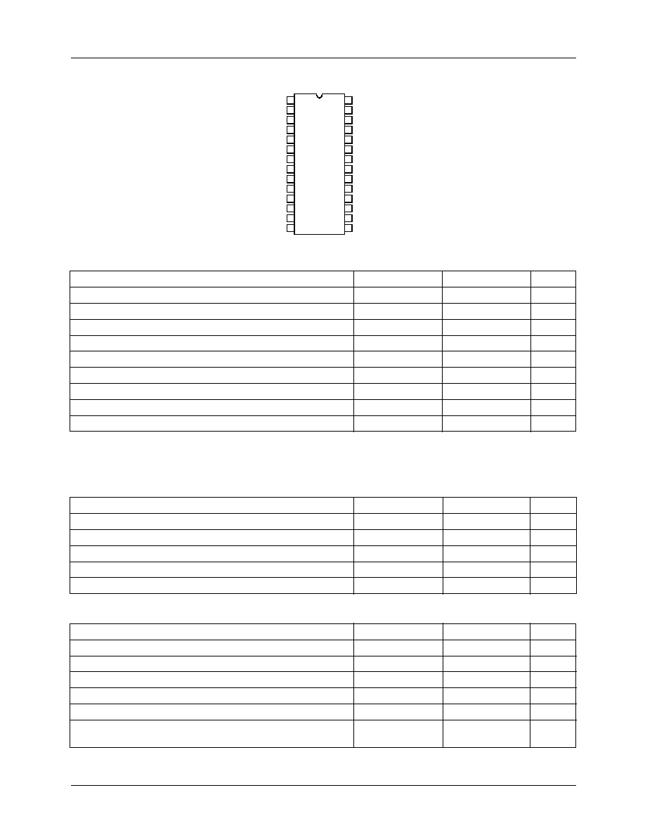
Pinout
Absolute Maximum Ratings
CAUTION:
Stresses above those listed in "Absolute Maximum Ratings" may cause permanent damage to the device. This is a
stress only rating and operation of the device at these or any other conditions above those indicated in the operational sections
of this specification is not implied.
Recommended Operating Conditions
Thermal Information
Note
1.
JA
is measured with the component mounted on an evaluation PC board in free air.
Parameter
Min.
Max.
Units
Supply Voltage, V
CC
+ 6.5
V
Input Voltage, Vin
+ 29.0
V
V3in
+ 6.5
V
PHASE1,2
+ 29.0
V
BOOT1,2
+ 29.0
V
BOOT1,2 with respect to PHASE1,2
+ 6.5
V
PGOOD, RT/FAULT, and GATE Voltage
GND - 0.3
V
CC
+ 0.3
V
Core Output or I/O Voltage
GND - 0.3
+ 6.5
V
ESD Classification
Class 2
Parameter
Min.
Max.
Units
Supply Voltage, V
CC
+5.0 ±5%
V
Input Voltage, Vin
+7.5
22.0
V
V3in
+3.3 ±10%
V
Ambient Temperature Range
-20
85
∞C
Junction Temperature Range
-20
125
∞C
Parameter
Min.
Max.
Units
Thermal Resistance (Typical, Note 1)
JA
(∞C/W)
QSOP Package
55
QSOP Package (with 3 in
2
of copper)
TBD
Maximum Junction Temperature (Plastic Package)
150
∞C
Maximum Storage Temperature Range
-65
150
∞C
Maximum Lead Temperature (Soldering 10s)
(QSOP - Lead Tips Only)
300
∞C
LG ATE2
PGND2
BOOT2
UGATE2
VI D1
VI D0
VSEN2
V3I N
VOUT3
VCC
UGATE1
BOOT1
PGND1
SOFT
EN
VSEN1
VRET 1
GND
L GATE1
28
27
26
25
24
23
22
21
20
19
18
17
16
15
1
2
3
4
5
6
7
8
9
10
11
12
13
14
VI D3
PHASE2
VI D2
ISEN1
VI N
ISEN2
VI D4
PHASE1
PGOOD

FAN5231
4
REV. 1.1.1 8/15/01
Electrical Specifications
(Recommended Operating Conditions, Unless Otherwise Noted. Refer to Figures 1, 2 and 3)
Parameter
Symbol
Test Condition
Min.
Typ. Max Units
VCC Supply
Nominal Supply Current
I
CC
GATE1, GATE2 Open
≠
2
2.5
mA
Shut-down Supply Current
I
CCS
≠
30
50
µA
Battery Pin Supply Current
I
VIN
≠
≠
100
µA
Battery Pin Leakage Current at
Shut-Down
I
VINSD
≠
≠
5
µA
Power-On Reset
Rising VCC Threshold
4.3
4.5
4.6
V
Falling VCC Threshold
3.9
4.1
4.3
V
Oscillator
Free Running Frequency
255
300
345
kHz
Ramp Amplitude, pk-pk
Vbat = 16V
≠
2
≠
V
Ramp Offset
≠
0.5
≠
V
Reference, DAC and Soft Start
VID0-VID4 Input Low Voltage
≠
≠
0.8
V
VID0-VID4 Input High Voltage
2.0
≠
≠
V
VID0-VID4 Pull-up Current to VCC
≠
1
≠
µA
DAC Voltage Accuracy
Measured at pin 18
-1.0
≠
+1.0
%
Soft-Start Current During Start-Up
I
SS
VSS = 0V...0.9V
18
27
36
µA
Soft-Start Current During Mode
Change
I
SSM
VSS = 0.925V...2.0V
350
500
650
µA
Enable
Enable Voltage Low
V
ENLOW
IC Inhibited
≠
≠
0.8
V
Enable Voltage High
V
ENHIGH
IC
Enabled
Input has internal pull-up current
source 2µA typ
2.0
≠
≠
V
PWM 1 Converter
Output Voltage
VOUT1
Defined by the current VID code
(Table 1)
0.925
≠
2.0
V
Static Load Regulation
100mA < I
VOUT1
< 15.0A
-2.0
≠
+2.0
%
Under-Voltage Shut-Down Level
V
UV1
Percent of the voltage set by VID
code. Disabled during dynamic VID
code change.
70
75
80
%
Under-Voltage Shut Down Delay
T
DOC1
≠
1.4
≠
µs
Over-Voltage
V
OVP1
Percent of the voltage set by VID
code.
110
115
120
%
Over-Voltage Shut Down Delay
T
DOV1
≠
2.4
≠
µs
Over-Current Comparator
Threshold
I
OC1
100
135
170
µA
PWM 2 Converter
Output Voltage
VOUT2
1.5
V
Load Regulation
100mA < I
VOUT3
< 2.1A
-2.0
≠
+2.0
%
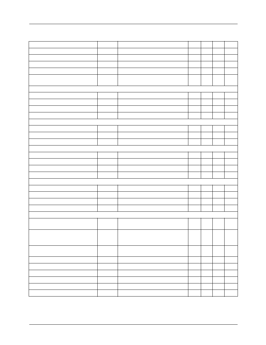
FAN5231
REV. 1.1.1 8/15/01
5
Under-Voltage Shut-Down Level
V
UV2
1.05
≠
1.20
V
Under-Voltage Shut Down Delay
T
DOC2
≠
1.4
≠
µs
Over-Voltage Shut-Down
V
OVP2
1.65
≠
1.80
V
Over-Voltage Shut Down Delay
T
DOV2
≠
2.4
≠
µs
Over-Current Comparator
Threshold
I
OC2
100
135
170
µA
Linear Regulator
Output Voltage
VOUT3
2.5
V
Load Regulation
10mA < I
VOUT3
< 150mA
-2.0
≠
2.0
%
Under-Voltage Shut-Down Level
V
UV3
1.8
≠
2.0
%
Current Limit
I
OC3
190 250
340
mA
PWM Controller Error Amplifiers
DC Gain
By design
≠
86
≠
dB
Gain-Bandwidth Product
GBWP
By design
≠
2.7
≠
MHz
Slew Rate
SR
By design
≠
1
≠
V/µs
PWM 1 Controller Gate Drivers
Upper Drive Pull-Up Resistance
R
1UGPUP
≠
6
8
Upper Drive Pull-Down Resistance R
1UGPDN
≠
3
5
Lower Drive Pull-Up Resistance
R
1LGPUP
≠
6
8
Lower Drive Pull-Down Resistance R
1LGPDN
≠
0.8
1.5
PWM 2 Controller Gate Drivers
Upper Drive Pull-Up Resistance
R
2UGPUP
≠
12
20
Upper Drive Pull-Down Resistance
R
2UGPDN
≠
6
10
Lower Drive Pull-Up Resistance
R
2LGPUP
≠
10
20
Lower Drive Pull-Down Resistance R
2LGPDN
≠
6
10
Power Good
V
OUT1
Upper Threshold
Percent of the voltage defined by the
VID code
108
≠
114
%
V
OUT1
Lower Threshold, Falling
Edge
Percent of the voltage defined by the
VID code
85
≠
92
%
V
OUT1
Lower Threshold, Risisng
Edge
Percent of the voltage defined by the
VID code
87
≠
94
%
V
OUT2
Upper Threshold
1.60
≠
1.75
V
V
OUT2
Lower Threshold
1.30
≠
1.45
V
V
OUT3
Upper Threshold
2.65
≠
2.85
V
V
OUT3
Lower Threshold
2.15
≠
2.35
V
PGOOD Voltage Low
V
PGOOD
I
PGOOD
= -1.6mA
≠
≠
0.4
V
PGOOD Leakage Current
I
PGlLKG
V
PULLUP
= 5.0V
≠
≠
1.0
µA
Electrical Specifications
(Continued)
(Recommended Operating Conditions, Unless Otherwise Noted. Refer to Figures 1, 2 and 3)
Parameter
Symbol
Test Condition
Min.
Typ. Max Units