 | –≠–ª–µ–∫—Ç—Ä–æ–Ω–Ω—ã–π –∫–æ–º–ø–æ–Ω–µ–Ω—Ç: FAN5232 | –°–∫–∞—á–∞—Ç—å:  PDF PDF  ZIP ZIP |

www.fairchildsemi.com
REV. 1.1.1 10/7/02
Features
∑ Three outputs: Adjustable Buck, 3.3V-Always,
5V-Always
∑ Adjustable synchronous switcher, 5V ≠ 80% Vin
∑ 1% internal reference precision
∑ Current mode with voltage feed-forward
∑ Precision current limit option
∑ Charge pump works at all loads
∑ No shoot-through current
∑ Independent shutdown pins for ACPI
∑ Power Good, input UVLO, output OV
∑ 5.6V to 24V input voltage range
Applications
∑ LCD PCs
∑ Notebook PCs and PDAs
∑ Hand-held portable instruments
Description
The FAN5232 is a high efficiency and high precision DC/DC
controller for PCs. It has a synchronous switcher whose
output can be adjusted from 5V up to 80% of Vin. It also has
two linear regulators for standby, 3.3V and 5V. The PWM
utilizes both input and output voltage feedback in a
current-mode control, allowing for fast and stable loop
response over a wide range of input and output variations.
Synchronous switching provides best efficiency over a wide
range of loads. Current sense based on MOSFET R
DS,on
gives maximum efficiency, while also permitting use of an
optional sense resistor for high precision.
The FAN5232 is available in a 14 pin TSSOP package.
Block Diagram
1
2
3
4
5
6
7
14
13
12
11
10
9
8
FAN5232
Vin = 16≠22V
SDNADJ
3.3V-Always
5V-Always
SDWN
PWRGD
12V @ 8A
+
FAN5232
Adjustable PWM Buck Controller for LCD PCs

FAN5232
PRODUCT SPECIFICATION
2
REV. 1.1.1 10/7/02
Pin Assignments
Pin Description
Absolute Maximum Ratings
1
Note:
1. Functional operation under any of these conditions is NOT implied. Performance and reliability are guaranteed only if
Operating Conditions are not exceeded.
Pin Number
Pin Name
Pin Function Description
1
VBATT
Battery Voltage.
Battery voltage sensor.
2
3V_ALWAYS
3.3V-ALWAYS Linear Regulator.
Total load current on pins 2 and 3 together
must not exceed 50mA.
3
5V_ALWAYS
5V-ALWAYS Linear Regulator.
Total load current on pins 2 and 3 together
must not exceed 50mA.
4
AGND
Analog Ground.
5
SDWN
IC Shutdown.
Puts entire chip into shutdown. OFF=0. ON=1.
6
SDNADJ
Shutdown and Softstart for the Switcher.
OFF=0. ON=1.
7
PWRGD
Switcher Output OK.
An open collector output that will be low if the switcher
output is out of spec.
8
VFBSW
Voltage Feedback for the Switcher.
9
PGND
Ground for the Switcher.
Connect by the shortest possible path to the source
of the low side MOSFET.
10
LSD
Low Side FET Driver for the Switcher.
Connect this pin through a resistor to
the gate of an N-channel MOSFET.
11
SW
High Side FET Source and Low Side FET Drain Switching Node.
12
ISNS
Current Feedback for the Switcher.
Connect by the shortest possible path to
a resistor connected to the drain of the low side MOSFET.
13
HSD
High Side FET Driver for the Switcher.
Connect this pin through a resistor to
the gate of an N-channel MOSFET.
14
CPUMP
Charge Pump for the Switcher.
Generates gate drive voltage for the high-side
MOSFET.
Parameter
Conditions
Min.
Typ.
Max.
Units
VBATT Pin
-0.3
29
V
PHASE, IFB, SDWN Pins
-5
29
V
CPUMP, HSD Pins
-0.3
34
V
All Other Pins
-0.3
6.5
V
Thermal Resistance,
J-A
J-C
100
32
∞C/W
∞C/W
Junction Temperature
150
∞C
Storage Temperature
-65
150
∞C
Lead Temperature, Soldering 10 sec.
300
∞C
1
2
3
4
5
6
7
14
13
12
11
10
9
8
VBATT
3V_ALWAYS
5V_ALWAYS
AGND
PWRGD
CPUMP
HSD
ISNS
SW
LSD
PGND
VFB
SDWN
SDNADJ

PRODUCT SPECIFICATION
FAN5232
REV. 1.1.1 10/7/02
3
Recommended Operating Conditions
Parameter
Conditions
Min.
Typ.
Max.
Units
VBATT Voltage
5.6
24
V
Ambient Temperature
-20
85
∞C
Electrical Specifications
(V
BATT
= 16V, T
A
= -20 to 85∞C, circuit of Figure 1, unless otherwise specified.)
Parameter
Conditions
Min.
Typ.
Max.
Units
Supply
V
CC
Input Quiescent Current
H/LSD
Open
1.4
mA
Stand-by
60
µA
Shut-down
10
µA
V
CC
Input UVLO Threshold
Rising
4.3
4.5
5.1
V
Falling
4.0
4.3
4.7
Switcher
Output Voltage Precision, VFB
0.1
I
5.5A, 7.2
VBATT
24V
4.900
5
5.100
V
I
100mA, 5.6
VBATT
24V
4.900
5
5.100
Oscillator Frequency, f
OSC
255
300
345
KHz
Gate Drive On-Resistance for
all Sources and HSD Sinks
6
12
Gate Drive On Resistance for
LSD Sink
1.5
8
HSD On Output, V
CPUMP
-V
GS
I = 10µA
100
mV
HSD Off Output, V
GS
I = -10µA
100
mV
LSD On Output, V
5V-Always
-V
GS
I = 10µA
100
mV
LSD Off Output, V
GS
I = -10µA
100
mV
Ramp Amplitude, pk-pk
2
V
Ramp Offset
0.5
V
Ramp Gain from VBATT
125
mV/V
Error Amplifier GBW
3
MHz
Current Limit Threshold
R3 = 1K
135
150
165
mV
Over Voltage Threshold
2µs delay
110
115
120
%V
O
Under Voltage Threshold
2µs delay
70
75
80
%V
O
Max Duty Cycle
80
%
Min HSD On-time
200
nsec
VFBSW, ISNS Input Leakage
Current
100
200
nA
SDN/SS Full On Voltage Min.
4.2
V
SDN/SS Full Off Voltage Max.
800
mV
5V and 3.3V Always
Linear Regulator Accuracy
5.6V
VBATT
22V,
0
ILOAD
50mA
-3.3
2
%
Rated Output Current
I
3.3
+ I
5
50
mA
Overcurrent Limit
2µs delay
100
180
mA
Undervoltage Threshold
2µs delay
70
75
80
%
FAN5232
PRODUCT SPECIFICATION
4
REV. 1.1.1 10/7/02
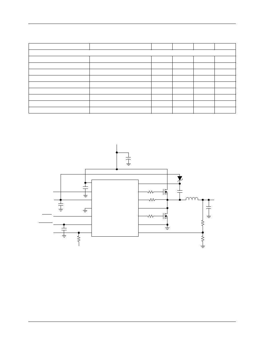
Application Circuit
Figure 1. Application Circuit for LCD PC Main Power
Control and Signal Functions
Control Logic Low
600
mV
Control Logic High
2
V
Softstart Current
3
5
7
µA
Over-temperature Shutdown
150
∞C
Over-temperature Hysteresis
25
∞C
PWRGD Threshold
-14
-12
-9
%V
O
PWRGD Saturation Voltage
I
sink
= 4mA
400
mV
PWRGD Leakage Current
V
CC
= 5.5V
1
µA
PWRGD Pulse Width for Trip
Low
High, High
Low
5
10
µsec
Electrical Specifications
(Continued)
(V
BATT
= 16V, T
A
= -20 to 85∞C, circuit of Figure 1, unless otherwise specified.)
Parameter
Conditions
Min.
Typ.
Max.
Units
1
2
3
4
5
6
7
14
13
12
11
10
9
8
U1
FAN5232
Vin = 16≠22V
SDNADJ
3.3V-Always
C2
C3
Q1
Q2
R3
R2
R4
R5
R6
C6
L1
C5
D1
5V-Always
SDWN
PWRGD
12V @ 8A
C4
R1
5V
+
C1
+

PRODUCT SPECIFICATION
FAN5232
REV. 1.1.1 10/7/02
5
Table 1. RC5232 Application Bill of Materials
Reference
Manufacturer, Part #
Quantity Description
Comments
C1
SANYO
25SV47M
1
47µF, 25V
OSCON, I
rms
= 3.5A
C2-5
Any
4
100nF, 50V
Ceramic
C6
AVX
TPSE227M016#0100
1
220µF, 16V
Tantalum, ESR=100m
R1
Any
1
10K
, 1%
R2, R4
Any
2
4.7
, 1%
R3, R5
Any
2
1K
, 1%
R6
Any
1
715
, 1%
D1
Fairchild
MBR0540L
1
500mA, 40V Schottky
L1
Coiltronics
UP2B-1R5
1
1.5µH, 8.3A
R < 8m
Q1
Fairchild
FDS6690A
1
30V N-channel MOSFET
R = 20m
@ V
GS
= 4.5V
Q2
Fairchild
FDS6680S
1
30V N-channel MOSFET
with Integrated Schottky
R = 17m
@ V
GS
= 4.5V
U1
Fairchild FAN5232
1
Controller
Application Information
Overview
The FAN5232 is a high efficiency and high precision DC/DC
controller for LCD PCs and portable applications. It provides
a switcher controller capable of generating a voltage between
5V to 80% of Vin, and a 5V and a 3.3V linear regulator for
standby applications. The controller has a power good output
and an enable/soft start to permit proper system sequencing.
Initialization
The FAN5232 automatically initializes upon receipt of input
power. The Power-on Reset (POR) function continually
monitors the input supply voltage on the V
CC
pin and
initiates soft start operation after the input supply voltage
exceeds 4.5V. Should this voltage drop below 4.0V, POR
disables the chip.
Soft Start
When soft start is initiated by POR, and if the SDWN pin is
not held low, the voltage on the SDNADJ pin begins ramping
up, with the rate of rise set by the external capacitor on the
pin. Below 700mV, the output is off. Between 700mV and
1.6V, the output is allowed to linearly ramp up. Above 1.6V,
the output is fully enabled, and regulates.
Shutdown
There are two separate shutdown pins to provide output
power control ≠ SDWN, and SDNADJ. Taking the SDNADJ
pin low will disable the switcher output and reset the output's
internal latches for short circuit, under-voltage and over-volt-
age. Taking the SDWN pin low puts the entire chip in shut-
down. Each of the SDN pins has an internal
pull-up.
Switcher Architecture
Overview
The switcher output of the FAN5232 is generated from the
unregulated input (battery) voltage using a synchronous buck
converter. Both high-side and low-side MOSFETs are
N-channel.
The converter has pins for current sensing using the low-side
MOSFET R
DS,on
; a pin for voltage-sense feedback; a pin
that enables the converter and permits soft-start; a power
good pin; and a pin for generating the boost voltage to drive
the high-side MOSFET.