 | –≠–ª–µ–∫—Ç—Ä–æ–Ω–Ω—ã–π –∫–æ–º–ø–æ–Ω–µ–Ω—Ç: FAN5236 | –°–∫–∞—á–∞—Ç—å:  PDF PDF  ZIP ZIP |
Application Bulletin AB-28
Power Conversion for the Data
Communications Market
www.fairchildsemi.com
REV. 1.0.0
1
Abstract
This application bulletin discusses the transition from tradi-
tional telephony to converged voice and data over Internet
Protocol (IP) and its implications for the power conversion
of such systems. A few power conversion examples are pro-
vided complete of applications schematics.
Introduction
The arm wrestling between voice and data has concluded in
favor of the latter with all the major players now posturing
for leadership of the migration from traditional voice to
Internet Protocol (IP) telephony. On the short term the huge
investments in both traditional telephony infrastructure and
data over IP warrants that over the next few years we will
have to provide power conversion for both types of systems
as well as for the converged systems to come.
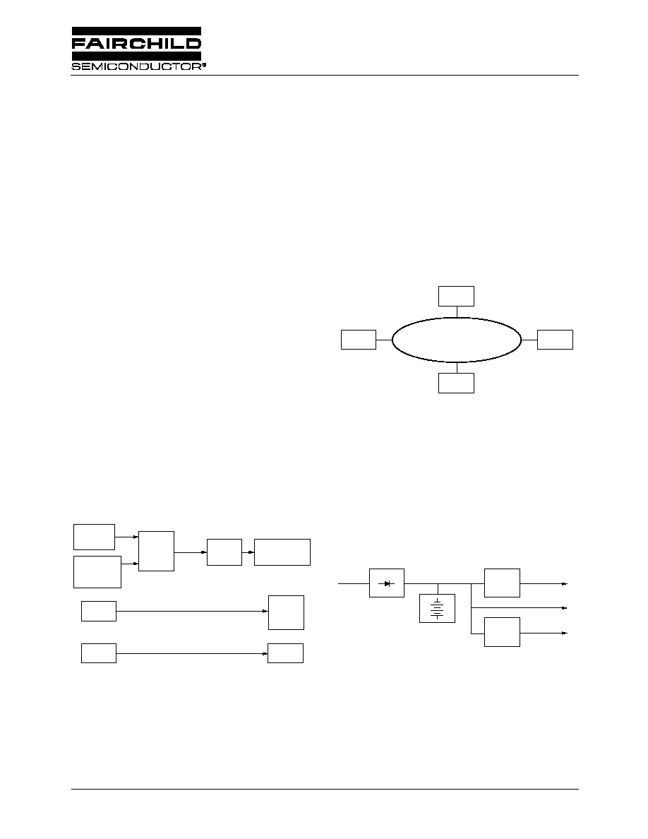
Current Environment with Separate
Networks
Fig. 1 shows the current situation with voice going through
traditional PBX (Private Branch Office), Central Office, and
Switch to the Public Switch Telephone Network (PSTN). On
independent paths the data travels from Routers to wide Area
Networks (WAN) and the video goes trough a third indepen-
dent path.
Fig.1. Separate Networks for Voice, Data and Video
Migration to Converged Voice/
Data IP
Fig. 2 shows the envisioned converged Voice/Data/Video
system over IP. At the center of this new universe is the
Internet Protocol Wide Area Network, with all the services,
including voice, data, video and wireless communications
gravitating around it.
Fig. 2. Voice/Data/video Over IP
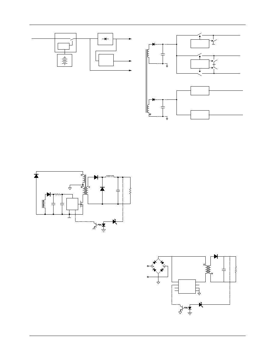
Telecom ≠48V DC Power Distribution
Traditionally telecom systems have been distributing a DC
power (-48V typically) obtained from a battery back up
being continually charged by a Rectifier/Charger from the
AC line. Subsequently the ≠48V is converted into various
low positive DC voltages (Fig. 3 shows 12V only for
simplicity) as well as back to AC voltages as necessary.
Fig. 3. Telecom ≠48V DC power distribution
Datacom AC Power Distribution
Data centric systems tend to rely on an Uninterruptible
Power Supply (AC UPS) front-end for distributing AC
power, which subsequently is converted into the basic
constituents, -48V, AC power and low voltage DC (again,
for simplicity we are only showing a 12V DC in Fig. 4).
Home
Phone/Fax
Wide Area
Network
(WAN)
Router
Video
Video
Video
Voice
Switch
Central
Office
Data
Office PBX
(Private Branch
Exchange)
Public Switch
Telephone
Network (PSTN)
Video
Router
WLAN
IPWAN = Internet Protocol Wide Area Network
WLAN = Wireless Local Area Network
PSTN = Public Switched Telephone Network
IP WAN
PSTN
DC/AC
DC/DC
Battery
Backup
Rectifier
/Charger
-48V
AC LINE
12V DC
-48V
120/208V AC
AB-28
APPLICATION BULLETIN
2
7/18/02
Fig.4. Datacom AC Power Distribution
With the advent of the converged systems, these separate
approaches to power distribution will converge into new
architectures but the bottom line is that at the board or back-
plane level the usual voltages will need to be delivered,
namely 12V and 5V, as well as 0.9V, 1.8V, 2.5V, 3.3V with
more to come.
The delivery of such low voltages starting from DC or AC
power will be the focus of this document from here on.
DC-DC conversion
Fig. 5 shows the ≠48V to +Vout (+5, +12V etc.) with a
forward converter architecture based on the ML4823 high
frequency PWM controller:
Fig. 5. ≠48V to +Vout Conversion
Fig.6 shows the DC-DC conversion from 12V and 5V down
to a slew of typical low voltages required by modern
electronic loads.
Fig. 6. DC-DC Conversion Diagram
The conversion down to heavy loads is done with
synchronous rectification switching regulators of single or
multiphase interleaved type, while for lighter loads
linear regulators can be utilized.
AC-DC conversion
Fig. 7 shows the conversion of AC power directly down to
one of the DC voltages listed earlier, all low enough to be
safely distributed on the motherboard. The AC line is
rectified first by means of a full bridge diode rectifier that
converts the alternate AC voltage into a continuous but still
poorly regulated intermediate voltage. Next this voltage is
converted down to a low voltage usable by the electronics on
the motherboard by means of a "fly-back" converter
(KA5x03xx family) with minimum number of external
components. This conversion requires electrical isolation
between the high input and the low output voltages: this is
accomplished via the utilization of a transformer (T) in the
forward conversion path and an opto-coupler in the feedback
path.
Fig .7. AC/DC Conversion Diagram
DC/DC
AC LINE
AC UPS
AC
DC/AC
Rectifier
Battery
Backup
12V DC
-48V
120/208V AC
UF4005
Lreset
Rload
MBR
3060PT
MBR3060PT
Lbias
C1
C2
C3
+Vout
L
D1
D2
D3
T
ML4823
H11A817A
RC431A
Rlim
-48V
-48V
2
FAN5092
TSSOP28
FAN5236 Dual
S024/28
LDO RC1587
LDO RC1585
D1
12V
5V
C1
C1
T1
N:1
Vout1: 1-5V, 30A
Vout2: 2.5V, 6A
Vout3: 1.8V, 6A
Vout4: 3.3V, 3A
Vout5: 1.5V, 5A
Rload
C2
Vout
1N5822
Vstart
FB
GND
GND
Drain
Vcc
GND
GND
AC Line
+
≠
T
H11A817A
RC431A
KA5H0365
MB6S
APPLICATION BULLETIN
AB-28
REV. 1.0.0
3
An integrated version of the opto-coupler (H11A817A) and
secondary voltage reference (RC431A) is also available
(FOD2712).
In the following sections we dive into some details of the
conversion from 12V and 5V down to final electronic load
voltage.
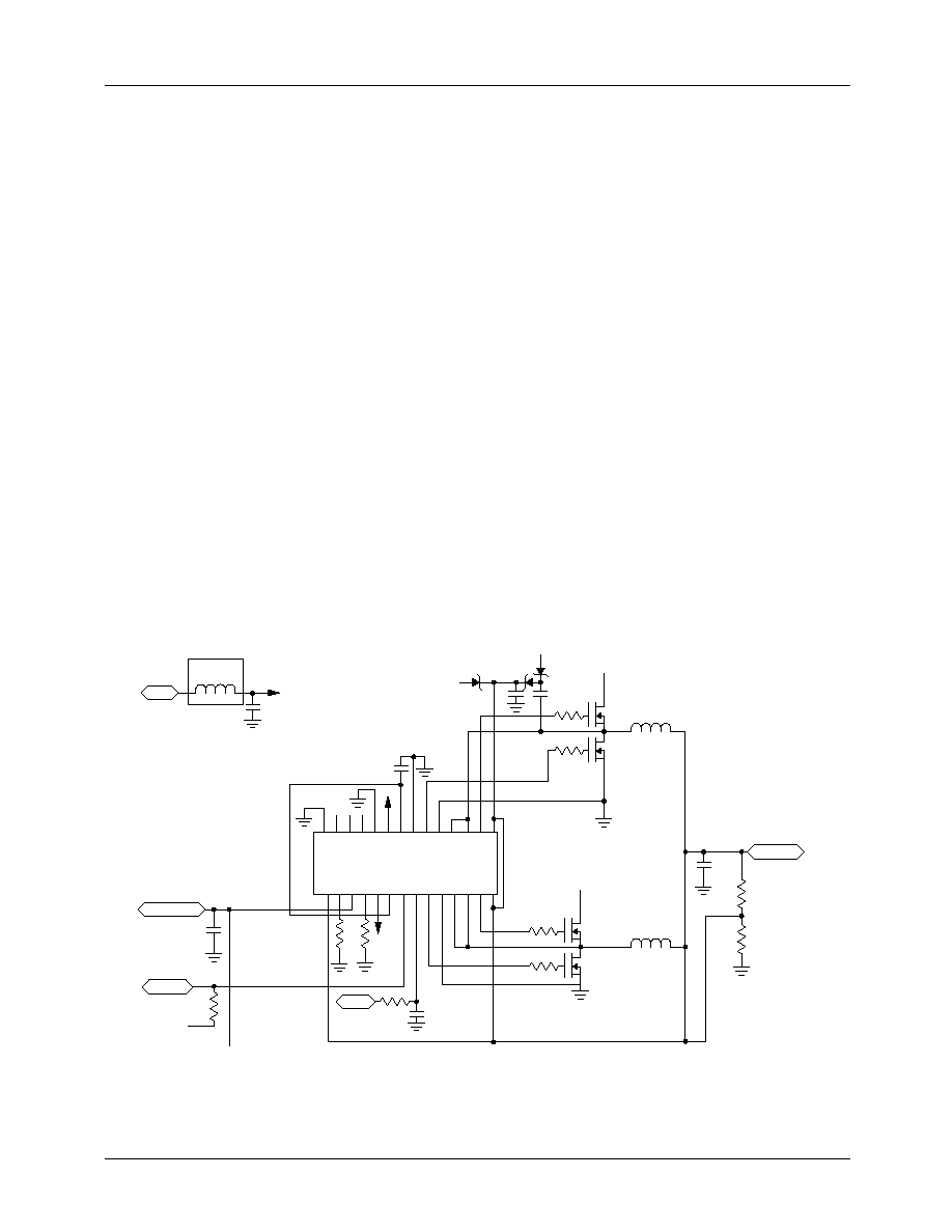
FAN5092 Two-Phase Interleaved
Buck Converter
The FAN5092 step-down (buck) converter is ideal for data
communications applications. This IC is a two-phase inter-
leaved buck converter switching up to 1MHz per phase. The
application diagram illustrates conversion from 12Vdown to
3.3V in a 12V-only input voltage source environment. The
chip integrates the controller and the drivers on a single die.
The high frequency of operation is enabled by:
∑ The monolithic approach of integrating controller and
drivers on board
∑ A fast proprietary "leading edge valley control"
architecture with 100ns of response time
∑ The strongest drivers in the industry at 1
of source and
sink impedance for both high and low side driver of each
phase
Such combination of features, together with loss-less current
sensing via R
DSON
sense, allows for a very efficient delivery
of power with very small passive components leading to new
record levels of power density.
The application diagram of the IC is shown in Fig 8 for a
3.3V, 30A load. Optimum companions of the FAN5092 are
the Fairchild discrete DMOS FDB6035AL for high side pass
transistors Q1,2 and FDB6676S for low side synchronous
rectification transistors Q2,4.
Two FAN5092 can be paralleled by means of doubling the
above application and connecting together two pins (pin 26
and pin 15). This will allow handling of loads up to 120A.
Fig. 8. FAN5092 Application Circuit
+12V
+12V
+12V
+12V
+12V
+12V
3.3V
30A
R16
R17
ENABLE/SS
PWRGD
+12V
D1
D2
C2
C1
C3
R1
R4
R2
R7
R8
R3
A
1 2
3
4 5 6 7 8 9 10 11 12 13 14
28 27 26 25 24 23 22 21 20 19 18 17 16 15
+5V
D3
C5
R5
Q1
Q3
Q4
L2
L3
X
C
OUT
C
IN
L1 (Optional)
U1
FAN5092
Q2
D3=8.2V
R6
C4
AB-28
APPLICATION BULLETIN
4
7/18/02
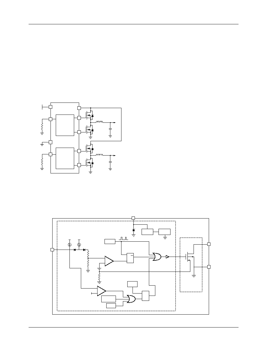
FAN5236 Dual Synchronous Buck
Converter
The FAN5236 PWM controller (Fig. 9) provides high
efficiency and regulation for two output voltages adjustable
in the range from 0.9V to 5.5V. Synchronous rectification
and hysteretic operation at light loads contribute to a high
efficiency over a wide range of loads. The hysteretic mode
of operation can be disabled separately on each PWM
converter if PWM mode is desired for all load levels. Again
high efficiency is obtained by using MOSFET's RDSON for
current sensing. Out-of-phase operation with 180-degree
phase shift reduces input current ripple.
Fig. 9. FAN5236 Block Diagram
RC1585/7 Linear Regulators
In some cases if the input to output voltage difference is sen-
sibly less than the output voltage it make sense to use linear
regulators. In Fig.6 Fairchild's RC1587, 3A and RC1585, 5A
linear regulators are showcased.
KA5H0365 Offline Converter
The high level of simplicity of the AC/DC converter in Fig. 6
is possible thanks the multi-chip approach to integration of
the this controller family (Fig. 10). The TO220 package
houses two dies, a controller die and a high voltage MOS-
FET die on board. Here again power hungry discrete current
sense resistors are avoided, in this case by means of a ratioed
sense-fet technique on board of the discrete element.
For more details and a complete bill of materials please refer
to the FAN5092, FAN5236, RC1585, RC1587 and FOD2712
data sheets available on the Fairchild web site.
For KA5H0365 please refer to the data sheet as well as to
FPS Application Notes for SMPS design available on the
Fairchild web site.
Conclusion
The merging of data, voice and video blurs the line between
computing and communications. The smart loads of either
application draw from the same advanced, high-density sub-
micron low voltage CMOS technologies and require similar
solutions for distributed power conversion. Fairchild exper-
tise in power conversion for computing and communications
offers proven solutions to the merging converged data com-
munications market.
FAN5236
5 to 24V
VCC
+5
ILIM1
DDR
ILIM2/
REF2
VOUT1
= 2.5V
VOUT2
= 1.8V
L
OUT1
L
OUT2
C
OUT1
C
OUT2
Q1
Q2
Q3
Q4
PWM1
PWM2
Fig. 10. KA5H0365 converter architecture
FB
DRAIN
GND
VCC
32V
ck
5µA
1mA
2.5R
1R
7.5V
OSC
UVLO
Volt
Ref
Voffset
Thermal
???
????
sense
S
S
R
R
+
≠
+
≠
Q
Q
sense
Sense
FET
Control IC
POR
POR