
www.fairchildsemi.com
REV. 1.1.7 4/4/03
Features
∑ Highly flexible dual synchronous switching PWM
controller includes modes for:
≠ DDR mode with in-phase operation for reduced
channel interference
≠ 90∞ phase shifted two-stage DDR Mode for reduced
input ripple
≠ Dual Independent regulators 180∞ phase shifted
∑ Complete DDR Memory power solution
≠ V
TT
Tracks VDDQ/2
≠ VDDQ/2 Buffered Reference Output
∑ Lossless current sensing on low-side MOSFET or
precision over-current using sense resistor
∑ V
CC
Under-voltage Lockout
∑ Converters can operate from +5V or 3.3V or Battery
power input (5 to 24V)
∑ Excellent dynamic response with Voltage Feed-Forward
and Average Current Mode control
∑ Power-Good Signal
∑ Also supports DDR-II and HSTL
∑ Light load Hysteretic mode maximizes efficiency
∑ QSOP28, TSSOP28
Applications
∑ DDR V
DDQ
and V
TT
voltage generation
∑ Mobile PC dual regulator
∑ Server DDR power
∑ Hand-Held PC power
General Description
The FAN5236 PWM controller provides high efficiency and
regulation for two output voltages adjustable in the range
from 0.9V to 5.5V that are required to power I/O, chip-sets,
and memory banks in high-performance notebook comput-
ers, PDAs and Internet appliances. Synchronous rectification
and hysteretic operation at light loads contribute to a high
efficiency over a wide range of loads. The hysteretic mode of
operation can be disabled separately on each PWM converter
if PWM mode is desired for all load levels. Efficiency is even
further enhanced by using MOSFET's R
DS(ON)
as a current
sense component.
Feed-forward ramp modulation, average current mode con-
trol scheme, and internal feedback compensation provide
fast response to load transients. Out-of-phase operation with
180 degree phase shift reduces input current ripple. The con-
troller can be transformed into a complete DDR memory
power supply solution by activating a designated pin. In
DDR mode of operation one of the channels tracks the out-
put voltage of another channel and provides output current
sink and source capability -- features essential for proper
powering of DDR chips. The buffered reference voltage
required by this type of memory is also provided. The
FAN5236 monitors these outputs and generates separate
PGx (power good) signals when the soft-start is completed
and the output is within ±10% of its set point. A built-in
over-voltage protection prevents the output voltage from
going above 120% of the set point. Normal operation is auto-
matically restored when the over-voltage conditions go
away. Under-voltage protection latches the chip off when
either output drops below 75% of its set value after the soft-
start sequence for this output is completed. An adjustable
over-current function monitors the output current by sensing
the voltage drop across the lower MOSFET. If precision cur-
rent-sensing is required, an external current-sense resistor
may optionally be used.
FAN5236
Dual Mobile-Friendly DDR / Dual-output PWM Controller

PRODUCT SPECIFICATION
FAN5236
2
REV. 1.1.7 4/4/03
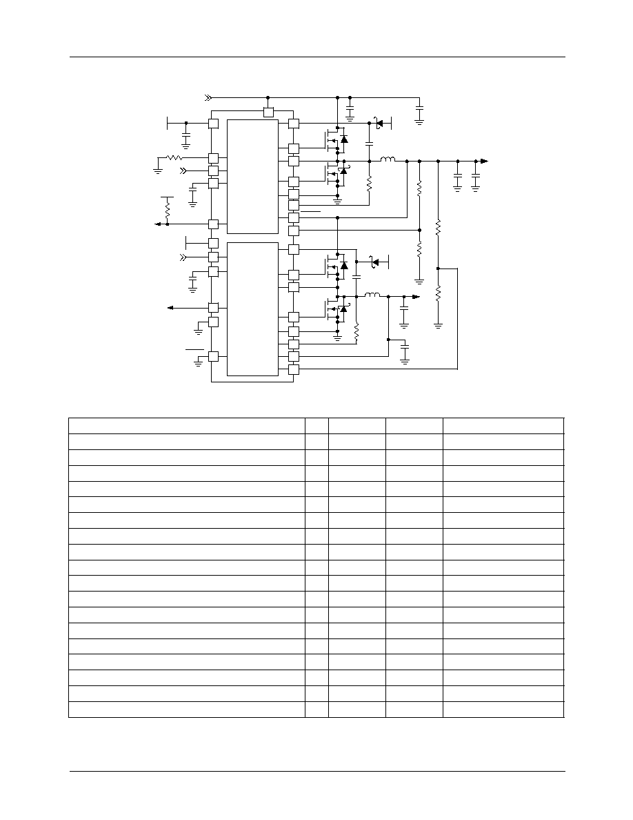
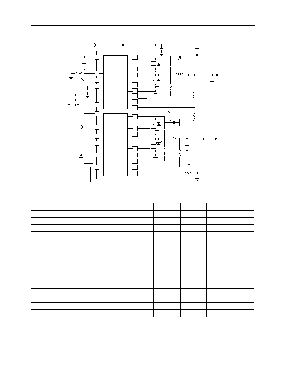
Generic Block Diagrams
Figure 1. Dual output regulator
Figure 2. Complete DDR Memory Power Supply
FAN5236
VIN (BATTERY)
= 5 to 24V
Q1
C
OUT1
VOUT1
= 2.5V
DDR
L
OUT1
Q2
C
OUT2
VOUT2
= 1.8V
L
OUT2
PWM 1
PWM 2
ILIM1
ILIM2/
REF2
VCC
+5
Q3
Q4
FAN5236
Q1
C
OUT1
VDDQ
= 2.5V
DDR
L
OUT1
Q2
C
OUT2
VTT =
VDDQ/2
L
OUT2
PWM 1
PWM 2
ILIM1
PG2/REF
R
R
VCC
+5
+5
ILIM2/REF2
VIN (BATTERY)
= 5 to 24V
Q3
Q4
1.25V

FAN5236
PRODUCT SPECIFICATION
REV. 1.1.7 4/4/03
3
Pin Configurations
Pin Definitions
Pin
Number
Pin Name
Pin Function Description
1
AGND
Analog Ground.
This is the signal ground reference for the IC. All voltage levels are
measured with respect to this pin.
2
27
LDRV1
LDRV2
Low-Side Drive.
The low-side (lower) MOSFET driver output. Connect to gate of low-side
MOSFET.
3
26
PGND1
PGND2
Power Ground.
The return for the low-side MOSFET driver. Connect to source of low-
side MOSFET.
4
25
SW1
SW2
Switching node.
Return for the high-side MOSFET driver and a current sense input.
Connect to source of high-side MOSFET and low-side MOSFET drain.
5
24
HDRV1
High-Side Drive.
High-side (upper) MOSFET driver output. Connect to gate of high-side
MOSFET.
6
23
BOOT1
BOOT2
BOOT.
Positive supply for the upper MOSFET driver. Connect as shown in Figure 3.
7
22
ISNS1
ISNS2
Current Sense input.
Monitors the voltage drop across the lower MOSFET or external
sense resistor for current feedback.
8
21
EN1
EN2
Enable
. Enables operation when pulled to logic high. Toggling EN will also reset the
regulator after a latched fault condition. These are CMOS inputs whose state is
indeterminate if left open.
9
20
FPWM1
FPWM2
Forced PWM mode.
When logic low, inhibits the regulator from entering hysteretic mode.
Otherwise tie to VOUT. The regulator uses VOUT on this pin to ensure a smooth
transition from Hysteretic mode to PWM mode. When VOUT is expected to exceed VCC,
tie to VCC.
10
19
VSEN1
VSEN2
Output Voltage Sense.
The feedback from the outputs. Used for regulation as well as
PG, under-voltage and over-voltage protection and monitoring.
11
ILIM1
Current Limit 1.
A resistor from this pin to GND sets the current limit.
12
17
SS1
SS2
Soft Start.
A capacitor from this pin to GND programs the slew rate of the converter
during initialization. During initialization, this pin is charged with a 5
µ
A current source.
13
DDR
DDR Mode Control.
High = DDR mode. Low = 2 separate regulators operating 180∞ out
of phase.
AGND
LDRV1
PGND1
SW1
HDRV1
BOOT1
ISNS1
EN1
FPWM1
VSEN1
ILIM1
SS1
DDR
VIN
FAN5236
1
2
3
4
5
6
7
8
9
10
11
12
13
14
28
27
26
25
24
23
22
21
20
19
18
17
16
15
VCC
LDRV2
PGND2
SW2
HDRV2
BOOT2
ISNS2
EN2
FPWM2
VSEN2
ILIM2/REF2
SS2
PG2/REF2OUT
PG1
QSOP-28 or TSSOP-28
JA
= 90
∞C/W
PRODUCT SPECIFICATION
FAN5236
4
REV. 1.1.7 4/4/03
Absolute Maximum Ratings
Absolute maximum ratings are the values beyond which the device may be damaged or have its useful life
impaired. Functional operation under these conditions is not implied.
Recommended Operating Conditions
Note 1: Industrial temperature range (≠40 to + 85∞C) may be special ordered from Fairchild. Please contact your authorized Fairchild
representative for more information.
14
VIN
Input Voltage.
Normally connected to battery, providing voltage feed-forward to set the
amplitude of the internal oscillator ramp. When using the IC for 2-step conversion from 5V
input, connect through 100K to ground, which will set the appropriate ramp gain and
synchronize the channels 90∞ out of phase.
15
PG1
Power Good Flag.
An open-drain output that will pull LOW when VSEN is outside of a
±10% range of the 0.9V reference.
16
PG2 /
REF2OUT
Power Good 2.
When not in DDR Mode: Open-drain output that pulls LOW when the
VOUT is out of regulation or in a fault condition
Reference Out 2.
When in DDR Mode, provides a buffered output of REF2. Typically
used as the VDDQ/2 reference.
18
ILIM2 /
REF2
Current Limit 2.
When not in DDR Mode, A resistor from this pin to GND sets the current
limit.
Reference
for reg #2 when in DDR Mode. Typically set to VOUT1 / 2.
28
VCC
VCC.
This pin powers the chip as well as the LDRV buffers. The IC starts to operate when
voltage on this pin exceeds 4.6V (UVLO rising) and shuts down when it drops below 4.3V
(UVLO falling).
Parameter
Min.
Typ.
Max.
Units
VCC Supply Voltage:
6.5
V
VIN
27
V
BOOT, SW, ISNS, HDRV
33
V
BOOTx to SWx
6.5
V
All Other Pins
≠0.3
VCC+0.3
V
Junction Temperature (T
J
)
≠40
150
∞C
Storage Temperature
≠65
150
∞C
Lead Soldering Temperature, 10 seconds
300
∞C
Parameter
Conditions
Min.
Typ.
Max.
Units
Supply Voltage VCC
4.75
5
5.25
V
Supply Voltage VIN
24
V
Ambient Temperature (T
A
)
Note 1
≠10
85
∞C
Pin Definitions
(continued)

FAN5236
PRODUCT SPECIFICATION
REV. 1.1.7 4/4/03
5
Electrical Specifications
Recommended operating conditions, unless otherwise noted.
Parameter
Conditions
Min.
Typ.
Max.
Units
Power Supplies
VCC Current
LDRV, HDRV Open, VSEN forced
above regulation point
2.2
3.0
mA
Shut-down (EN=0)
30
µ
A
VIN Current ≠ Sinking
VIN = 24V
10
30
µ
A
VIN Current ≠ Sourcing
VIN = 0V
≠15
≠30
µ
A
VIN Current ≠ Shut-down
1
µ
A
UVLO Threshold
Rising VCC
4.3
4.55
4.75
V
Falling
4.1
4.25
4.45
V
UVLO Hysteresis
300
mV
Oscillator
Frequency
255
300
345
KHz
Ramp Amplitude, pk≠pk
VIN = 16V
2
V
Ramp Amplitude, pk≠pk
VIN = 5V
1.25
V
Ramp Offset
0.5
V
Ramp / VIN Gain
VIN
3V
125
mV/V
Ramp / VIN Gain
1V < VIN < 3V
250
mV/V
Reference and Soft Start
Internal Reference Voltage
0.891
0.9
0.909
V
Soft Start current (I
SS
)
at start-up
5
µ
A
Soft Start Complete Threshold
1.5
V
PWM Converters
Load Regulation
I
OUTX
from 0 to 5A, VIN from 5 to 24V
-2
+2
%
VSEN Bias Current
50
80
120
nA
VOUT pin input impedance
45
55
65
K
Under-voltage Shutdown
as % of set point. 2
µ
S noise filter
70
75
80
%
Over-voltage threshold
as % of set point. 2
µ
S noise filter
115
120
125
%
I
SNS
Over-Current threshold
R
ILIM
= 68.5K
see Figure 11.
112
140
168
µ
A
Output Drivers
HDRV Output Resistance
Sourcing
12
15
Sinking
2.4
4
LDRV Output Resistance
Sourcing
12
15
Sinking
1.2
2
PG (Power Good Output) and Control pins
Lower Threshold
as % of set point, 2
µ
S noise filter
≠86
≠94
%
Upper Threshold
as % of set point, 2
µ
S noise filter
108
116
%
PG Output Low
IPG = 4mA
0.5
V
Leakage Current
V
PULLUP
= 5V
1
µ
A
PG2/REF2OUT Voltage
DDR = 1, 0 mA < I
REF2OUT
10mA
99
1.01
%
VREF2

PRODUCT SPECIFICATION
FAN5236
6
REV. 1.1.7 4/4/03
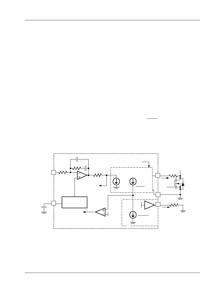
Figure 3. IC Block Diagram
DDR, EN Inputs
Input High
2
V
Input Low
0.8
V
FPWM Inputs
FPWM Low
0.1
V
FPWM High
FPWM connected to output
0.9
V
Electrical Specifications
Recommended operating conditions, unless otherwise noted.
(continued)
Parameter
Conditions
Min.
Typ.
Max.
Units
REF2
PGOOD
EN
C
BOOT
Q1
Q2
5V
VDD
ADAPTIVE
GATE
CONTROL LOGIC
CURRENT PROCESSING
HDRV
SW
LDRV
PGND
BOOT
VDD
HYST
ISNS
VIN
C
OUT
VOUT
PWM/HYST
PWM
S/H
ILIM
R
ILIM
R
SENSE
ILIM det.
HYST
SS
FPWM/VOUT
SS
DUTY
CYCLE
CLAMP
PWM
S
R
Q
RAMP
MODE
DDR
OSC
I
OU T
RAMP
CLK
OVP
POR/UVLO
Reference and
Soft Start
FPWM
L
OU T
VREF
EA
PWM/HYST
VSEN
FPWM/VOUT
VIN
DDR
DDR
FAN5236
PRODUCT SPECIFICATION
REV. 1.1.7 4/4/03
7
Typical Applications
Figure 4. DDR Regulator Application
Table 1. DDR Regulator BOM
Note 1
: Suitable for typical notebook computer application of 4A continuous, 6A peak for VDDQ. If continuous operation above
6A is required use single SO-8 packages for Q1A (FDS6612A) and Q1B (FDS6690S) respectively. Using FDS6690S,
change R7 to 1200
. Refer to Power MOSFET Selection, page 15 for more information.
Description
Qty
Ref.
Vendor
Part Number
Capacitor 68
µ
f, Tantalum, 25V, ESR 150m
1
C1
AVX
TPSV686*025#0150
Capacitor 10nf, Ceramic
2
C2, C3
Any
Capacitor 68
µ
f, Tantalum, 6V, ESR 1.8
1
C4
AVX
TAJB686*006
Capacitor 150nF, Ceramic
2
C5, C7
Any
Capacitor 180
µ
f, Specialty Polymer 4V, ESR 15m
2
C6A, C6B
Panasonic
EEFUE0G181R
Capacitor 1000
µ
f, Specialty Polymer 4V, ESR 10m
1
C8
Kemet
T510E108(1)004AS4115
Capacitor 0.1
µF, Ceramic
2
C9
Any
18.2K
, 1% Resistor
3
R1, R2
Any
1.82K
, 1% Resistor
1
R6
Any
56.2K
, 1% Resistor
2
R3
Any
10K
, 5% Resistor
2
R4
Any
3.24K
, 1% Resistor
1
R5
Any
1.5K
, 1% Resistor
2
R7, R8
Any
Schottky Diode 30V
2
D1, D2
Fairchild
BAT54
Inductor 6.4
µH, 6A, 8.64m
1
L1,
Panasonic
ETQ-P6F6R4HFA
Inductor 0.8
µH, 6A, 2.24m
1
L2
Panasonic
ETQ-P6F0R8LFA
Dual MOSFET with Schottky
1
Q1, Q2
Fairchild
FDS6986S (note 1)
DDR Controller
1
U1
Fairchild
FAN5236
FPWM1 (VOUT1)
2
C6A
VDDQ
= 2.5V
DDR
L1
Q1B
5
27
C8A
VTT =
VDDQ/2
L2
24
PWM 1
PWM 2
ILIM1
PG2/REF
14
13
11
16
R5
R6
18
28
VCC
+5
+5
ILIM2/REF2
Q2B
1.25V@10mA
C7
D1
+5
6
4
R7
7
25
R8
23
D2
+5
9
22
C4
19
VSEN2
ISNS2
1
AGND
R3
3
26
PGND2
SW2
HDRV2
ISNS1
PGND2
EN1
8
EN2
21
Q1A
Q2A
20
FPWM2
10
VSEN1
R2
R1
LDRV1
BOOT2
HDRV1
SW1
BOOT1
VIN
LDRV2
C5
C1
PG1
15
+5
R4
C9
VIN (BATTERY)
= 5 to 24V
SS1
12
C2
SS2
17
C3
C6B
C8B
PRODUCT SPECIFICATION
FAN5236
8
REV. 1.1.7 4/4/03
Typical Applications
(continued)
Figure 5. Dual Regulator Application
Table 2. Dual Regulator BOM
Note 1: If currents above 4A continuous required, use single SO-8 packages for Q1A/Q2A (FDS6612A) and Q1B/Q2B
(FDS6690S) respectively. Using FDS6690S, change R6/R7 as required. Refer to Power MOSFET Selection, page 15
for more information.
Item
Description
Qty
Ref.
Vendor
Part Number
1
Capacitor 68
µf, Tantalum, 25V, ESR 95m
1
C1
AVX
TPSV686*025#095
2
Capacitor 10nf, Ceramic
2
C2, C3
Any
3
Capacitor 68
µf, Tantalum, 6V, ESR 1.8
1
C4
AVX
TAJB686*006
4
Capacitor 150nF, Ceramic
2
C5, C7
Any
5
Capacitor 330
µf, Poscap, 4V, ESR 40m
2
C6, C8
Sanyo
4TPB330ML
5
Capacitor 0.1
µF, Ceramic
2
C9
Any
11
56.2K
, 1% Resistor
2
R1, R2
Any
12
10K
, 5% Resistor
2
R3
Any
13
3.24K
, 1% Resistor
1
R4
Any
14
1.82K
, 1% Resistor
3
R5, R8, R9
Any
15
1.5K
, 1% Resistor
2
R6, R7
Any
27
Schottky Diode 30V
2
D1, D2
Fairchild
BAT54
28
Inductor 6.4
µH, 6A, 8.64m
1
L1, L2
Panasonic
ETQ-P6F6R4HFA
29
Dual MOSFET with Schottky
1
Q1
Fairchild
FDS6986S (note 1)
30
DDR Controller
1
U1
Fairchild
FAN5236
FPWM1 (VOUT1)
2
C6
DDR
L1
Q1B
5
27
C8
1.8V@6A
L2
24
PWM 1
PWM 2
ILIM1
14
13
11
R4
R5
18
28
VCC
+5
ILIM2
Q2B
C7
D1
+5
6
4
R6
7
25
R7
23
D2
+5
9
22
C4
19
VSEN2
ISNS2
1
R2
PG1
15
+5
3
26
PGND2
SW2
HDRV2
ISNS1
PGND2
Q1A
Q2A
20
FPWM2
R8
R9
10
VSEN1
LDRV1
BOOT2
HDRV1
SW1
BOOT1
VIN
LDRV2
C5
C1
VIN
R1
2.5V@6A
PG2
16
EN2
21
R3
VIN (BATTERY)
= 5 to 24V
C9
SS2
17
C3
AGND
EN1
8
SS1
12
C2

FAN5236
PRODUCT SPECIFICATION
REV. 1.1.7 4/4/03
9
Circuit Description
Overview
The FAN5236 is a multi-mode, dual channel PWM control-
ler intended for graphic chipset, SDRAM, DDR DRAM or
other low voltage power applications in modern notebook,
desktop, and sub-notebook PCs. The IC integrates a control
circuitry for two synchronous buck converters. The output
voltage of each controller can be set in the range of 0.9V to
5.5V by an external resistor divider.
The two synchronous buck converters can operate from
either an unregulated DC source (such as a notebook battery)
with voltage ranging from 5.0V to 24V, or from a regulated
system rail of 3.3V to 5V. In either mode of operation the IC
is biased from a +5V source. The PWM modulators use an
average current mode control with input voltage feed-for-
ward for simplified feedback loop compensation and
improved line regulation. Both PWM controllers have inte-
grated feedback loop compensation that dramatically
reduces the number of external components.
Depending on the load level, the converters can operate
either in fixed frequency PWM mode or in a hysteretic mode.
Switch-over from PWM to hysteretic mode improves the
converters' efficiency at light loads and prolongs battery run
time. In hysteretic mode, comparators are synchronized to
the main clock that allows seamless transition between the
operational modes and reduced channel-to-channel interac-
tion. The hysteretic mode of operation can be inhibited inde-
pendently for each channel if variable frequency operation is
not desired.
The FAN5236 can be configured to operate as a complete
DDR solution. When the DDR pin is set high, the second
channel can provide the capability to track the output voltage
of the first channel. The PWM2 converter is prevented from
going into hysteretic mode if the DDR pin is set high. In
DDR mode, a buffered reference voltage (buffered voltage of
the REF2 pin), required by DDR memory chips, is provided
by the PG2 pin.
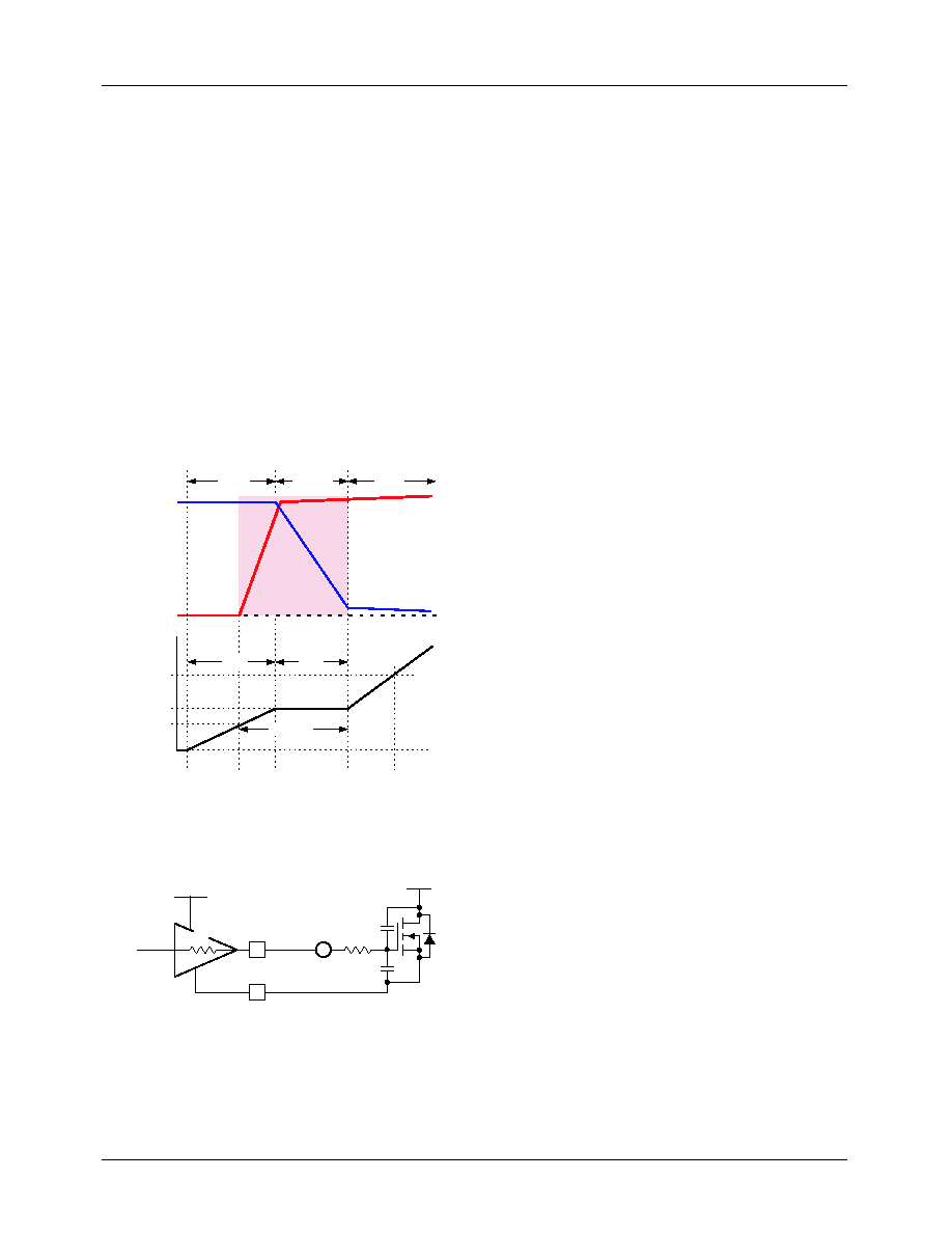
Converter Modes and Synchronization
Table 3. Converter modes and Synchronization
When used as a dual converter (as in Figure 5), out-of-phase
operation with 180 degree phase shift reduces input current
ripple.
For the "2-step" conversion (where the VTT is converted
from VDDQ as in Figure 4) used in DDR mode, the duty
cycle of the second converter is nominally 50% and the opti-
mal phasing depends on VIN. The objective is to keep noise
generated from the switching transition in one converter
from influencing the "decision" to switch in the other con-
verter.
When VIN is from the battery, it's typically higher than 7.5V.
As shown in Figure 6, 180∞ operation is undesirable since
the turn-on of the VDDQ converter occurs very near the
decision point of the VTT converter.
Figure 6. Noise-susceptible 180∞ phasing for DDR1
In-phase operation is optimal to reduce inter-converter inter-
ference when VIN is higher than 5V, (when VIN is from a
battery), as can be seen in Figure 7. Since the duty cycle
of PWM1 (generating VDDQ) is short, it's switching point
occurs far away from the decision point for the VTT
regulator, whose duty cycle is nominally 50%.
Figure 7. Optimal In-Phase operation for DDR1
When VIN
5V, 180∞ phase shifted operation can be
rejected for the same reasons demonstrated Figure 6.
In-phase operation with VIN
5V is even worse, since the
switch point of either converter occurs near the switch point
of the other converter as seen in Figure 8. In this case, as
VIN is a little higher than 5V it will tend to cause early
termination of the VTT pulse width. Conversely, VTT's
switch point can cause early termination of the VDDQ pulse
width when VIN is slightly lower than 5V.
Mode
VIN
VIN Pin
DDR
Pin
PWM 2 w.r.t.
PWM1
DDR1
Battery
VIN
HIGH
IN PHASE
DDR2
+5V
R to GND
HIGH
+ 90∞
DUAL
ANY
VIN
LOW
+ 180∞
VDDQ
VTT
CLK
VDDQ
VTT
CLK

PRODUCT SPECIFICATION
FAN5236
10
REV. 1.1.7 4/4/03
Figure 8. Noise-susceptible In-Phase operation for DDR2
These problems are nicely solved by delaying the 2
nd
con-
verter's clock by 90∞ as shown in Figure 9. In this way, all
switching transitions in one converter take place far away
from the decision points of the other converter.
Figure 9. Optimal 90∞ phasing for DDR2
Initialization and Soft Start
Assuming EN is high, FAN5236 is initialized when VCC
exceeds the rising UVLO threshold. Should VCC drop
below the UVLO threshold, an internal Power-On Reset
function disables the chip.
The voltage at the positive input of the error amplifier is lim-
ited by the voltage at the SS pin which is charged with a 5
µA
current source. Once C
SS
has charged to VREF (0.9V) the
output voltage will be in regulation. The time it takes SS to
reach 0.9V is:
where T
0.9
is in seconds if C
SS
is in
µF.
When SS reaches 1.5V, the Power Good outputs are enabled
and hysteretic mode is allowed. The converter is forced into
PWM mode during soft start.
Operation Mode Control
The mode-control circuit changes the converter's mode of
operation from PWM to Hysteretic and visa versa, based on
the voltage polarity of the SW node when the lower MOS-
FET is conducting and just before the upper MOSFET turns
on. For continuous inductor current, the SW node is negative
when the lower MOSFET is conducting and the converters
operate in fixed-frequency PWM mode as shown in Figure
10. This mode of operation achieves high efficiency at nomi-
nal load. When the load current decreases to the point where
the inductor current flows through the lower MOSFET in the
`reverse' direction, the SW node becomes positive, and the
mode is changed to hysteretic, which achieves higher effi-
ciency at low currents by decreasing the effective switching
frequency.
To prevent accidental mode change or "mode chatter" the
transition from PWM to Hysteretic mode occurs when the
SW node is positive for eight consecutive clock cycles (see
Figure 10). The polarity of the SW node is sampled at the
end of the lower MOSFET's conduction time. At the transi-
tion between PWM and hysteretic mode both the upper and
lower MOSFETs are turned off. The phase node will `ring'
based on the output inductor and the parasitic capacitance on
the phase node and settle out at the value of the output volt-
age.
The boundary value of inductor current, where current
becomes discontinuous, can be estimated by the following
expression.
VDDQ
VTT
CLK
VDDQ
VTT
CLK
T
0.9
0.9
C
SS
◊
5
-----------------------
=
(1)
I
LOAD DIS
(
)
V
IN
V
OUT
≠
(
)V
OUT
2F
SW
L
OUT
V
IN
--------------------------------------------------
=
(2)
Figure 10. Transitioning between PWM and Hysteretic Mode
PWM Mode
Hysteretic Mode
Hysteretic Mode
PWM Mode
1
2
3
4
5
6
7
8
V
CORE
I
L
0
V
CORE
I
L
0
1
2
3
4
5
6
7
8
FAN5236
PRODUCT SPECIFICATION
REV. 1.1.7 4/4/03
11
Hysteretic Mode
Conversely, the transition from Hysteretic mode to PWM
mode occurs when the SW node is negative for 8 consecutive
cycles.
A sudden increase in the output current will also cause a
change from hysteretic to PWM mode. This load increase
causes an instantaneous decrease in the output voltage due to
the voltage drop on the output capacitor ESR. If the load
causes the output voltage (as presented at VSNS) to drop
below the hysteretic regulation level (20mV below VREF),
the mode is changed to PWM on the next clock cycle.
In hysteretic mode, the PWM comparator and the error
amplifier that provide control in PWM mode are inhibited
and the hysteretic comparator is activated. In hysteretic
mode the low side MOSFET is operated as a synchronous
rectifier, where the voltage across ( V
DS(ON)
) it is monitored,
and it is switched off when V
DS(ON)
goes positive (current
flowing back from the load) allowing the diode to block
reverse conduction.
The hysteretic comparator initiates a PFM signal to turn on
HDRV at the rising edge of the next oscillator clock, when
the output voltage (at VSNS) falls below the lower threshold
(10mV below VREF) and terminates the PFM signal when
VSNS rises over the higher threshold (5mV above VREF).
The switching frequency is primarily a function of:
1.
Spread between the two hysteretic thresholds
2.
I
LOAD
3.
Output Inductor and Capacitor ESR
A transition back to PWM (Continuous Conduction Mode or
CCM) mode occurs when the inductor current rises suffi-
ciently to stay positive for 8 consecutive cycles. This occurs
when:
where
V
HYSTERESIS
= 15mV and ESR is the equivalent
series resistance of C
OUT
.
Because of the different control mechanisms, the value of the
load current where transition into CCM operation takes place
is typically higher compared to the load level at which transi-
tion into hysteretic mode occurs. Hysteretic mode can be
disabled by setting the FPWM pin low.
I
LOAD CCM
(
)
V
HYSTERESIS
2 ESR
---------------------------------------
=
(3)
Figure 11. Current Limit / Summing Circuits
LDRV
PGND
ISNS
in +
in Ò
2.5V
ILIM det.
R
SENSE
SS
1.5M
C
SS
VSEN
V to I
Reference and
Soft Start
17pf
I1B =
ISNS
9
I2 =
4 * ILIM
3
ILIM
0.9V
R
ILIM
ILIM mirror
S/H
TO PWM COMP
4.14K
300K
I1A =
ISNS
0.17pf
PRODUCT SPECIFICATION
FAN5236
12
REV. 1.1.7 4/4/03
Current Processing Section
The following discussion refers to Figure 11.
The current through R
SENSE
resistor (ISNS) is sampled
shortly after Q2 is turned on. That current is held, and
summed with the output of the error amplifier. This effec-
tively creates a current mode control loop. The resistor con-
nected to ISNSx pin (R
SENSE
) sets the gain in the current
feedback loop. For stable operation, the voltage induced by
the current feedback at the PWM comparator input should be
set to 30% of the ramp amplitude at maximum load currrent
and line voltage. The following expression estimates the
recommended value of R
SENSE
as a function of the maxi-
mum load current (I
LOAD(MAX)
) and the value of the
MOSFET's R
DS(ON)
:
R
SENSE
must, however, be kept higher than:
Setting the Current Limit
A ratio of ISNS is also compared to the current established
when a 0.9 V internal reference drives the ILIM pin. The
threshold is determined at the point
when the
. Since
therefore
,
Since the tolerance on the current limit is largely dependent
on the ratio of the external resistors it is fairly accurate if the
voltage drop on the Switching Node side of R
SENSE
is an
accurate representation of the load current. When using the
MOSFET as the sensing element, the variation of R
DS(ON)
causes proportional variation in the ISNS. This value not
only varies from device to device, but also has a typical junc-
tion temperature coefficient of about 0.4% / ∞C (consult the
MOSFET datasheet for actual values), so the actual current
limit set point will decrease propotional to increasing
MOSFET die temperature. A factor of 1.6 in the current
limit setpoint should compensate for all MOSFET R
DS(ON)
variations, assuming the MOSFET's heat sinking will keep
its operating die temperature below 125∞C.
Figure 12. Improving current sensing accuracy
More accurate sensing can be achieved by using a resistor
(R1) instead of the R
DS(ON)
of the FET as shown in Figure
12. This approach causes higher losses, but yields greater
accuracy in both V
DROOP
and I
LIMIT
. R1 is a low value
(e.g. 10m
) resistor.
Current limit (I
LIMIT
) should be set sufficiently high as to
allow inductor current to rise in response to an output load
transient. Typically, a factor of 1.3 is sufficient. In addition,
since I
LIMIT
is a peak current cut-off value, we will need to
multiply I
LOAD(MAX)
by the inductor ripple current (we'll
use 25%). For example, in Figure 5 the target for I
LIMIT
would be:
I
LIMIT
> 1.2
◊ 1.25 ◊ 1.6 ◊ 6A 14A
(6)
Duty Cycle Clamp
During severe load increase, the error amplifier output can
go to its upper limit pushing a duty cycle to almost 100% for
significant amount of time. This could cause a large increase
of the inductor current and lead to a long recovery from a
transient, over-current condition, or even to a failure espe-
cially at high input voltages. To prevent this, the output of
the error amplifier is clamped to a fixed value after two clock
cycles if severe output voltage excursion is detected, limiting
the maximum duty cycle to
This circuit is designed to not interfere with normal PWM
operation. When FPWM is grounded, the duty cycle clamp
is disabled and the maximum duty cycle is 87%.
Gate Driver section
The Adaptive gate control logic translates the internal PWM
control signal into the MOSFET gate drive signals providing
necessary amplification, level shifting and shoot-through
protection. Also, it has functions that help optimize the IC
performance over a wide range of operating conditions.
Since MOSFET switching time can vary dramatically from
type to type and with the input voltage, the gate control logic
provides adaptive dead time by monitoring the gate-to-
source voltages of both upper and lower MOSFETs.
R
SENSE
I
LOAD MAX
(
)
R
DS ON
(
)
4.1K
∑
∑
0.30
0.125
V
IN MAX
(
)
∑
∑
-----------------------------------------------------------------------------
100
≠
=
(4a)
R
SENSE MIN
(
)
I
LOAD MAX
(
)
R
DS ON
(
)
∑
150
µA
-----------------------------------------------------------
100
≠
=
(4b)
ISNS
9
--------------
ILIM
4
◊
3
-----------------------
>
ISNS
I
LOAD
R
DS ON
(
)
◊
100
R
+
SENSE
--------------------------------------------
=
I
LIMIT
0.9V
R
ILIM
---------------
4
3
---
◊
9
100
R
SENSE
+
(
)
◊
R
DS ON
(
)
-------------------------------------------------
◊
=
(5a)
or
R
ILIM
11.2
I
LIMIT
----------------
100
R
SENSE
+
(
)
R
DS ON
(
)
----------------------------------------
◊
=
(5b)
LDRV
PGND
ISNS
R
SENSE
R1
Q2
DC
MAX
V
OUT
V
IN
--------------
2.4
V
IN
---------
+
=

FAN5236
PRODUCT SPECIFICATION
REV. 1.1.7 4/4/03
13
The lower MOSFET drive is not turned on until the gate-to-
source voltage of the upper MOSFET has decreased to less
than approximately 1 volt. Similarly, the upper MOSFET is
not turned on until the gate-to-source voltage of the lower
MOSFET has decreased to less than approximately 1 volt.
This allows a wide variety of upper and lower MOSFETs to
be used without a concern for simultaneous conduction, or
shoot-through.
There must be a low-resistance, low-inductance path
between the driver pin and the MOSFET gate for the adap-
tive dead-time circuit to work properly. Any delay along that
path will subtract from the delay generated by the adaptive
dead-time circit and shoot-through may occur.
Frequency Loop Compensation
Due to the implemented current mode control, the modulator
has a single pole response with -1 slope at frequency deter-
mined by load
where R
O
is load resistance, C
O
is load capacitance.
For this type of modulator, Type 2 compensation circuit is
usually sufficient. To reduce the number of external compo-
nents and simplify the design task, the PWM controller has
an internally compensated error amplifier. Figure 13 shows a
Type 2 amplifier and its response along with the responses of
a current mode modulator and of the converter. The Type 2
amplifier, in addition to the pole at the origin, has a zero-pole
pair that causes a flat gain region at frequencies between the
zero and the pole.
This region is also associated with phase `bump' or reduced
phase shift. The amount of phase shift reduction depends the
width of the region of flat gain and has a maximum value of
90 degrees. To further simplify the converter compensation,
the modulator gain is kept independent of the input voltage
variation by providing feed-forward of VIN to the oscillator
ramp.
The zero frequency, the amplifier high frequency gain and
the modulator gain are chosen to satisfy most typical appli-
cations. The crossover frequency will appear at the point
where the modulator attenuation equals the amplifier high
frequency gain. The only task that the system designer has to
complete is to specify the output filter capacitors to position
the load main pole somewhere within one decade lower than
the amplifier zero frequency. With this type of compensation
plenty of phase margin is easily achieved due to zero-pole
pair phase `boost'.
Figure 13. Compensation
Conditional stability may occur only when the main load
pole is positioned too much to the left side on the frequency
axis due to excessive output filter capacitance. In this case,
the ESR zero placed within the 10kHz...50kHz range gives
some additional phase `boost'. Fortunately, there is an oppo-
site trend in mobile applications to keep the output capacitor
as small as possible.
If a larger inductor value or low ESR values are called for by
the application, additional phase margin can be achieved by
putting a zero at the LC crossover frequency. This can be
achieved with a capacitor across across the feedback resistor
(e.g. R5 from Figure 5) as shown below.
Figure 14. Improving Phase Margin
The optimal value of C(Z) is:
Protection
The converter output is monitored and protected against
extreme overload, short circuit, over-voltage and under-
voltage conditions.
A sustained overload on an output sets the PGx pin low and
latches-off the whole chip. Operation can be restored by
cycling the VCC voltage or by toggling the EN pin.
F
PO
1
2
R
O
C
O
----------------------
=
(7)
F
Z
1
2
R
2
C
1
--------------------
6kHz
=
=
(8a)
F
P
1
2
R
2
C
2
--------------------
600kHz
=
=
(8b)
R1
R2
EA Out
C1
C2
REF
V
IN
C
on
ve
rter
0
14
18
modulator
F
P0
F
Z
F
P
erro
r a
mp
C(OUT)
VOUT
C(Z)
R5
VSEN
L(OUT)
R6
C Z
( )
L OUT
(
) C OUT
(
)
◊
R5
------------------------------------------------------
=
(9)

PRODUCT SPECIFICATION
FAN5236
14
REV. 1.1.7 4/4/03
If VOUT drops below the under-voltage threshold, the chip
shuts down immediately.
Over-Current sensing
If the circuit's current limit signal ("ILIM det" as shown in
Figure 11) is high at the beginning of a clock cycle, a pulse-
skipping circuit is activated and HDRV is inhibited. The
circuit continues to pulse skip in this manner for the next 8
clock cycles. If at any time from the 9
th
to the 16
th
clock
cycle, the "ILIM det" is again reached, the over-current
protection latch is set, disabling the the chip. If "ILIM det"
does not occur between cycle 9 and 16, normal operation is
restored and the over-current circuit resets itself.
Figure 15. Over-Current protection waveforms
Over-Voltage / Under-voltage Protection
Should the VSNS voltage exceed 120% of VREF (0.9V) due
to an upper MOSFET failure, or for other reasons, the over-
voltage protection comparator will force LDRV high. This
action actively pulls down the output voltage and, in the
event of the upper MOSFET failure, will eventually blow the
battery fuse. As soon as the output voltage drops below the
threshold, the OVP comparator is disengaged.
This OVP scheme provides a `soft' crowbar function which
helps to tackle severe load transients and does not invert the
output voltage when activated -- a common problem for
latched OVP schemes.
Similarly, if an output short-circuit or severe load transient
causes the output to droop to less than 75% of its regulation
set point. Should this condition occur, the regulator will shut
down.
Over-Temperature Protection
The chip incorporates an over temperature protection circuit
that shuts the chip down when a die temperature of about
150∞C is reached. Normal operation is restored at die
temperature below 125∞C with internal Power On Reset
asserted, resulting in a full soft-start cycle.
Design and Component Selection
Guidelines
As an initial step, define operating input voltage range, out-
put voltage, minimum and maximum load currents for the
controller.
Setting the Output Voltage
The interal reference is 0.9V. The output is divided down by
a voltage divider to the VSEN pin (for example, R5 and R6
in Figure 4). The output voltage therefore is:
To minimize noise pickup on this node, keep the resistor to
GND (R6) below 2K. We selected R6 at 1.82K. Then choose
R5:
For DDR applications converting from 3.3V to 2.5V, or other
applications requiring high duty cycles, the duty cycle clamp
must be disabled by tying the converter's FPWM to GND.
When converter's FPWM is GND, the converter's maximum
duty cycle will be greater than 90%. When using as a DDR
converter with 3.3V input, set up the converter for In-Phase
synchronization by tying the VIN pin to +5V.
Output Inductor Selection
The minimum practical output inductor value is the one that
keeps inductor current just on the boundary of continuous
conduction at some minimum load. The industry standard
practice is to choose the minimum current somewhere from
15% to 35% of the nominal current. At light load, the
controller can automatically switch to hysteretic mode of
operation to sustain high efficiency. The following equations
help to choose the proper value of the output filter inductor.
where
I is the inductor ripple current and V
OUT
is the
maximum ripple allowed.
for this example we'll use:
V
IN
= 20V, V
OUT
= 2.5V
I = 20% * 6A = 1.2A
F
SW
= 300KHz.
therefore
L
6µH
1
2
3
CH1 5.0V
CH2 2.0A
CH2 100mV
M 10.0µs
IL
SHUTDOWN
PGOOD
8 CLK
VOUT
0.9V
R6
------------
V
OUT
0.9V
≠
R5
---------------------------------
=
(10a)
R5
1.82K
(
) V
OUT
0.9
≠
(
)
0.9
-----------------------------------------------------
3.24K
=
=
(10b)
I
2
I
MIN
◊
V
OUT
ESR
------------------
=
=
(11)
L
V
IN
V
OUT
≠
F
SW
I
◊
------------------------------
V
OUT
V
IN
--------------
◊
=
(12)

FAN5236
PRODUCT SPECIFICATION
REV. 1.1.7 4/4/03
15
Output Capacitor Selection
The output capacitor serves two major functions in a switch-
ing power supply. Along with the inductor it filters the
sequence of pulses produced by the switcher, and it supplies
the load transient currents. The output capacitor require-
ments are usually dictated by ESR, Inductor ripple current
(
I) and the allowable ripple voltage (V).
In addition, the capacitor's ESR must be low enough to allow
the converter to stay in regulation during a load step. The
ripple voltage due to ESR for the converter in Figure 5 is
120mV P-P. Some additional ripple will appear due to the
capacitance value itself:
which is only about 1.5mV for the converter in Figure 5 and
can be ignored.
The capacitor must also be rated to withstand the RMS
current which is approximately 0.3 X (
I), or about 400mA
for the converter in Figure 5. High frequency decoupling
capacitors should be placed as close to the loads as
physically possible.
Input Capacitor Selection
The input capacitor should be selected by its ripple current
rating.
Two-Stage Converter Case
In DDR mode (Figure 4), the VTT power input is powered
by the VDDQ output, therefore all of the input capacitor rip-
ple current is produced by the VDDQ converter. A conserva-
tive estimate of the output
current required for the 2.5V regulator is:
As an example, if average I
VDDQ
is 3A, and average I
VTT
is
1A, I
VDDQ
current will be about 3.5A. If average input volt-
age is 16V, RMS input ripple current will be:
where D is the duty cycle of the PWM1 converter:
therefore:
Dual Converter 180∞ phased
In Dual mode (Figure 5), both converters contribute to the
capacitor input ripple current. With each converter operating
180∞ out of phase, the RMS currents add in the following
fashion:
which for the dual 3A converters of Figure 5, calculates to:
Power MOSFET Selection
Losses in a MOSFET are the sum of its switching (P
SW
) and
conduction (P
COND
) losses.
In typical applications, the FAN5236 converter's output volt-
age is low with respect to its input voltage, therefore the
Lower MOSFET (Q2) is conducting the full load current for
most of the cycle. Q2 should therefore be selected to mini-
mize conduction losses, thereby selecting a MOSFET with
low R
DS(ON)
.
In contrast, the high-side MOSFET (Q1) has a much shorter
duty cycle, and it's conduction loss will therefore have less
of an impact. Q1, however, sees most of the switching losses,
so Q1's primary selection criteria should be gate charge.
High-Side Losses:
Figure 15 shows a MOSFET's switching interval, with the
upper graph being the voltage and current on the Drain to
Source and the lower graph detailing V
GS
vs. time with a
constant current charging the gate. The x-axis therefore is
also representative of gate charge (Q
G
) . C
ISS
= C
GD
+ C
GS
,
and it controls t1, t2, and t4 timing. C
GD
receives the current
from the gate driver during t3 (as V
DS
is falling). The gate
charge (Q
G
) parameters on the lower graph are either
specified or can be derived from MOSFET datasheets.
Assuming switching losses are about the same for both the
rising edge and falling edge, Q1's switching losses, occur
during the shaded time when the MOSFET has voltage
across it and current through it.
ESR
V
I
--------
<
(13)
V
I
C
OUT
8
◊
F
SW
◊
-----------------------------------------
=
(14)
I
REG1
I
VDDQ
I
VTT
2
------------
+
=
I
RMS
I
OUT MAX
(
)
D
D
2
≠
=
(15)
D
V
OUT
V
IN
--------------
<
2.5
16
-------
=
(16)
I
RMS
3.5
2.5
16
-------
2.5
16
-------
2
≠
1.49A
=
=
(17)
I
RMS
I
RMS 1
( )
2
I
RMS 2
( )
2
+
or
=
(18a)
I
RMS
I
1
( )
2
D
1
D
1
2
≠
(
)
I
2
( )
2
D
2
D
2
2
≠
(
)
+
=
(18b)
I
RMS
1.4A
=
PRODUCT SPECIFICATION
FAN5236
16
REV. 1.1.7 4/4/03
These losses are given by:
P
UPPER
= P
SW
+ P
COND
P
UPPER
is the upper MOSFET's total losses, and P
SW
and
P
COND
are the switching and conduction losses for a given
MOSFET. R
DS(ON)
is at the maximum junction temperature
(T
J
). t
S
is the switching period (rise or fall time) and is t2+t3
Figure 15.
The driver's impedance and C
ISS
determine t2 while t3's
period is controlled by the driver's impedance and Q
GD
.
Since most of t
S
occurs when V
GS
= V
SP
we can use a
constant current assumption for the driver to simplify the
calculation of t
S
:
Figure 16. Switching losses and Q
G
Figure 17. Drive Equivalent Circuit
Most MOSFET vendors specify Q
GD
and Q
GS
. Q
G(SW)
can
be determined as: Q
G(SW)
= Q
GD
+ Q
GS
≠ Q
TH
where Q
TH
is
the the gate charge required to get the MOSFET to it's
threshold (V
TH
). For the high-side MOSFET, V
DS
= VIN,
which can be as high as 20V in a typical portable applica-
tion. Care should also be taken to include the delivery of the
MOSFET's gate power (P
GATE
) in calculating the power
dissipation required for the FAN5236:
P
GATE
= Q
G
◊ VCC ◊ F
SW
(21)
where Q
G
is the total gate charge to reach VCC.
Low-Side Losses
Q2, however, switches on or off with its parallel shottky
diode conducting, therefore V
DS
0.5V. Since P
SW
is
proportional to V
DS
, Q2's switching losses are negligible
and we can select Q2 based on R
DS(ON)
only.
Conduction losses for Q2 are given by:
where R
DS(ON)
is the R
DS(ON)
of the MOSFET at the highest
operating junction temperature and
is the minimum duty cycle for the converter.
Since D
MIN
< 20% for portable computers, (1-D)
1
produces a conservative result, further simplifying the
calculation.
The maximum power dissipation (P
D(MAX)
) is a function of
the maximum allowable die temperature of the low-side
MOSFET, the
J-A
, and the maximum allowable ambient
temperature rise:
J-A
, depends primarily on the amount of PCB area that can
be devoted to heat sinking (see FSC app note AN-1029 for
SO-8 MOSFET thermal information).
P
SW
V
DS
I
L
◊
2
----------------------
2
◊
t
S
◊
F
SW
=
(19a)
P
COND
V
OUT
V
IN
--------------
I
OUT
2
◊
R
DS ON
(
)
◊
=
(19b)
V
SP
t1
t2
t3
4.5V
t4
t5
Q
G(SW)
V
DS
I
D
Q
GS
Q
GD
V
TH
V
GS
C
ISS
C
RSS
C
ISS
C
ISS
= C
GS
|| C
GD
C
GD
R
D
R
GATE
C
GS
HDRV
5V
SW
VIN
G
t
S
Q
G SW
(
)
I
DRIVER
---------------------
Q
G SW
(
)
VCC
V
SP
≠
R
DRIVER
R
GATE
+
-----------------------------------------------
-----------------------------------------------------
=
(20)
P
COND
1
D
≠
(
) I
OUT
2
◊
R
DS ON
(
)
◊
=
(22)
D
V
OUT
V
IN
--------------
=
P
D MAX
(
)
T
J MAX
(
)
T
A MAX
(
)
≠
J
A
≠
--------------------------------------------------
=
(23)

FAN5236
PRODUCT SPECIFICATION
REV. 1.1.7 4/4/03
17
Layout Considerations
Switching converters, even during normal operation,
produce short pulses of current which could cause substan-
tial ringing and be a source of EMI if layout constrains are
not observed.
There are two sets of critical components in a DC-DC
converter. The switching power components process large
amounts of energy at high rate and are noise generators. The
low power components responsible for bias and feedback
functions are sensitive to noise.
A multi-layer printed circuit board is recommended. Dedi-
cate one solid layer for a ground plane. Dedicate another
solid layer as a power plane and break this plane into smaller
islands of common voltage levels.
Notice all the nodes that are subjected to high dV/dt voltage
swing such as SW, HDRV and LDRV, for example. All
surrounding circuitry will tend to couple the signals from
these nodes through stray capacitance. Do not oversize
copper traces connected to these nodes. Do not place traces
connected to the feedback components adjacent to these
traces. It is not recommended to use High Density Intercon-
nect Systems, or micro-vias on these signals. The use of
blind or buried vias should be limited to the low current
signals only. The use of normal thermal vias is left to the
discretion of the designer.
Keep the wiring traces from the IC to the MOSFET gate and
source as short as possible and capable of handling peak
currents of 2A. Minimize the area within the gate-source
path to reduce stray inductance and eliminate parasitic ring-
ing at the gate.
Locate small critical components like the soft-start capacitor
and current sense resistors as close as possible to the respec-
tive pins of the IC.
The FAN5236 utilizes advanced packaging technologies
with lead pitches of 0.6mm. High performance analog semi-
conductors utilizing narrow lead spacing may require special
considerations in PWB design and manufacturing. It is
critical to maintain proper cleanliness of the area surround-
ing these devices. It is not recommended to use any type of
rosin or acid core solder, or the use of flux in either the
manufacturing or touch up process as these may contribute
to corrosion or enable electromigration and/or eddy currents
near the sensitive low current signals. When chemicals such
as these are used on or near the PWB, it is suggested that the
entire PWB be cleaned and dried completely before applying
power.

PRODUCT SPECIFICATION
FAN5236
18
REV. 1.1.7 4/4/03
Mechanical Dimensions
28-Pin QSOP
A
0.069
1.75
Symbol
Inches
Min.
Max.
Min.
Max.
Millimeters
Notes
A1
0.004
0.10
0.061
1.54
0.053
1.35
0.010
0.25
A2
-
-
B
0.008
0.012
0.20
0.30
D
0.386
0.394
9.81
10.00
H
0.150
0.157
3.81
3.98
0.016
0.050
0.41
1.27
E
0.025 BSC
0.635 BSC
e
h
L
0.228
0.244
0.0099
0.0196
5.80
6.19
0.26
0.49
0
∞
8
∞
0
∞
8
∞
6
5
7
9
3
4
N
28
28
C
0.007
0.010
0.18
0.25
Notes:
1.
2.
3.
4.
5.
6.
7.
8.
9.
10.
Symbols are defined in the "MO Series Symbol List" in
Section 2.2 of Publication Number 95.
Dimensioning and tolerancing per ANSI Y14.5M-1982.
Dimension "D" does not include mold flash, protrusions
or gate burrs. Mold flash, protrusions shall not exceed
0.25mm (0.010 inch) per side.
Dimension "E" does not include interlead flash or
protrusions. Interlead flash and protrusions shall not
exceed 0.25mm (0.010 inch) per side.
The chamber on the body is optional. If it is not present,
a visual index feature must be located within the
crosshatched area.
"L" is the length of terminal for soldering to a substrate.
"N" is the maximum number of terminals.
Terminal numbers are shown for reference only.
Dimension "B" does not include dambar protrusion.
Allowable dambar protrusion shall be 0.10mm (0.004
inch) total in excess of "B" dimension at maximum
material condition.
Controlling dimension: INCHES. Converted millimeter
dimensions are not necessarily exact.
H
E
A
A2
D
e
B
A1
≠ C ≠
ccc C
LEAD COPLANARITY
SEATING
PLANE
L
C

FAN5236
PRODUCT SPECIFICATION
REV. 1.1.7 4/4/03
19
Mechanical Dimensions
28-Pin TSSOP
9.7
± 0.1
15
≠ B ≠
0.1 C
PIN # 1 IDENT
14
ALL Lead Tips
0.2
LAND PATTERN RECOMMENDATION
0.65
0.42
B A
≠ A ≠
4.4
±
0.1
1.78
4.16
7.72
0.51 TYP
28
3.2
6.4
1.2 MAX
ALL LEAD TIPS
0.65
0.19≠0.30
0.13
0.90
See Detail A
0.09≠0.20
0.10
± 0.05
0
∞≠8∞
R0.31
R0.16
.025
GAGE PLANE
SEATING PLANE
DETAIL A
0.61
± 0.1
DIMENSIONS ARE IN MILLIMETERS
NOTES:
A. Conforms to JEDEC registration MO-153, variation AB,
Ref. Note 6, dated 7/93.
B. Dimensions are in millimeters.
C. Dimensions are exclusive of burrs, mold flash, and tie bar extensions.
D Dimensions and Tolerances per ANsI Y14.5M, 1982
1.00
12.00
∞ Top & Botom
+0.15
≠0.10
B
C
A
≠ C ≠

PRODUCT SPECIFICATION
FAN5236
LIFE SUPPORT POLICY
FAIRCHILD'S PRODUCTS ARE NOT AUTHORIZED FOR USE AS CRITICAL COMPONENTS IN LIFE SUPPORT DEVICES
OR SYSTEMS WITHOUT THE EXPRESS WRITTEN APPROVAL OF THE PRESIDENT OF FAIRCHILD SEMICONDUCTOR
CORPORATION. As used herein:
1. Life support devices or systems are devices or systems
which, (a) are intended for surgical implant into the body, or
(b) support or sustain life, and (c) whose failure to perform
when properly used in accordance with instructions for use
provided in the labeling, can be reasonably expected to
result in a significant injury of the user.
2. A critical component in any component of a life support
device or system whose failure to perform can be
reasonably expected to cause the failure of the life support
device or system, or to affect its safety or effectiveness.
www.fairchildsemi.com
4/4/03 0.0m 004
Stock#DS30005236
2002 Fairchild Semiconductor Corporation
Ordering Information
Part Number
Temperature Range
Package
Packing
FAN5236QSC
-10∞C to 85∞C
QSOP-28
Rails
FAN5236QSCX
-10∞C to 85∞C
QSOP-28
Tape and Reel
FAN5236MTC
-10∞C to 85∞C
TSSOP-28
Rails
FAN5236MTCX
-10∞C to 85∞C
TSSOP-28
Tape and Reel
DISCLAIMER
FAIRCHILD SEMICONDUCTOR RESERVES THE RIGHT TO MAKE CHANGES WITHOUT FURTHER NOTICE TO
ANY PRODUCTS HEREIN TO IMPROVE RELIABILITY, FUNCTION OR DESIGN. FAIRCHILD DOES NOT ASSUME
ANY LIABILITY ARISING OUT OF THE APPLICATION OR USE OF ANY PRODUCT OR CIRCUIT DESCRIBED HEREIN;
NEITHER DOES IT CONVEY ANY LICENSE UNDER ITS PATENT RIGHTS, NOR THE RIGHTS OF OTHERS.