 | –≠–ª–µ–∫—Ç—Ä–æ–Ω–Ω—ã–π –∫–æ–º–ø–æ–Ω–µ–Ω—Ç: FAN5616 | –°–∫–∞—á–∞—Ç—å:  PDF PDF  ZIP ZIP |

©2005 Fairchild Semiconductor Corporation
1
www.fairchildsemi.com
November 2005
FAN5616 Rev. 1.0.0
F
AN5616 High-Efficienc
y
,
Constant-Current LED Driver with Adaptive Char
g
e
Pump
FAN5616
High-Efficiency, Constant-Current LED Driver with
Adaptive Charge Pump
Features
3-Channel Parallel LED Driver for a Large Range of
Forward Voltages
Adaptive V
OUT
Adjustment to the Highest Diode
Forward Voltage
Internally Matched LED Current Sources
Matched LED Currents with Matched or Unmatched
LEDs
Built-in Charge Pump with Three Modes of Operation:
1x, 1.5x, and 2x
Up to 90% Efficiency
Up to 50kHz PWM Dimming Frequency
Low EMI, Low Ripple
Up to 120mA Output Current
Drives up to 3 LEDs at 40mA each
External Resistor to Set Maximum (100%) LED
Current
Built-in 2-bit DAC to Control LED Current in Digital
Mode
2.5V to 5.5V Input Voltage Range
I
CC
< 1µA in Shutdown Mode
1MHz Operating Frequency
Shutdown Isolates Output from Input
Smart Soft-Start Limits In-Rush Current
Short Circuit Protection
Minimal External Components Needed
Available in a 3x3mm 16-lead MLP Package
Applications
Cell Phones
PDAs, DSCs, and MP3 Players
Description
The FAN5616 generates a regulated output current from
a battery with an input voltage between 2.7V to 5.5V.
Switch reconfiguration and fractional switching tech-
niques are utilized to achieve high efficiency over the
entire input voltage range. The adaptive nature of the
built-in charge pump eliminates the need for LED pre-
selection (matching) and ensures operation with high
efficiency. The driver's built-in, proprietary, auto-sense
circuitry ensures the same high efficiency regardless of
the number of LEDs. When the input voltage is suffi-
ciently high to sustain the LED's programmed current
level, the FAN5616 reconfigures itself to operate as a lin-
ear regulator, and the charge pump is turned off.
The FAN5616 supports both digital and PWM LED
brightness control methods. The built-in 2-bit DAC offers
a selection of four LED current levels, each level is a per-
centage of the maximum LED current set by the external
R
SET
resistor.
The FAN5616 includes built-in shutdown, short circuit
and thermal protection circuitry. A built-in smart soft-start
circuitry prevents excessive current draw during power
on while allowing for an increased PWM frequency for
dimming.
Minimal external components are required. Only two
0.1µF to 1µF bucket capacitors, a 4.7µF input capacitor
and a 1µF output capacitor are needed for proper opera-
tion.
The FAN5616 is available in a 3x3mm 16-lead MLP
package.
Ordering Information
Product Number
Package Type
Order Code
FAN5616
3x3mm 16-Lead MLP
FAN5616MPX
2
www.fairchildsemi.com
FAN5616 Rev. 1.0.0
F
AN5616 High-Efficienc
y
,
Constant-Current LED Driver with Adaptive Char
g
e
Pump
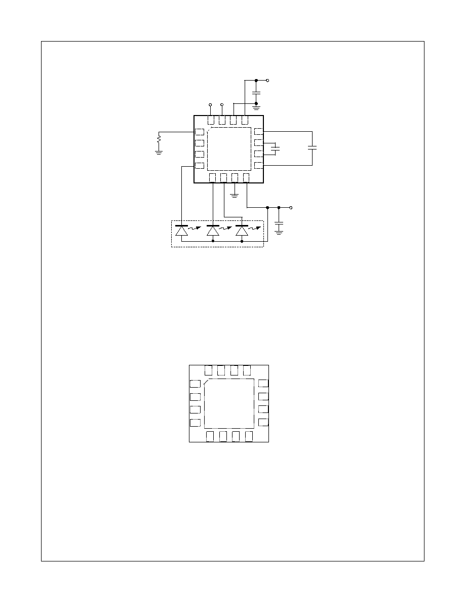
Typical Application
Figure 1. Typical Application
Pin Assignment
Figure 2. Pin Assignment
V
IN
C
IN
V
OUT
C
OUT
EN1
EN2
CAP1
NC
GND
CAP2
R
SET
NC
1
2
3
4
5
6
7
8
9
10
11
12
13
14
15
16
P1
(GND)
Top View
CAP1+
CAP1-
NC
GND
V
IN
V
OUT
LED-
LED-
PGND
LED-
CAP2-
CAP2+
EN1
EN2
R
SET
NC
1
2
3
4
5
6
7
8
9
10
11
12
13
14
15
16
P1
(GND)
3x3mm 16-Lead MLP

3
www.fairchildsemi.com
FAN5616 Rev. 1.0.0
F
AN5616 High-Efficienc
y
,
Constant-Current LED Driver with Adaptive Char
g
e
Pump
Pin Description
Pin No.
Pin Name
Pin Description
P1
GND
Ground.
P1 must be soldered to the PCB ground.
1
R
SET
R
SET
Pin.
Connect this pin to the resistor used to set the maximum LED current.
2
NC
No Connection.
3
NC
No Connection.
4
LED-
1st LED Cathode.
Connect this pin to the LED's cathode.
5
LED-
2nd LED Cathode.
Connect this pin to the LED's cathode.
6
LED-
3rd LED Cathode.
Connect this pin to the LED's cathode.
7
PGND
Power Ground.
8
V
OUT
Output Voltage.
Connect this pin to all of the LED's anodes.
9
CAP2+
Bucket Capacitor 2.
Connect this pin to the positive terminal of the bucket capacitor.
10
CAP1+
Bucket Capacitor 1.
Connect this pin to the positive terminal of the bucket capacitor.
11
CAP1-
Bucket Capacitor 1.
Connect this pin to the negative terminal of the bucket capacitor.
12
CAP2-
Bucket Capacitor 2.
Connect this pin to the negative terminal of the bucket capacitor.
13
V
IN
Supply Voltage Input.
14
GND
Ground.
15
EN1
Enable Input.
16
EN2
Enable Input.
4
www.fairchildsemi.com
FAN5616 Rev. 1.0.0
F
AN5616 High-Efficienc
y
,
Constant-Current LED Driver with Adaptive Char
g
e
Pump
Absolute Maximum Ratings
(Note1)
Recommended Operating Conditions
Notes:
1. Stresses above those listed under "Absolute Maximum Ratings" may cause permanent damage to the device. This
is a stress rating only and functional operation of the device at these or any other conditions above those indicated
in the operational section of this specification is not implied. Exposure to absolute maximum rating conditions for
extended periods may affect device reliability. Absolute maximum ratings apply individually only, not in combination.
Unless otherwise specified all other voltages are referenced to GND.
2. Junction to ambient thermal resistance,
JA
, is a strong function of PCB material, board thickness, thickness
and number of via used, diameter of via used, available copper surface, and attached heat sink characteristics.
A reasonable estimated value for
JA
for zero air flow at 0.5W is 60∞C/W.
3. Using Mil Std. 883E, method 3015.7(Human Body Model) and EIA/JESD22C101-A (Charge Device Model).
Parameter
Min
Max
Unit
V
IN
, V
OUT
, EN1, EN2, GND
-0.3
6
V
Voltage On All Other Pins
GND ≠ 0.3
V
IN
+ 0.3
V
CAP+, CAP- to GND
-0.3
V
IN
+ 0.3
V
Thermal Resistance ≠ Junction to Tab (
JC
) (Note 2)
8
∞C/W
Lead Soldering Temperature (10 seconds)
260
∞C
Junction Temperature
150
∞C
Storage Temperature
-65
150
∞C
Electrostatic Discharge Protection (ESD) Level (Note 3)
HBM
2.5
kV
CDM
1.5
Parameter
Min
Max
Unit
Supply Voltage Range
2.5
5.5
V
LED Forward Voltage
4
V
Current Through Each LED
2
40
mA
PWM Dimming Signal Frequency
0.2
50
kHz
Operating Ambient Temperature
-40
+85
∞C
Operating Junction Temperature
-40
+125
∞C

5
www.fairchildsemi.com
FAN5616 Rev. 1.0.0
F
AN5616 High-Efficienc
y
,
Constant-Current LED Driver with Adaptive Char
g
e
Pump
Electrical Characteristics
Unless otherwise noted, V
IN
= 2.7V to 5.5V, I
LED
= 2mA to 20mA, EN1 = EN2 = HIGH, T
A
= -40∞C to +85∞C. Typical
values are at 25∞C.
Notes:
1. Current Matching refers to the absolute value of the difference in the current between the two LED branches.
2. Efficiency is expressed as a ratio between the electrical power into the LEDs and the total power consumed from
the input power supply.
Some competitors calculate the efficiency as a function of V
OUT
instead of LED V
F
. Their method does not account
for the power lost due to the cathode voltage not being equal to zero. This method allows them to provide an
"improved" efficiency up to 5%.
Parameter
Conditions
Min
Typ
Max
Unit
Input Under-Voltage Lockout
V
IN
falling
1.6
V
V
IN
rising
2.3
I
LED
/I
SET
Ratio
V
IN
= 3.6V, I
OUT
= 15mA
240
255
270
I
LED
/I
SET
Ratio
I
LED
= 2 to 20mA
230
260
280
I
LED
/I
SET
Ratio
EN1 = HIGH, EN2 = LOW
86
EN1 = LOW, EN2 = HIGH
173
Current Matching with Unmatched
LEDs (Note 1)
2mA
I
LED
15mA
2.8V
LED V
F
<4V
0.6
+3
%
Reference Voltage for Current Set
588
600
612
mV
Start Up time
C
OUT
= 1µF, V
IN
= 3.6V,
I
LED
= 15mA
200
270
500
µS
Minimum Cathode Voltage
I
LED
= 15mA
170
250
mV
Quiescent Current
V
IN
= 5.5V, I
OUT
= 5mA
250
µA
Shutdown Supply Current
EN1 = EN2 = Logic "L"
0.1
1
µA
Output Short Circuit Current
V
IN
= 5.5V, V
OUT
= 0V
65
80
mA
V
OUT
Over-voltage Protection
6
V
V
IN
at Mode Transition from 1x to 1.5x
LED V
f
= 3.5V, I
LED
= 3 x 20mA
3.9
V
V
IN
at Mode Transition from 1.5x to 2x
LED V
f
= 3.5V, I
LED
= 3 x 20mA
2.9
V
Peak Efficiency (Note 2)
V
IN
= 3.75V, LED V
f
= 3.4V,
I
LED
= 18mA
90
%
Oscillator Frequency
0.8
1
1.2
MHz
Thermal Shutdown Threshold
150
∞C
Thermal Shutdown Hysteresis
15
∞C
"EN1" Logic Input Low Voltage
0.4
V
"EN1" Logic Input High Voltage
1.6
V
"EN2" Logic Input Low Voltage
0.4
V
"EN2" Logic Input High Voltage
1.6
V
(
(
)
)
LEDj
LEDi
LEDj
LEDi
I
I
100
x
I
I
Current Matching (%)
+
, where i, j = 1, 2 or 3
≠
≠
≠
≠
IN
IN
3
1
i
LEDi
LEDi
I
x
V
I
x
V
Efficiency
=
≠
≠
≠