 | –≠–ª–µ–∫—Ç—Ä–æ–Ω–Ω—ã–π –∫–æ–º–ø–æ–Ω–µ–Ω—Ç: H11F3 | –°–∫–∞—á–∞—Ç—å:  PDF PDF  ZIP ZIP |
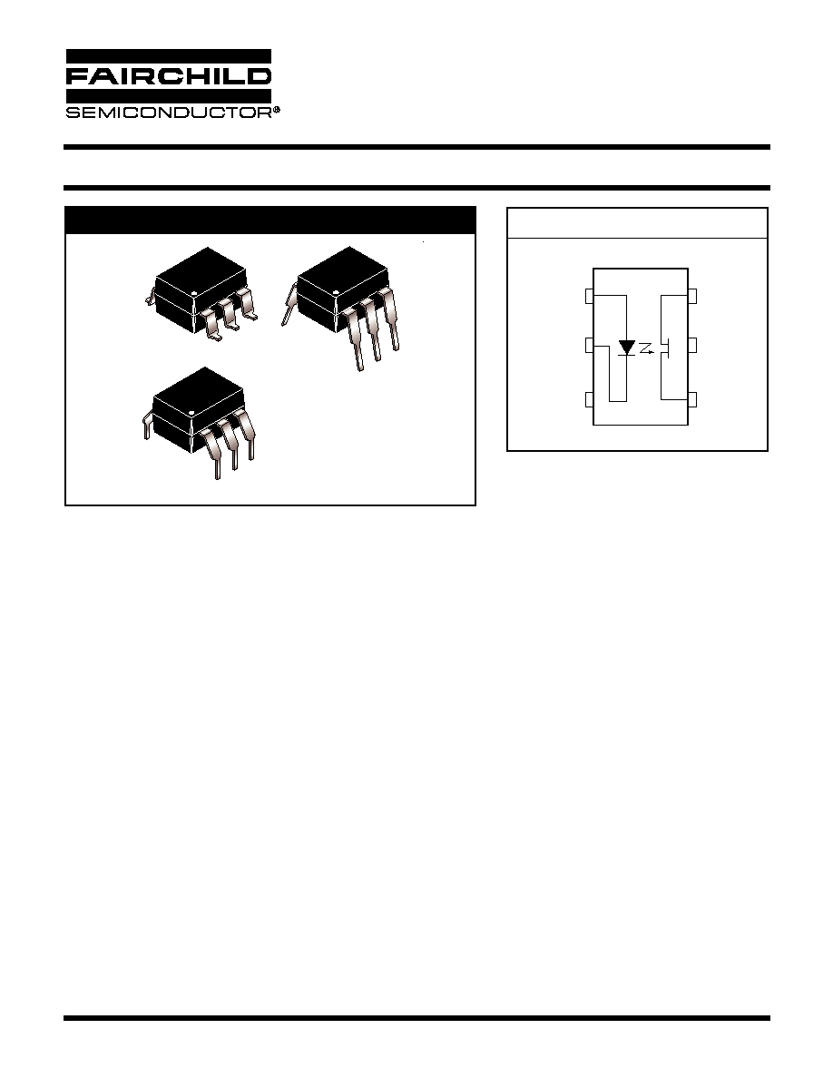
PACKAGE
SCHEMATIC
PHOTO FET OPTOCOUPLERS
6/24/02
Page 1 of 9
© 2002 Fairchild Semiconductor Corporation
H11F1 H11F2 H11F3
DESCRIPTION
The H11F series consists of a Gallium-Aluminum-Arsenide IRED emitting diode coupled to a symmetrical bilateral silicon photo-
detector. The detector is electrically isolated from the input and performs like an ideal isolated FET designed for distortion-free
control of low level AC and DC analog signals. The H11F series devices are mounted in dual in-line packages.
FEATURES
As a remote variable resistor
∑
100
to
300 M
∑
99.9% linearity
∑
15 pF shunt capacitance
∑
100 G
I/O isolation resistance
As an analog switch
∑
Extremely low offset voltage
∑
60 V
pk-pk
signal capability
∑
No charge injection or latch-up
∑
t
on
, t
off
15 µS
∑
UL recognized (File #E90700)
∑
VDE recognized (File #E94766)
≠ Ordering option `300' (e.g. H11F1.300)
APPLICATIONS
As a variable resistor ≠
∑
Isolated variable attenuator
∑
Automatic gain control
∑
Active filter fine tuning/band switching
As an analog switch ≠
∑
Isolated sample and hold circuit
∑
Multiplexed, optically isolated A/D conversion
6
1
6
1
6
1
1
2
6
5
4
OUTPUT
TERM.
OUTPUT
TERM.
ANODE
CATHODE
3

6/24/02
Page 2 of 9
© 2002 Fairchild Semiconductor Corporation
PHOTO FET OPTOCOUPLERS
H11F1 H11F2 H11F3
Absolute Maximum Ratings
(T
A
= 25∞C unless otherwise specified)
Parameter
Symbol
Device
Value
Units
TOTAL DEVICE
Storage Temperature
T
STG
All
-55 to +150
∞C
Operating Temperature
T
OPR
All
-55 to +100
∞C
Lead Solder Temperature
T
SOL
All
260 for 10 sec
∞C
EMITTER
Continuous Forward Current
I
F
All
60
mA
Reverse Voltage
V
R
All
5
V
Forward Current - Peak (10 µs pulse, 1% duty cycle)
I
F(pk)
All
1
A
LED Power Dissipation 25∞C Ambient
P
D
All
100
mW
Derate Linearly From 25∞C
1.33
mW/∞C
DETECTOR
Detector Power Dissipation @ 25∞C
P
D
All
300
mW
Derate linearly from 25∞C
4.0
mW/∞C
Breakdown Voltage (either polarity)
BV
4-6
H11F1, H11F2
±30
V
H11F3
±15
V
Continuous Detector Current (either polarity)
I
4-6
All
±100
mA
ELECTRICAL CHARACTERISTICS
(T
A
= 25∞C Unless otherwise specified.)
INDIVIDUAL COMPONENT CHARACTERISTICS
Parameter
Test Conditions
Symbol
Device
Min
Typ*
Max
Unit
EMITTER
Input Forward Voltage
I
F
= 16 mA
V
F
All
1.3
1.75
V
Reverse Leakage Current
V
R
= 5 V
I
R
All
10
µA
Capacitance
V = 0 V, f = 1.0 MHz
C
J
All
50
pF
OUTPUT DETECTOR
Breakdown Voltage
Either Polarity
I
4-6
= 10µA, I
F
= 0
BV
4-6
H11F1, H11F2
30
V
H11F3
15
Off-State Dark Current
V
4-6
= 15 V, I
F
= 0
I
4-6
All
50
nA
V
4-6
= 15 V, I
F
= 0, T
A
= 100∞C
All
50
µA
Off-State Resistance
V
4-6
= 15 V, I
F
= 0
R
4-6
All
300
M
Capacitance
V
4-6
= 15 V, I
F
= 0, f = 1MHz
C
4-6
All
15
pF
6/24/02
Page 3 of 9
© 2002 Fairchild Semiconductor Corporation
PHOTO FET OPTOCOUPLERS
H11F1 H11F2 H11F3
ISOLATION CHARACTERISTICS
Parameter
Test Conditions
Symbol
Min
Typ*
Max
Units
Input-Output Isolation Voltage
f = 60Hz, t = 1 min.
V
ISO
5300
Vac (rms)
Isolation Resistance
V
I-O
= 500 VDC
R
ISO
10
11
Isolation Capacitance
V
I-O
= 0, f = 1.0 MHz
C
ISO
2
pF
TRANSFER CHARACTERISTICS
(T
A
= 25∞C Unless otherwise specified.)
DC Characteristics
Test Conditions
Symbol
Device
Min
Typ*
Max
Units
On-State Resistance
I
F
= 16 mA, I
4-6
= 100 µA
R
4-6
H11F1
200
H11F2
330
H11F3
470
On-State Resistance
I
F
= 16 mA, I
6-4
= 100 µA
R
6-4
H11F1
200
H11F2
330
H11F3
470
Resistance, non-linearity
and assymetry
I
F
= 16mA, I
4-6
= 25 µA RMS,
f = 1kHz
All
0.1
%
AC Characteristics
Test Conditions
Symbol
Device
Min
Typ*
Max
Units
Turn-On Time
R
L
= 50
, I
F
= 16mA, V
4-6
= 5V
t
on
All
25
µS
Turn-Off Time
R
L
= 50
, I
F
= 16mA, V
4-6
= 5V
t
off
All
25
µS
6/24/02
Page 4 of 9
© 2002 Fairchild Semiconductor Corporation
PHOTO FET OPTOCOUPLERS
H11F1 H11F2 H11F3
3
1
2
0.8
0.6
0.4
-25
-50
0
25
50
75
100
T
A
- AMBIENT TEMPERATURE - ∞C
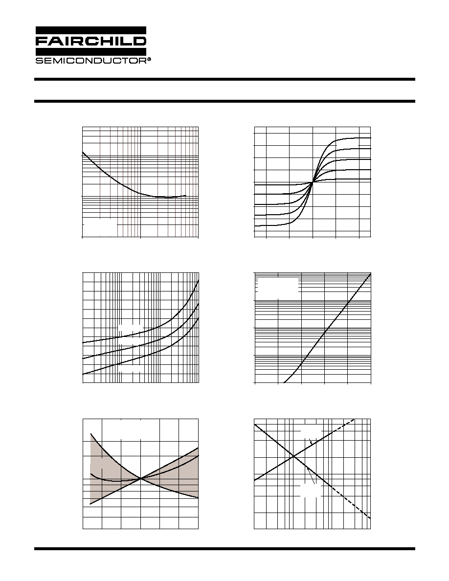
Figure 5. Resistance vs. Temperature
r(on) - NORMALIZED RESIST
ANCE
2
1
8
6
4
40
20
10
100
80
60
2
8
6
4
40
20
10
100
80
60
100
1000
10K
100K
r(on) RESISTANCE -
Figure 6. Region of Linear Resistance
V
4-6
- MAXIMUM RMS SIGNAL
V
O
L
T
A
GE - mV
I 4-6
- MAXIMUM RMS SIGNAL CURRENT -
µ
A
1K
MAXIMUM
RMS
VOLTAGE
MAXIMUM
RMS
CURRENT
10000
1000
100
10
1
0
20
40
60
T
A
- AMBIENT TEMPERATURE (
∞C)
Figure 4. Off-state Current vs. Ambient Temperature
I
46
- NORMALIZED DARK CURRENT
80
100
NORMALIZED TO:
V
46
= 15V
I
F
= 0mA
T
A
= 25
∞C
800
600
400
200
0
-200
-400
-600
-800
-0.2
-0.1
0.0
I
F
= 2mA
I
F
= 2mA
I
F
= 6mA
I
F
= 6mA
I
F
= 10mA
I
F
= 10mA
I
F
= 14mA
I
F
= 14mA
I
F
= 18mA
I
F
= 18mA
0.1
0.2
V
46
- OUTPUT VOLTAGE (V)
I
46
- OUTPUT CURRENT (
µ
A)
Figure 2. Output Characteristics
10
1
10
100
I
F
- INPUT CURRENT - mA
r(on) - Nor
maliz
ed Resistance
Figure 1. Resistance vs. Input Current
1
0.1
Normalized to:
I
F
= 16 mA
I
46
= 5
µA RMS
Figure 3. LED Forward Voltage vs. Forward Current
2.0
1.8
1.6
1.4
1.2
1.0
0.1
10
1
100
I
F
- LED FORWARD CURRENT - mA
V
F
- FOR
W
ARD
V
O
L
T
A
GE (V)
0.8
T
A
= -55
∞C
T
A
= 25
∞C
T
A
= 100
∞C
NORMALIZED TO
I
F
= 16mA
I
4-6
= 25
µA RMS
T
A
= 25∞C
Observed
Range
Median
De
vice

6/24/02
Page 5 of 9
© 2002 Fairchild Semiconductor Corporation
PHOTO FET OPTOCOUPLERS
H11F1 H11F2 H11F3
5
3
2
1
1
50
100
150
200
250
300
350
V
4-6
- D.C. BIAS VOLTAGE - mA
r(on) - CHANGE IN RESIST
ANCE
≠
%
Figure 7. Resistive non-linearity vs. D.C. Bias
4
0
I
4-6
= 10
µA RMS
r(on) = 200
6/24/02
Page 6 of 9
© 2002 Fairchild Semiconductor Corporation
PHOTO FET OPTOCOUPLERS
H11F1 H11F2 H11F3
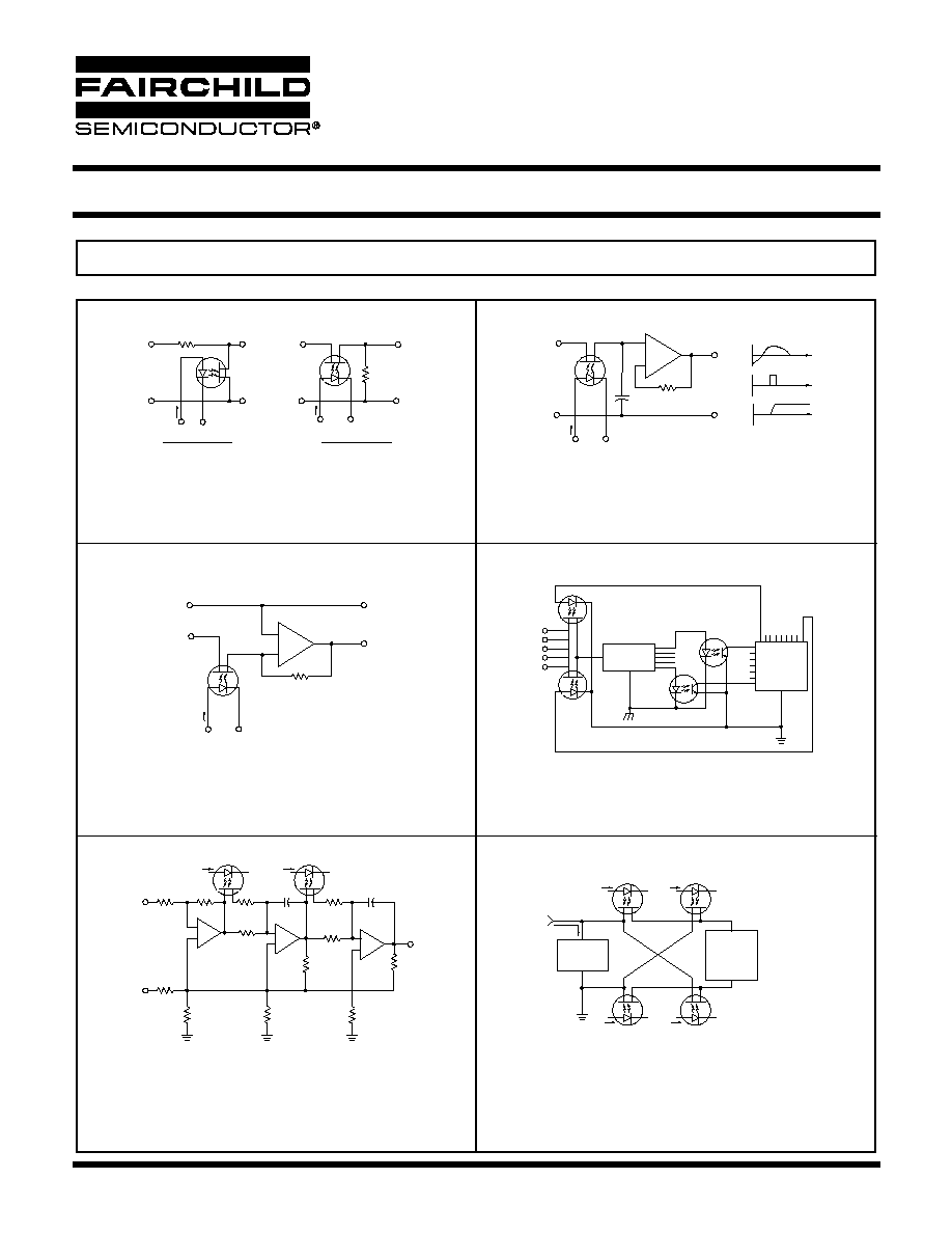
TYPICAL APPLICATIONS
AS A VARIABLE RESISTOR
AS AN ANALOG SIGNAL SWITCH
ISOLATED VARIABLE ATTENUATORS
Distortion free attenuation of low level A.C. signals is accom-
plished by varying the IRED current, I
F
Note the wide dynamic
range and absence of coupling capacitors; D.C. level shifting or
parasitic feedback to the controlling function.
ISOLATED SAMPLE AND HOLD CIRCUIT
Accuracy and range are improved over conventional FET
switches because the H11F has no charge injection from the
control signal. The H11F also provides switching of either
polarity input signal up to 30V magnitude.
AUTOMATIC GAIN CONTROL
This simple circuit provides over 70db of stable gain control for
an AGC signal range of from 0 to 30mA. This basic circuit can
be used to provide programmable fade and attack for electronic
music.
MULTIPLEXED, OPTICALLY-ISOLATED A/D CONVERSION
The optical isolation, linearity and low offset voltage of the
H11F allows the remote multiplexing of low level analog signals
from such transducers as thermocouplers, Hall effect devices,
strain gauges, etc. to a single A/D converter.
ACTIVE FILTER FINE TUNING/BAND SWITCHING
The linearity of resistance and the low offset voltage of the
H11F allows the remote tuning or band-switching of active
filters without switching glitches or distortion. This schematic
illustrates the concept, with current to the H11F1 IRED's
controlling the filter's transfer characteristic.
TEST EQUIPMENT - KELVIN CONTACT POLARITY
In many test equipment designs the auto polarity function uses
reed relay contacts to switch the Kelvin Contact polarity. These
reeds are normally one of the highest maintenance cost items
due to sticking contacts and mechanical problems. The totally
solid-State H11F eliminates these troubles while providing
faster switching.
500K
V
IN
V
OUT
V
IN
V
OUT
500K
50
I
F
H11F1
I
F
H11F1
LOW FREQUENCY
HIGH FREQUENCY
DYNAMIC RANGE
70db
FOR 0
I
F
30mA
@10KHz
DYNAMIC RANGE
50db
FOR 0
I
F
30mA
@1MHz
V
IN
V
OUT
I
F
V
IN
V
OUT
I
F
t
H11F1
C
+
-
V
IN
V
OUT
I
F
H11F1
AGC
SIGNAL
500K
+
-
V
1
CALL V1
V
2
V
n
H11F1
MSB
MSB
CALL
V
n
D
ATA
INPUT
H11F1
LSB
LSB
H74A1
H74A1
A/D
CONVERTER
PROCESS
CONTROL
LOGIC
SYSTEM
DATA
ACQUISITION
I
F1
ADJUSTS f
1
, I
F2
ADJUSTS f
2
I
F1
A2
A3
A1
H11F1
I
F2
H11F1
I
F
A
C
H11F1
I
F
H11F1
I
F
I
TEST
B
D
H11F1
I
F
H11F1
DEVICE
UNDER
TEST
PARAMETER
SENSING
BOARD
I
F
TO
A & B FOR
POLARITY 1
C & D FOR
POLARITY 2
6/24/02
Page 7 of 9
© 2002 Fairchild Semiconductor Corporation
PHOTO FET OPTOCOUPLERS
H11F1 H11F2 H11F3
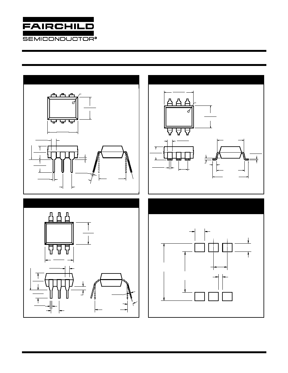
NOTE
All dimensions are in inches (millimeters)
Package Dimensions (Through Hole)
Package Dimensions (Surface Mount)
Package Dimensions (0.4" Lead Spacing)
Recommended Pad Layout for
Surface Mount Leadform
0.100 (2.54)
TYP
0.020 (0.51)
MIN
0.350 (8.89)
0.330 (8.38)
0.270 (6.86)
0.240 (6.10)
PIN 1
ID.
0.022 (0.56)
0.016 (0.41)
0.070 (1.78)
0.045 (1.14)
0.200 (5.08)
0.135 (3.43)
0.300 (7.62)
TYP
0
∞ to 15∞
0.154 (3.90)
0.100 (2.54)
SEATING PLANE
0.016 (0.40)
0.008 (0.20)
Lead Coplanarity : 0.004 (0.10) MAX
0.270 (6.86)
0.240 (6.10)
0.350 (8.89)
0.330 (8.38)
0.300 (7.62)
TYP
0.405 (10.30)
MAX
0.315 (8.00)
MIN
0.016 (0.40) MIN
2
5
PIN 1
ID.
0.016 (0.41)
0.008 (0.20)
0.100 (2.54)
TYP
0.022 (0.56)
0.016 (0.41)
0.070 (1.78)
0.045 (1.14)
0.200 (5.08)
0.165 (4.18)
4
3
0.020 (0.51)
MIN
1
6
SEATING PLANE
0.016 (0.40)
0.008 (0.20)
0.070 (1.78)
0.045 (1.14)
0.350 (8.89)
0.330 (8.38)
0.154 (3.90)
0.100 (2.54)
0.200 (5.08)
0.135 (3.43)
0.004 (0.10)
MIN
0.270 (6.86)
0.240 (6.10)
0.400 (10.16)
TYP
0∞ to 15∞
0.022 (0.56)
0.016 (0.41)
0.100 (2.54) TYP
0.070 (1.78)
0.060 (1.52)
0.030 (0.76)
0.100 (2.54)
0.295 (7.49)
0.415 (10.54)
6/24/02
Page 8 of 9
© 2002 Fairchild Semiconductor Corporation
PHOTO FET OPTOCOUPLERS
H11F1 H11F2 H11F3
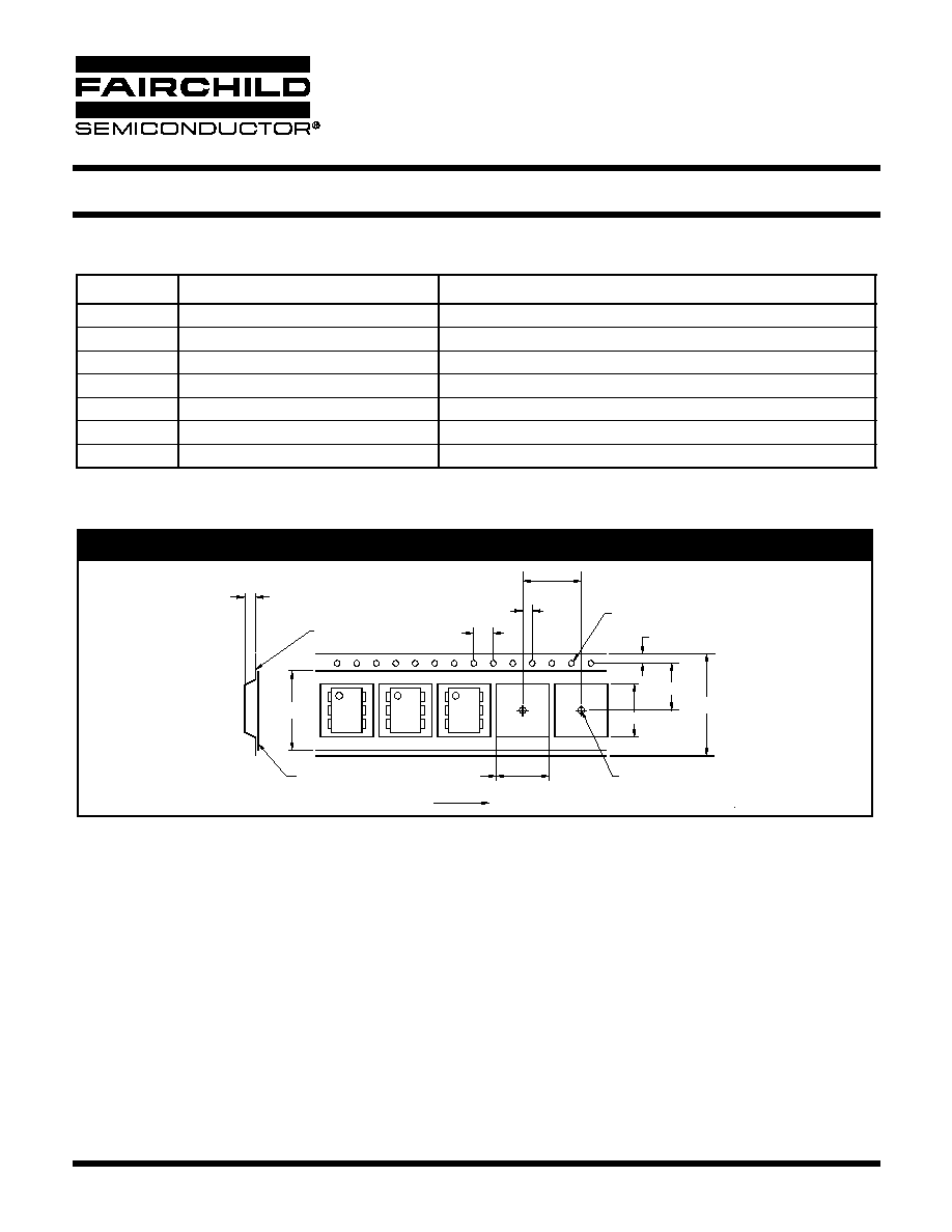
ORDERING INFORMATION
NOTE
All dimensions are in inches (millimeters)
Tape and reel quantity is 1,000 units per reel
Option
Order Entry Identifier
Description
S
.S
Surface Mount Lead Bend
SD
.SD
Surface Mount; Tape and Reel
W
.W
0.4" Lead Spacing
300
.300
VDE 0884
300W
.300W
VDE 0884, 0.4" Lead Spacing
3S
.3S
VDE 0884, Surface Mount
3SD
.3SD
VDE 0884, Surface Mount, Tape and Reel
Carrier Tape Specifications
4.0
± 0.1
ÿ1.55
± 0.05
User Direction of Feed
4.0
± 0.1
1.75
± 0.10
7.5
± 0.1
16.0
± 0.3
12.0
± 0.1
0.30
± 0.05
13.2
± 0.2
4.85
± 0.20
0.1 MAX
10.30
± 0.20
9.55
± 0.20
ÿ1.6
± 0.1

LIFE SUPPORT POLICY
FAIRCHILD'S PRODUCTS ARE NOT AUTHORIZED FOR USE AS CRITICAL COMPONENTS IN LIFE SUPPORT DEVICES
OR SYSTEMS WITHOUT THE EXPRESS WRITTEN APPROVAL OF THE PRESIDENT OF FAIRCHILD SEMICONDUCTOR
CORPORATION. As used herein:
1. Life support devices or systems are devices or systems
which, (a) are intended for surgical implant into the body, or
(b) support or sustain life, and (c) whose failure to perform
when properly used in accordance with instructions for use
provided in the labeling, can be reasonably expected to
result in a significant injury of the user.
2. A critical component in any component of a life support
device or system whose failure to perform can be
reasonably expected to cause the failure of the life support
device or system, or to affect its safety or effectiveness.
DISCLAIMER
FAIRCHILD SEMICONDUCTOR RESERVES THE RIGHT TO MAKE CHANGES WITHOUT FURTHER NOTICE TO
ANY PRODUCTS HEREIN TO IMPROVE RELIABILITY, FUNCTION OR DESIGN. FAIRCHILD DOES NOT ASSUME
ANY LIABILITY ARISING OUT OF THE APPLICATION OR USE OF ANY PRODUCT OR CIRCUIT DESCRIBED HEREIN;
NEITHER DOES IT CONVEY ANY LICENSE UNDER ITS PATENT RIGHTS, NOR THE RIGHTS OF OTHERS.
6/24/02
Page 9 of 9
© 2002 Fairchild Semiconductor Corporation
PHOTO FET OPTOCOUPLERS
H11F1 H11F2 H11F3