 | –≠–ª–µ–∫—Ç—Ä–æ–Ω–Ω—ã–π –∫–æ–º–ø–æ–Ω–µ–Ω—Ç: LM239MX | –°–∫–∞—á–∞—Ç—å:  PDF PDF  ZIP ZIP |
©2002 Fairchild Semiconductor Corporation
www.fairchildsemi.com
Rev. 1.0.2
Features
∑ Single or Dual Supply Operation
∑ Wide Range of Supply Voltage
LM2901,LM339/LM339A,LM239/LM239A: 2 ~ 36V
(or
±
1 ~
±
18V)
LM3302: 2 ~ 28V (or ±1 ~ ±14V)
∑ Low Supply Current Drain 800
µ
A Typ.
∑ Open Collector Outputs for Wired and Connectors
∑ Low Input Bias Current 25nA Typ.
∑ Low Input Offset Current
±
2.3nA Typ.
∑ Low Input Offset Voltage
±
1.4mV Typ.
∑ Input Common Mode Voltage Range Includes Ground.
∑ Low Output Saturation Voltage
∑ Output Compatible With TTL, DTL and MOS Logic
System
Description
The LM2901, LM339/LM339A ,LM239/LM239A, LM3302
consist of four independent voltage comparators designed
to operate from single power supply over a wide voltage
range.
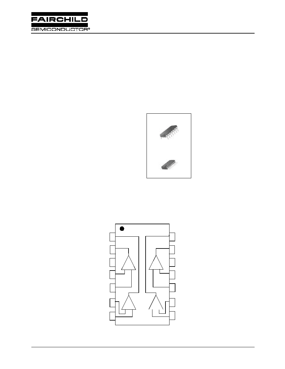
14-SOP
14-DIP
1
1
Internal Block Diagram
14
1
13
12
11
10
9
8
2
3
4
5
6
7
-
+
-
-
+
+
+
-
OUT3
OUT4
IN4(+)
GND
IN4(-)
IN3(+)
IN3(-)
OUT2
OUT1
IN1(+)
IN1(-)
IN2(-)
IN2(+)
V
CC
LM2901,LM339/LM339A,LM3302
LM239/LM239A
Quad Comparator
LM2901,LM339/LM339A,LM3302 LM239/LM239A
2
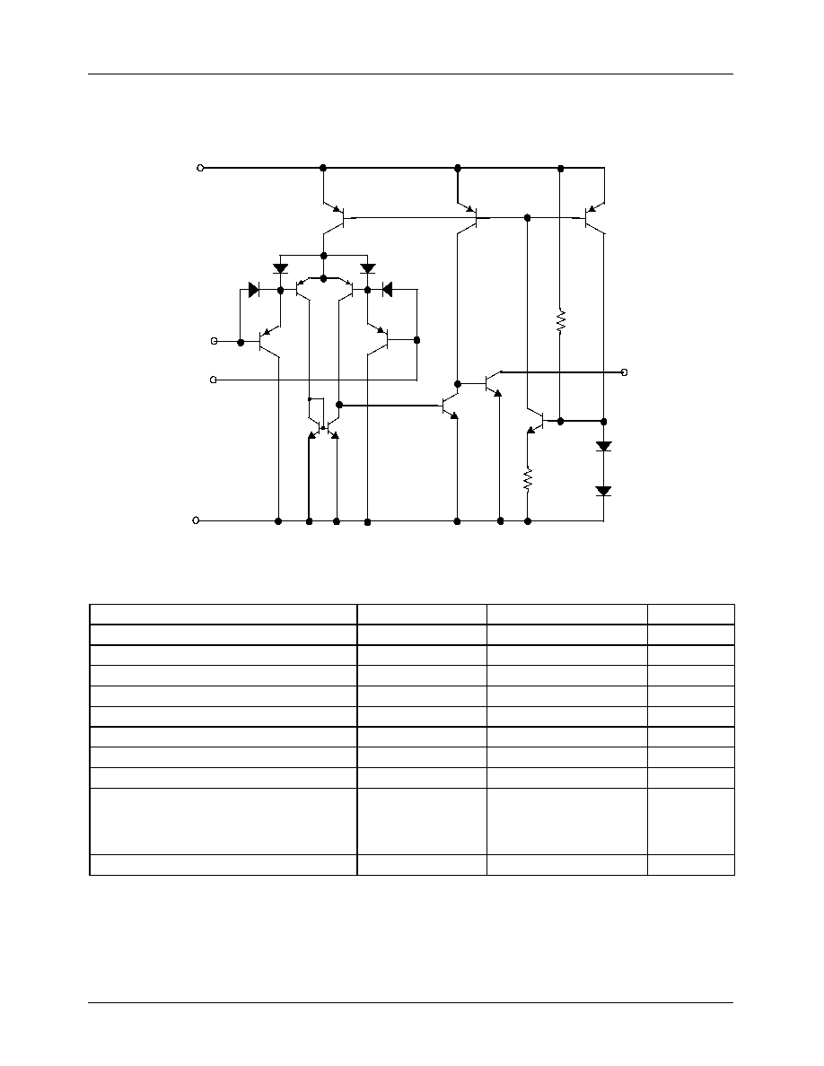
Schematic Diagram
Absolute Maximum Ratings
Parameter
Symbol
Value
Unit
Supply Voltage
V
CC
±
18 or 36
V
Supply Voltage only LM3302
V
CC
±
14 or 28
V
Differential Input Voltage
V
I(DIFF)
36
V
Differential Input Voltage Only LM3302
V
I(DIFF)
28
V
Input Voltage
V
I
-0.3 to +36
V
Input Voltage Only LM3302
V
I
-0.3 to +28
V
Output Short Circuit to GND
-
Continuous
-
Power Dissipation
P
D
570
mW
Operating Temperature
LM339/LM339A
LM2901/LM3302
LM239/LM239A
T
OPR
0 ~ +70
-40 ~ +85
-25 ~ +85
∞
C
Storage Temperature
T
STG
-65 ~ +150
∞
C
V
CC
Q9
Q12
Q14
Q3
Q1
Q2
Q7
Q13
Q8
Q5
Q6
Q4
D4
D5
D6
D1
D2
D3
R2
R1
GND
OUTPUT
IN(-)
IN(+)

LM2901,LM339/LM339A,LM3302 LM239/LM239A
3
Electrical Characteristics
(V
CC
= 5V, T
A
= 25
∞
C, unless otherwise specified)
Note:
1. LM339/LM339A : 0
T
A
+70
∞
C
LM2901/LM3302 : -40
T
A
+85
∞
C
LM239/LM239A : -25
T
A
+85
∞
C
2. These parameters, although guaranteed, are not 100% tested in production.
Parameter
Symbol
Conditions
LM239A/LM339A
LM239/LM339
Unit
Min.
Typ.
Max.
Min. Typ.
Max.
Input Offset
Voltage
V
IO
V
O(P)
=1.4V, R
S
= 0
-
1
2
-
1.4
5
mV
Note1
-
-
4.0
-
-
9.0
Input Offset
Current
I
IO
I
IN(+)
- I
IN(-)
, V
CM
= 0V
-
2.3
50
-
2.3
50
nA
Note1
-
-
150
-
-
150
Input Bias Current
I
BIAS
V
CM
= 0V
-
57
250
-
57
250
nA
Note1
-
-
400
-
-
400
Input Common
Mode Voltage
Range
V
I(R)
V
CC
= 30V
0
-
V
CC
-1.5
0
-
V
CC
-1.5
V
Note1
0
-
V
CC
-2
0
-
V
CC
-2
Supply Current
I
CC
V
CC
= 5V, R
L
=
-
1.1
2.0
-
1.1
2.0
mA
Voltage Gain
G
V
V
CC
=15V, R
L
15k
(for large swing)
50
200
-
50
200
-
V/mV
Large Signal
Response Time
T
LRES
V
I
= TTL Logic Swing
V
REF
= 1.4V, V
RL
= 5V,
R
L
= 5.1k
(Note2)
-
300
-
-
300
-
ns
Response Time
T
RES
V
RL
= 5V, R
L
= 5.1k
(Note2)
-
1.3
-
-
1.3
-
µ
s
Output Sink
Current
I
SINK
V
I(-)
1V, V
I(+)
= 0V,
V
O(P)
1.5V
6
18
-
6
18
-
mA
Output Saturation
Voltage
V
SAT
V
I(-)
1V, V
I(+)
= 0V
-
140
400
-
140
400
mV
I
SINK
= 4mA
Note1
-
-
700
-
-
700
Output Leakage
Current
I
o(LKG)
V
I(-)
= 0V
V
I(+)
= 1V
V
O(P)
= 5V
-
0.1
-
-
0.1
-
nA
V
O(P)
= 30V
-
-
1.0
-
-
1.0
µ
A
Differential Voltage V
I(DIFF)
Note1
-
-
36
-
-
36
V

LM2901,LM339/LM339A,LM3302 LM239/LM239A
4
Electrical Characteristics
(Continued)
(V
CC
= 5V, T
A
= 25
∞
C, unless otherwise specified)
Note:
1. LM339/LM339A : 0
T
A
+70
∞
C
LM2901/LM3302 : -40
T
A
+85
∞
C
LM239/LM239A : -25
T
A
+85
∞
C
2. These parameters, although guaranteed, are not 100% tested in production.
Parameter
Symbol
Conditions
LM2901
LM3302
Unit
Min. Typ. Max. Min. Typ. Max.
Input Offset Voltage
V
IO
V
O(P)
=1.4V, R
S
= 0
-
2
7
-
2
20
mV
Note1
-
9
15
-
-
40
Input Offset Current
I
IO
-
2.3
50
-
3
100
nA
Note1
-
50
200
-
-
300
Input Bias Current
I
BIAS
-
57
250
-
57
250
nA
Note1
-
200
500
-
-
1000
Input Common
Mode Voltage
Range
V
I(R)
LM2901, V
CC
=30V
LM3302, V
CC
=28V
0
-
V
CC
-1.5
0
-
V
CC
-1.5
V
Note1
0
-
V
CC
-2
0
-
V
CC
-2
Supply Current
I
CC
R
L
=
, V
CC
=5V
-
1.1
2.0
-
1.1
2.0
mA
R
L
=
,V
CC
=30V
(LM3302, V
CC
=28V)
-
1.6
2.5
-
1.6
2.5
Voltage Gain
G
V
V
CC
=15V, R
L
15k
(for large swing)
25
100
-
2
30
-
V/
mV
Large Signal
Response Time
T
LRES
V
I
=TTL Logic Swing
V
REF
=1.4V, V
RL
=5V, R
L
=5.1k
(Note2)
-
300
-
-
300
-
ns
Response Time
T
RES
V
RL
= 5V, R
L
= 5.1k
(Note2)
-
1.3
-
-
1.3
-
µ
s
Output Sink Current
I
SINK
V
I(-)
1V, V
I(+)
=0V, V
O(P)
1.5V
6
18
-
6
18
-
mA
Output Saturation
Voltage
V
SAT
V
I(-)
1V, V
I(+)
= 0V
-
140
400
-
140
400
mV
I
SINK
=4mA
Note1
-
-
700
-
-
700
Output Leakage
Current
I
O(LKG)
V
I(-)
= 0V
V
I(+)
= 1V
V
O(P)
= 5V
-
0.1
-
-
0.1
-
nA
V
O(P)
= 30V
-
-
1.0
-
-
1.0
µ
A
Differential Voltage V
I(DIFF)
Note1
-
-
36
-
-
28
V

LM2901,LM339/LM339A,LM3302 LM239/LM239A
5
Typical Performance Characteristics
Figure 1. Supply Current vs Supply Voltage
Figure 2. Input Current vs Supply Voltage
Figure 3. Output Saturation Voltage vs Sink Current
Figure 4. Response Time for Various Input
Overdrive-Negative Transition
Figure 5. Response Time for Various Input
Overdrive-Positive Transition