 | –≠–ª–µ–∫—Ç—Ä–æ–Ω–Ω—ã–π –∫–æ–º–ø–æ–Ω–µ–Ω—Ç: LM741IN | –°–∫–∞—á–∞—Ç—å:  PDF PDF  ZIP ZIP |

©2001 Fairchild Semiconductor Corporation
www.fairchildsemi.com
Rev. 1.0.1
Features
∑ Short circuit protection
∑ Excellent temperature stability
∑ Internal frequency compensation
∑ High Input voltage range
∑ Null of offset
Description
The LM741 series are general purpose operational amplifi-
ers. It is intended for a wide range of analog applications.
The high gain and wide range of operating voltage provide
superior performance in intergrator, summing amplifier, and
general feedback applications.
8-DIP
1
8-SOP
1
Internal Block Diagram
LM741
Single Operational Amplifier

LM741
2
Schematic Diagram
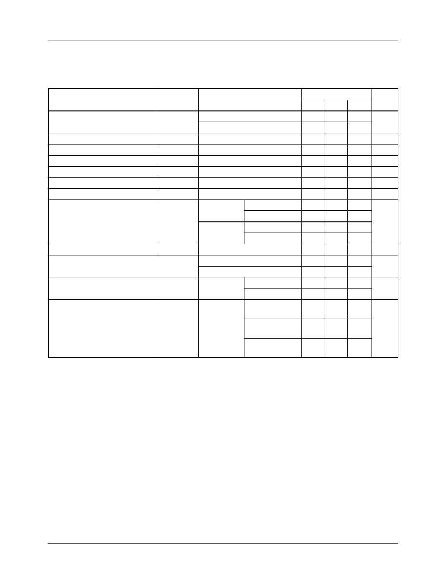
Absolute Maximum Ratings (T
A
= 25
∞
C)
Parameter
Symbol
Value
Unit
Supply Voltage
V
CC
±
18
V
Differential Input Voltage
V
I(DIFF)
30
V
Input Voltage
V
I
±
15
V
Output Short Circuit Duration
-
Indefinite
-
Power Dissipation
P
D
500
mW
Operating Temperature Range
LM741C
LM741I
T
OPR
0 ~ + 70
-40 ~ +85
∞
C
Storage Temperature Range
T
STG
-65 ~ + 150
∞
C

LM741
3
Electrical Characteristics
(V
CC
= 15V, V
EE
= - 15V. T
A
= 25
∞
C, unless otherwise specified)
Note:
1. Guaranteed by design.
Parameter
Symbol
Conditions
LM741C/LM741I
Unit
Min.
Typ.
Max.
Input Offset Voltage
V
IO
R
S
10K
-
2.0
6.0
mV
R
S
50
-
-
-
Input Offset Voltage
Adjustment Range
V
IO(R)
V
CC
=
±
20V
-
±
15
-
mV
Input Offset Current
I
IO
-
-
20
200
nA
Input Bias Current
I
BIAS
-
-
80
500
nA
Input Resistance (Note1)
R
I
V
CC
=
±
20V
0.3
2.0
-
M
Input Voltage Range
V
I(R)
-
±
12
±
13
-
V
Large Signal Voltage Gain
G
V
R
L
2K
V
CC
=
±
20V,
V
O(P-P)
=
±
15V
-
-
-
V/mV
V
CC
=
±
15V,
V
O(P-P)
=
±
10V
20
200
-
Output Short Circuit Current
I
SC
-
-
25
-
mA
Output Voltage Swing
V
O(P-P)
V
CC
=
±
20V
R
L
10K
-
-
-
V
R
L
2K
-
-
-
V
CC
=
±
15V
R
L
10K
±
12
±
14
-
R
L
2K
±
10
±
13
-
Common Mode Rejection Ratio
CMRR
R
S
10K
, V
CM
=
±
12V
70
90
-
dB
R
S
50
, V
CM
=
±
12V
-
-
-
Power Supply Rejection Ratio
PSRR
V
CC
=
±
15V to V
CC
=
±
15V
R
S
50
-
-
-
dB
V
CC
=
±
15V to V
CC
=
±
15V
R
S
10K
77
96
-
Transient
Rise Time
T
R
Unity Gain
-
0.3
-
µ
s
Response
Overshoot
OS
-
10
-
%
Bandwidth
BW
-
-
-
-
MHz
Slew Rate
SR
Unity Gain
-
0.5
-
V/
µ
s
Supply Current
I
CC
R
L
=
-
1.5
2.8
mA
Power Consumption
P
C
V
CC
=
±
20V
-
-
-
mW
V
CC
=
±
15V
-
50
85
LM741
4
Electrical Characteristics
( 0
∞
C
T
A
70
∞
C V
CC
=
±
15V, unless otherwise specified)
The following specification apply over the range of 0
∞
C
T
A
+70
∞
C for the LM741C; and the -40
∞
C
T
A
+85
∞
C
for the LM741I
Note :
1. Guaranteed by design.
Parameter
Symbol
Conditions
LM741C/LM741I
Unit
Min.
Typ.
Max.
Input Offset Voltage
V
IO
R
S
50
-
-
-
mV
R
S
10K
-
-
7.5
Input Offset Voltage Drift
V
IO
/
T
-
-
-
µ
V/
∞
C
Input Offset Current
I
IO
-
-
-
300
nA
Input Offset Current Drift
I
IO
/
T
-
-
-
nA/
∞
C
Input Bias Current
I
BIAS
-
-
-
0.8
µ
A
Input Resistance (Note1)
R
I
V
CC
=
±
20V
-
-
-
M
Input Voltage Range
V
I(R)
-
±
12
±
13
-
V
Output Voltage Swing
V
O(P-P)
V
CC
=
±
20V
R
S
10K
-
-
-
V
R
S
2K
-
-
-
V
CC
=
±
15V
R
S
10K
±
12
±
14
-
R
S
2K
±
10
±
13
-
Output Short Circuit Current
I
SC
-
10
-
40
mA
Common Mode Rejection Ratio
CMRR
R
S
10K
, V
CM
=
±
12V
70
90
-
dB
R
S
50
, V
CM
=
±
12V
-
-
-
Power Supply Rejection Ratio
PSRR
V
CC
=
±
20V
to
±
5V
R
S
50
-
-
-
dB
R
S
10K
77
96
-
Large Signal Voltage Gain
G
V
R
S
2K
V
CC
=
±
20V,
V
O(P-P)
=
±
15V
-
-
-
V/mV
V
CC
=
±
15V,
V
O(P.P)
=
±
10V
15
-
-
V
CC
=
±
15V,
V
O(P-P)
=
±
2V
-
-
-

LM741
5
Typical Performance Characteristics
Figure 1. Output Resistance vs Frequency
Figure 2. Input Resistance and Input
Capacitance vs Frequency
Figure 3. Input Bias Current vs Ambient Temperature
Figure 4. Power Consumption vs Ambient Temperature
Figure 5. Input Offset Current vs Ambient Temperature
Figure 6. Input Resistance vs Ambient Temperature