
May 1998
NDT3055
N-Channel Enhancement Mode Field Effect Transistor
General Description Features
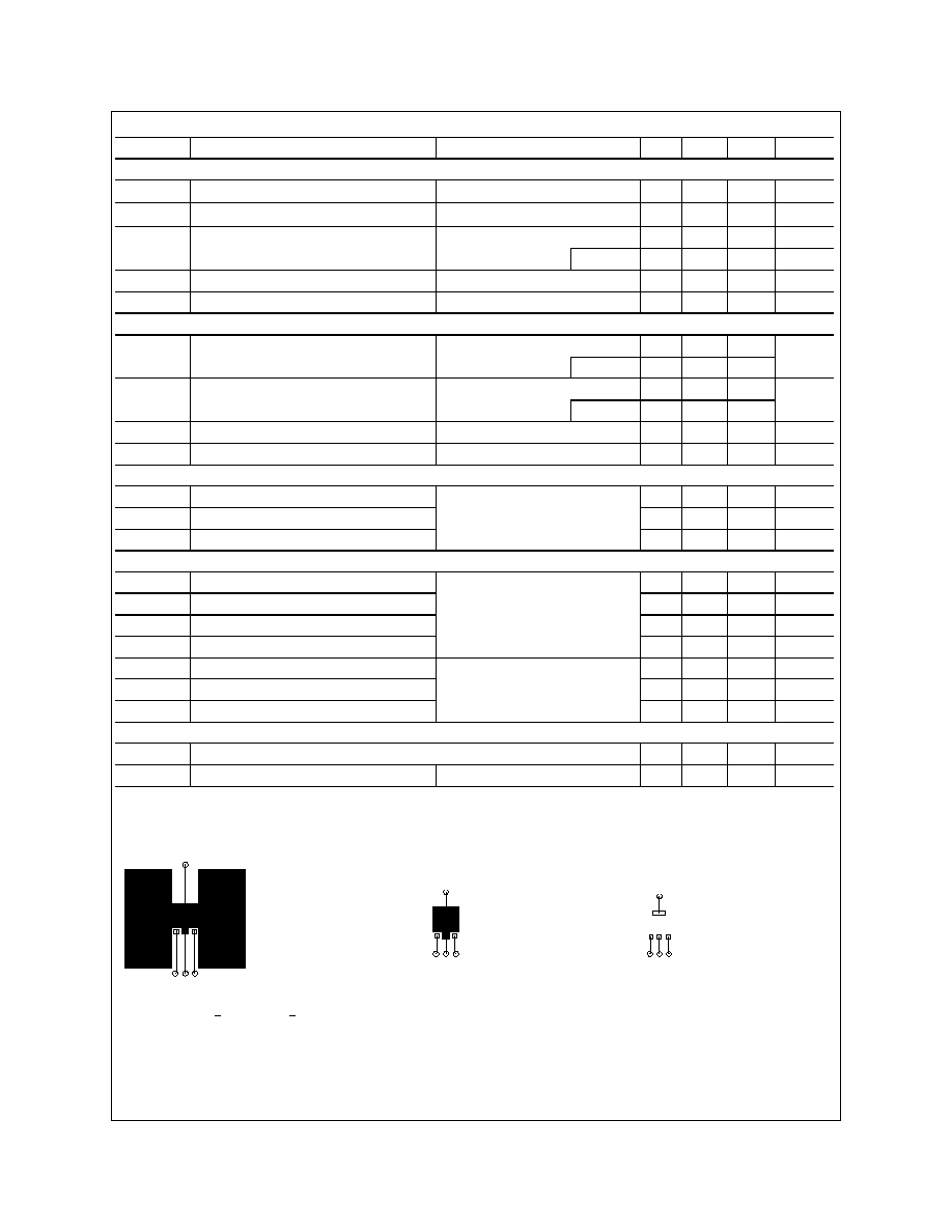
Absolute Maximum Ratings
T
A
= 25
o
C unless otherwise noted
Symbol
Parameter
NDT3055
Units
V
DSS
Drain-Source Voltage
60
V
V
GSS
Gate-Source Voltage - Continuous
�20
V
I
D
Maximum Drain Current - Continuous
(Note 1a)
4
A
- Pulsed
25
P
D
Maximum Power Dissipation
(Note 1a)
3
W
(Note 1b)
1.3
(Note 1c)
1.1
T
J
,T
STG
Operating and Storage Temperature Range
-65 to 150
�C
THERMAL CHARACTERISTICS
R
JA
Thermal Resistance, Junction-to-Ambient
(Note 1a)
42
�C/W
R
JC
Thermal Resistance, Junction-to-Case
(Note 1)
12
�C/W
* Order option J23Z for cropped center drain lead.
NDT3055 Rev.B
4 A, 60 V. R
DS(ON)
= 0.100
@ V
GS
= 10 V.
High density cell design for extremely low R
DS(ON)
.
High power and current handling capability in a widely used
surface mount package.
SOIC-16
SuperSOT
TM
-3
SuperSOT
TM
-8
SO-8
SOT-223
SuperSOT
TM
-6
These N-Channel enhancement mode power field effect
transistors are produced using Fairchild's proprietary,
high cell density, DMOS technology. This very high
density process is especially tailored to minimize
on-state resistance and provide superior switching
performance.
These devices are particularly suited for
low voltage applications such as DC motor control and
DC/DC conversion where fast switching, low in-line
power loss, and resistance to transients are needed.
G
D
S
D
SOT-223
D
D
S
G
G
D
S
SOT-223*
(J23Z)
D
S
G
� 1998 Fairchild Semiconductor Corporation
Electrical Characteristics
(T
A
= 25
O
C unless otherwise noted )
Symbol
Parameter
Conditions
Min
Typ
Max
Units
OFF CHARACTERISTICS
BV
DSS
Drain-Source Breakdown Voltage
V
GS
= 0 V, I
D
= 250 �A
60
V
BV
DSS
/
T
J
Breakdown Voltage Temp. Coefficient
I
D
= 250 �A, Referenced to 25
o
C
63
mV/
o
C
I
DSS
Zero Gate Voltage Drain Current
V
DS
= 48 V, V
GS
= 0 V
10
�A
T
J
=125�C
100
�A
I
GSSF
Gate - Body Leakage, Forward
V
GS
= 20 V, V
DS
= 0 V
100
nA
I
GSSR
Gate - Body Leakage, Reverse
V
GS
= -20 V, V
DS
= 0 V
-100
nA
ON CHARACTERISTICS
(Note 2)
V
GS(th)
Gate Threshold Voltage
V
DS
= V
GS
, I
D
= 250 �A
2
3
4
V
T
J
=125�C
1.5
2.4
3
R
DS(ON)
Static Drain-Source On-Resistance
V
GS
= 10 V, I
D
= 4 A
0.084
0.1
T
J
=125�C
0.14
0.18
I
D(ON)
On-State Drain Current
V
GS
= 10 V, V
DS
= 10 V
15
A
g
FS
Forward Transconductance
V
DS
= 15 V, I
D
= 4 A
6
S
DYNAMIC CHARACTERISTICS
C
iss
Input Capacitance
V
DS
= 30 V, V
GS
= 0 V,
f = 1.0 MHz
250
pF
C
oss
Output Capacitance
100
pF
C
rss
Reverse Transfer Capacitance
30
pF
SWITCHING CHARACTERISTICS
(Note 2)
t
D(on)
Turn - On Delay Time
V
DD
= 25 V, I
D
= 1.2 A,
V
GS
= 10 V, R
GEN
= 50
10
25
ns
t
r
Turn - On Rise Time
18
50
ns
t
D(off)
Turn - Off Delay Time
37
65
ns
t
f
Turn - Off Fall Time
30
60
ns
Q
g
Total Gate Charge
V
DS
= 40 V, I
D
= 4 A,
V
GS
= 10 V
9
15
nC
Q
gs
Gate-Source Charge
2.3
nC
Q
gd
Gate-Drain Charge
2.6
nC
DRAIN-SOURCE DIODE CHARACTERISTICS AND MAXIMUM RATINGS
I
S
Maximum Continuous Drain-Source Diode Forward Current
2.5
A
V
SD
Drain-Source Diode Forward Voltage
V
GS
= 0 V, I
S
= 2.5 A
(Note 2)
0.85
1.2
V
Notes:
1. R
JA
is the sum of the junction-to-case and case-to-ambient thermal resistance where the case thermal reference is defined as the solder mounting surface of the drain pins. R
JC
is
guaranteed by design while R
CA
is determined by the user's board design.
Typical R
JA
using the board layouts shown below on FR-4 PCB in a still air environment:
Scale 1 : 1 on letter size paper
2. Pulse Test: Pulse Width < 300�s, Duty Cycle < 2.0%
NDT3055 Rev.B
a. 42
o
C/W when mounted on a 1 in
2
pad of
2oz Cu.
b. 95
o
C/W when mounted on a 0.066 in
2
pad of 2oz Cu.
c. 110
o
C/W when mounted on a 0.00123
in
2
pad of 2oz Cu.

NDT3055 Rev.B
Typical Electrical Characteristics
Figure 1. On-Region Characteristics.
Figure 2. On-Resistance Variation with
Drain Current and Gate Voltage.
Figure 3. On-Resistance Variation
with Temperature.
Figure 5. Transfer Characteristics.
Figure 4. On-Resistance Variation with
Gate-to- Source Voltage.
-50
-25
0
25
50
75
100
125
150
0.4
0.8
1.2
1.6
2
T , JUNCTION TEMPERATURE (�C)
DRAIN-SOURCE ON-RESISTANCE
J
V =10V
GS
I = 4A
D
R , NORMALIZED
DS(ON)
0
1
2
3
4
5
0
3
6
9
12
15
V , DRAIN-SOURCE VOLTAGE (V)
I , DRAIN-SOURCE CURRENT (A)
DS
D
V =10V
GS
6.0V
4.5V
5.0V
7.0V
5.5V
8.0V
0
4
8
12
16
20
0.5
1
1.5
2
2.5
3
I , DRAIN CURRENT (A)
DRAIN-SOURCE ON-RESISTANCE
V = 5.5V
GS
D
R , NORMALIZED
DS(ON)
6.0V
10V
8.0V
7.0V
6.5V
2
4
6
8
0
2
4
6
8
10
V , GATE TO SOURCE VOLTAGE (V)
I , DRAIN CURRENT (A)
25�C
125�C
V = 10V
DS
GS
D
T = -55�C
J
0
0.2
0.4
0.6
0.8
1
1.2
0.0001
0.001
0.01
0.1
1
10
V , BODY DIODE FORWARD VOLTAGE (V)
I , REVERSE DRAIN CURRENT (A)
T = 125�C
A
25�C
-55�C
V = 0V
GS
SD
S
Figure 6. Body Diode Forward Voltage
Variation with Current and
Temperature.
4
6
8
10
0
0.1
0.2
0.3
0.4
V , GATE TO SOURCE VOLTAGE (V)
R
, ON-RESISTANCE (OHM)
DS(ON)
GS
T = 25�C
A
T = 125�C
A
I = 2A
D

NDT3055 Rev.B
Figure 10. Single Pulse Maximum Power
Dissipation.
Figure 8. Capacitance Characteristics.
Figure 7. Gate Charge Characteristics.
Figure 9. Maximum Safe Operating Area.
Typical Electrical Characteristics
(continued)
0.0001
0.001
0.01
0.1
1
10
100
300
0.001
0.002
0.005
0.01
0.02
0.05
0.1
0.2
0.5
1
t , TIME (sec)
TRANSIENT THERMAL RESISTANCE
r(t), NORMALIZED EFFECTIVE
1
Single Pulse
D = 0.5
0.1
0.05
0.02
0.01
0.2
Duty Cycle, D = t / t
1
2
R (t) = r(t) * R
R = 110 �C/W
T - T = P * R (t)
A
J
P(pk)
t
1
t
2
JA
JA
JA
JA
Figure 11. Transient Thermal Response Curve.
Thermal characterization performed using the conditions described in note 1c.
Transient thermal response will change depending on the circuit board design.
0.1
0.3
1
4
10
30
60
10
20
50
100
200
500
1000
V , DRAIN TO SOURCE VOLTAGE (V)
CAPACITANCE (pF)
DS
C
iss
f = 1 MHz
V = 0V
GS
C
oss
C
rss
0
3
6
9
12
15
0
3
6
9
12
15
Q , GATE CHARGE (nC)
V , GATE-SOURCE VOLTAGE (V)
g
GS
I = 4A
D
V = 10V
DS
40V
20V
0.1
0.2
0.5
1
2
5
10
30
60 100
0.01
0.03
0.1
0.3
1
3
10
50
V , DRAIN-SOURCE VOLTAGE (V)
I , DRAIN CURRENT (A)
DS
D
1s
100ms
10s
10ms
RDS(ON) LIMIT
1ms
DC
V = 10V
SINGLE PULSE
R = 110 C/W
T = 25�C
GS
A
JA
o
100us
0.001
0.01
0.1
1
10
100
300
0
20
40
60
80
SINGLE PULSE TIME (SEC)
POWER (W)
SINGLE PULSE
R =110�C/W
T = 25�C
JA
A

SOT-223 Packaging
Configuration: Figure 1.0
Components
Leader Tape
500mm minimum or
62 empty pockets
Trailer Tape
300mm minimum or
38 empty pockets
SOT-223 Tape Leader and Trailer
Configuration: Figure 2.0
Cover Tape
Carrier Tape
Note/Comments
Packaging Option
SOT-223 Packaging Information
Standard
(no flow code)
D84Z
Packaging type
Reel Size
TNR
13" Dia
TNR
7" Dia
Qty per Reel/Tube/Bag
2,500
500
Box Dimension (mm)
343x64x343
184x187x47
Max qty per Box
5,000
1,000
Weight per unit (gm)
0.1246
0.1246
Weight per Reel (kg)
0.7250
0.1532
SOT-223 Unit Orientation
F852
014
F852
014
F852
014
F852
014
F63TNR Label
343mm x 342mm x 64mm
Intermediate box for Standard
184mm x 184mm x 47mm
Pizza Box for D84Z Option
F63TNR Label
LOT: CBVK741B019
FSID: PN2222A
D/C1: D9842 QTY1:
SPEC REV:
SPEC:
QTY: 3000
D/C2:
QTY2:
CPN:
N/F: F (F63TNR)3
F63TNR Label sample
F63TNR Label
Antistatic Cover Tape
Customized Label
Static Dissipative
Embossed Carrier Tape
Packaging Description:
SOT-223 parts are shipped in tape. The carrier tape is
made from a dissipative (carbon filled) polycarbonate
resin. The cover tape is a multilayer film (Heat Activated
Adhesive in nature) primarily composed of polyester film,
adhesive layer, sealant, and anti-static sprayed agent.
These reeled parts in standard option are shipped with
2,500 units per 13" or 330cm diameter reel. The reels are
dark blue in color and is made of polystyrene plastic (anti-
static coated). Other option comes in 500 units per 7" or
177cm diameter reel. This and some other options are
further described in the Packaging Information table.
These full reels are individually barcode labeled and
placed inside a standard intermediate box (illustrated in
figure 1.0) made of recyclable corrugated brown paper.
One box contains two reels maximum. And these boxes
are placed inside a barcode labeled shipping box which
comes in different sizes depending on the number of parts
shipped.
SOT-223 Tape and Reel Data and Package Dimensions
September 1999, Rev. B