 | –≠–ª–µ–∫—Ç—Ä–æ–Ω–Ω—ã–π –∫–æ–º–ø–æ–Ω–µ–Ω—Ç: R1152N | –°–∫–∞—á–∞—Ç—å:  PDF PDF  ZIP ZIP |
'2004.4.8
PRELIMINARY
High Input Voltage Tolerant Boost Voltage Regulator
R1152N SERIES
Rev. 1.10
- 1 -
s
OUTLINE
The R1152N series are CMOS-based boost type voltage regulator ICs with high output voltage accuracy and low supply
current. The output voltage of these ICs is internally fixed with high accuracy,
±
2%. Since the package for these ICs is
SOT-23-5 (Mini-mold) package.
s
FEATURES
z Ultra-Low Supply Current......................................... Typ. 10
µ
A
z Standby Mode............................................................ Typ. 0.1
µ
A
z High Output Voltage Accuracy.................................. ±2.0%
z Small Package .........................................................SOT-23-5(Mini-mold)
z Output Voltage...........................................................Stepwise setting with a step of 0.1V in the range of 2.5V to
12.0V(Fixed type) or adjustable (with external divider resistors, the
reference voltage is 2.5V)
z Built-in Current Limit Circuit
z Output Short Current Limit Circuit
z Operating Input Voltage.............................................Max. 18V
s
APPLICATIONS
z Power source for home appliances such as refrigerators, rice cookers, etc.
z Power source for car audio equipment, car navigation system, and ETC system.
z Power source for notebook PCs, digital TVs, cordless phones, and LAN system.
z Power source for copiers, printers, facsimiles, and scanners.
s
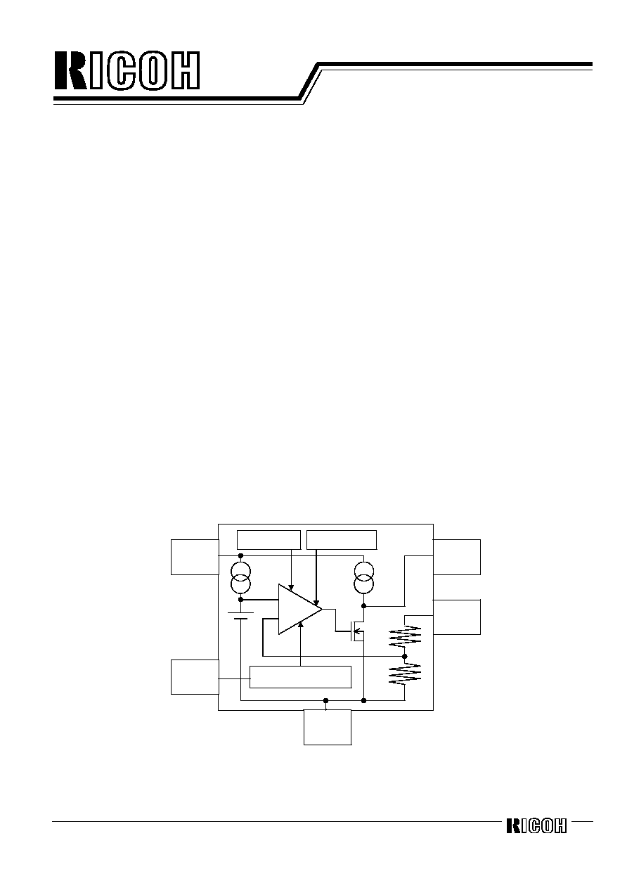
BLOCK DIAGRAMS
V
IN
CE
EXT
V
OUT
GND
Chip Enable Circuit
+
-
Short Current
Limit
Peak Current Limit
Rev. 1.10
- 2 -
s
SELECTION GUIDE
The output voltage, mask option code, and the taping type for the ICs can be selected at the user's request. The selection
can be made with designating the part number as shown below;
R1152NXXXB-XX
Part Number
a b c
Code Contents
a
Designation of Voltage Setting:
0.1V Stepwise Setting in the range from 2.5V to 12.0V (Fixed)
b
Chip Enable Polarity:
B: with CE (active at "H" type)
c
Designation of Taping Type :
Ex. TR (Refer to Taping Specifications.)
s
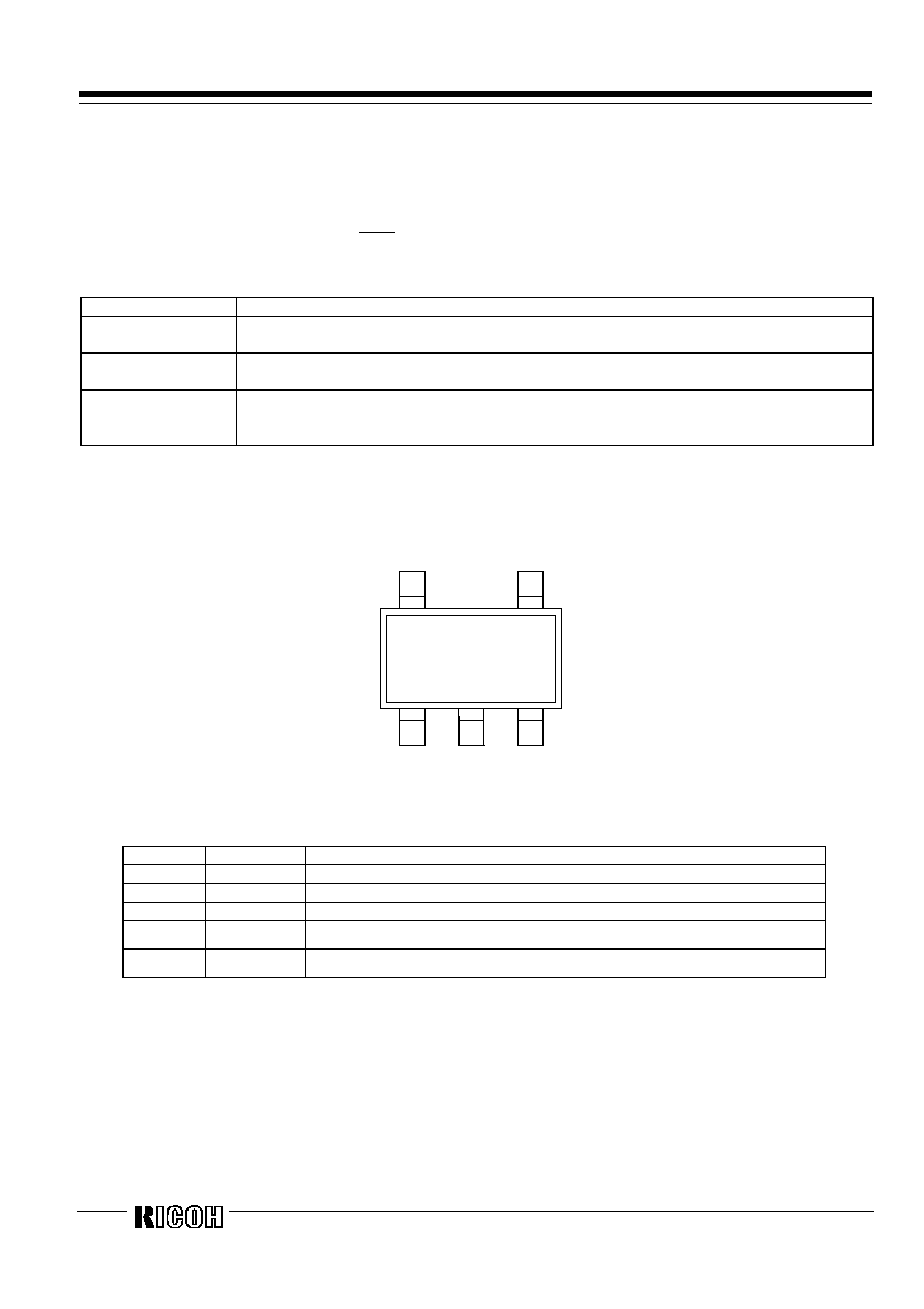
PIN CONFIGURATION
SOT-23-5
5
4
1
2
3
(mark side)
s
PIN DESCRIPTIONS
Pin No.
Symbol
Description
1
CE
Chip Enable Pin
2
GND Ground
Pin
3
V
IN
Input
Pin
4
EXT
External Transistor Drive Pin
5 V
OUT
Voltage Regulator Output Pin

Rev. 1.10
-3 -
s
ABSOLUTE MAXIMUM RATINGS
Item Symbol
Rating
Unit
Input Voltage
V
IN
20 V
Peak Input Voltage
*Note1
V
PEAK
26 V
Input Voltage(CE Pin)
V
CE
-0.3 ~ V
IN
+0.3
20
V
Output Voltage(V
OUT
Pin)
V
OUT
-0.3 ~ V
IN
+0.3
20
V
Output Voltage(EXT Pin)
V
EXT
-0.3 ~ V
IN
+0.3
20
V
EXT Output Current
I
EXT
25 mA
Power Dissipation
P
D
150
mW
Operating Temperature Range
Topt
-40 ~ +105
∞
C
Storage Temperature Range
Tstg
-55 ~ +125
∞
C
*Note 1 Duration=200ms
s
ELECTRICAL CHARACTERISTICS
q
R1152NXX2X
Topt=25
∞
C
Symbol Item
Conditions Min.
Typ.
Max.
Unit
V
OUT
Output
Voltage
V
IN
= Set V
OUT
+1V
I
OUT
= 100mA
V
OUT
◊
0.98
V
OUT
◊
1.02
V
I
OUT
Output
Current
V
IN
- V
OUT
= 1.0V
1
Note
A
V
OUT
/
I
OUT
Load
Regulation
V
IN
= Set V
OUT
+1V
1mA
I
OUT
100mA
Refer to the specification table by
output voltage
V
DIF
Dropout
Voltage
I
OUT
= 300mA
Refer to the specification table by
output voltage
I
SS
Supply
Current
V
IN
= Set V
OUT
+1V, I
OUT
= 0mA
10
24
µ
A
Istandby Supply
Current
(Standby) V
IN
= 18V V
CE
=0V
0.1
1.0
µ
A
V
OUT
/
V
IN
Line
Regulation
Set V
OUT
+0.5V
V
IN
18V
I
OUT
= 100mA
0.01
0.10
%/V
V
IN
Input
Voltage
18 V
V
OUT
/
T
Output Voltage
Temperature Coefficient
I
OUT
= 100mA
-40
∞
C
Topt
105
∞
C
±50 ppm
/
∞
C
Ilim Current
Limit
Refer to the specification Table
Base Current I
B
of PNP Tr.
10 25
mA
I
RPT
Short
Current
Limit
Base Current I
B
of PNP Tr.
V
OUT
= 0V
600
µ
A
V
CEH
CE Input Voltage "H"
2.0
V
IN
V
V
CEL
CE Input Voltage "L"
0.0
0.5
V
Note: This item depends on the capability of external PNP transistor. Use low saturation type transistor with hFE value range
of 100 to 300.
z Load Regulation Table (Topt=25
∞
C)
Output Voltage V
OUT
(V)
Load Regulation (mV)
Typ.
Max.
2.5V
V
OUT
5.0V
4 10
5.0V<V
OUT
12.0V
4 18
z Dropout Voltage Table (Topt=25
∞
C)
Output Voltage V
OUT
(V) Dropout
Voltage
(mV)
Typ.
Max.
2.5V
V
OUT
<5.0V
150 290
5.0V
V
OUT
12.0V
100 180
*This specification depends on an external transistor. ("2SB1642" is the reference item.)

Rev. 1.10
- 4 -
z Output Current Limit Condition Table (Topt=25
∞
C)
Output Voltage V
OUT
(V) Condition
2.5V
V
OUT
<4.0V
V
IN
=5.0V
4.0V
V
OUT
12.0V
V
IN
=V
OUT
+1.0V
s
OPERATION
In these ICs, fluctuation of Output Voltage, V
OUT
is detected by the feed-back registers, and the result is compared with a
reference voltage with the error amplifier and control the base current of an external PNP transistor so that a constant
voltage is output. The base current is monitored with the base current limit circuit. If the base current may be too large, the
protection circuit works.
s
TECHNICAL NOTES
When using these ICs, consider the following points:
In these ICs, phase compensation is made for securing stable operation even if the load current is varied. For this purpose,
be sure to use a capacitor as C
L
with good frequency characteristics and appropriate ESR (Equivalent Series Resistance).
Make V
DD
and GND lines sufficient. When their impedance is high, noise pickup or unstable operation may result.
Set external components, especially 10
µ
F or more output capacitor, as close as possible to the ICs.
If you choose an electrolytic capacitor, ESR shift by temperature should be small. If you choose a ceramic capacitor, add
an appropriate series resister.
If hFE value of the PNP transistor is too high, output voltage may rise at low load current (less than 1mA).
When you choose an external transistor, select with considering output current, input voltage, and power dissipation.
Generally, low Vc
E(SAT)
and hFE range from 100 to 300 are the appropriate characteristics.
If the set output voltage is less than 4.0V, and I
OUT
>1A must be obtained, at least V
IN
5.0V is the appropriate condition.
(Supposed as hFE=100)
Voltage level for CE should not be floating, or middle range voltage. If the CE voltage is not appropriate, output voltage
may be unstable or conduction current may flow.
All external components should be located as close as possible to the IC, and wiring should be as short as possible.
s
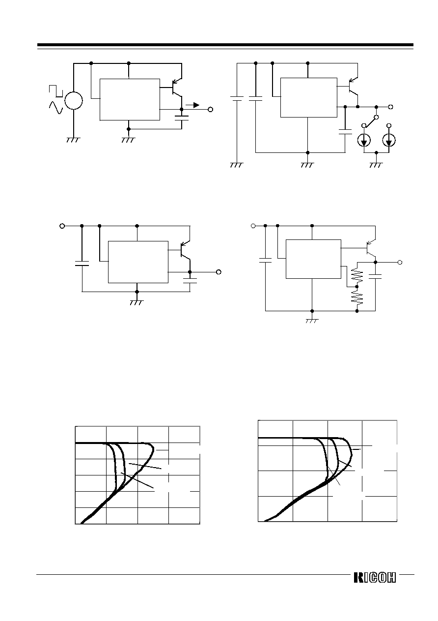
TEST CIRCUITS
VIN
CE
GND
EXT
VOUT
V
IN
OUT
C
IN
C
OUT
PNP Tr
VIN
CE
GND
EXT
VOUT
V
IN
V
OUT
Iss
Fig.1 Standard test Circuit C
IN
=0.1
µ
F, C
OUT
=10
µ
F
Fig.2 Supply Current Test Circuit
Rev. 1.10
-5 -
OUT
VIN
CE
GND
EXT
VOUT
C
OUT
PNP Tr
P.G.
I
OUT
VIN
CE
GND
EXT
VOUT
OUT
C
IN
C
OUT
PNPTr
I1 I2
V
IN
Fig.3 Ripple Rejection, Line Transient Response Test Circuit
C
OUT
=10
µ
F
Fig.4 Load Transient Response Test Circuit
C
IN
=0.1
µ
F, C
OUT
=10
µ
F
s
TYPICAL APPLICATIONS
Fixed Type Output
Adjustable Output
V
IN
CE
GND
EXT
V
OUT
IN
OUT
C
I N
C
OUT
PNP Tr
V
I N
CE
GN D
EXT
V
OUT
IN
OUT
C
I N
C
OU T
PNP Tr
(External Components)
C
IN
=0.1
µ
F, C
OUT
=10
µ
F
s
TYPICAL CHARACTERISTICS
1) Output Voltage vs. Output Current (Topt=25
∞
C)
a. External Tr.: 2SB1642
R1152N025B
0.0
0.5
1.0
1.5
2.0
2.5
3.0
0
500
1000
1500
2000
Output Current I
OUT
(mA)
O
u
t
p
ut
Volt
age V
OUT
(V)
V
IN
=5.0
V
IN
=3.5
V
IN
=3.0V
R1152N033B
0.0
1.0
2.0
3.0
4.0
0
500
1000
1500
2000
Output Current I
OUT
(mA)
O
u
tput V
o
ltage V
OUT
(V
)
V
IN
=5.0V
V
IN
=4.3V
V
IN
=3.8V