 | ÐлекÑÑоннÑй компоненÑ: RMPA2059 | СкаÑаÑÑ:  PDF PDF  ZIP ZIP |
Äîêóìåíòàöèÿ è îïèñàíèÿ www.docs.chipfind.ru

May 2005
RM
P
A
2
0
5
9
WC
DM
A Po
we
r
Ed
g
e
TM
P
o
we
r
A
m
p
lif
ier
M
o
d
u
le
©2005 Fairchild Semiconductor Corporation
1
www.fairchildsemi.com
RMPA2059 Rev. F
RMPA2059
WCDMA PowerEdgeTM Power Amplifier Module
Features
· 40% CDMA efficiency at +27dBm average output power
· Single positive-supply operation and low power and
shutdown modes
· Meets UTMS/WCDMA and HSDPA performance
requirements
· Compact Lead-free compliant LCC package
- 4.0 x 4.0 x 1.5 mm
· Industry standard pinout
· Internally matched to 50
and DC blocked RF input/
output
General Description
The RMPA2059 power amplifier module (PAM) is designed
for WCDMA applications. The 2 stage PAM is internally
matched to 50
to minimize the use of external
components and features a low-power mode to reduce
standby current and DC power consumption during peak
phone usage. High power-added efficiency and excellent
linearity are achieved using our InGaP Heterojunction
Bipolar Transistor (HBT) process.
Functional Block Diagram
Vref
Vmode
RF IN
GND
Vcc1
RF OUT
GND
GND
GND
7
6
8
9
10
4
3
2
BIAS/MODE SWITCH
1
5
Vcc2
11 (paddle ground on package bottom)
INPUT
MATCH
OUTPUT
MATCH
MMIC
(Top View)
Device

RM
P
A
2
0
5
9
WC
DM
A Po
we
r
Ed
g
e
TM
P
o
we
r
A
m
p
lif
ier
M
o
d
u
le
©2005 Fairchild Semiconductor Corporation
2
www.fairchildsemi.com
RMPA2059 Rev. F
Absolute Ratings
1
Note:
1: No permanent damage with only one parameter set at extreme limit. Other parameters set to typical values.
Electrical Characteristics
1
Notes:
1: All parameters met at Tc = +25°C, Vcc = +3.4V, f = 1950MHz, and load VSWR
1.2:1.
2: All phase angles.
3: Guaranteed by design.
Symbol
Parameter
Min
Max
Units
Vcc1, Vcc2
Supply Voltages
0
5.0
V
Vref
Reference Voltage
2.7
5.0
V
Vmode
Power Control Voltage
0
3.0
V
Pin
RF Input Power
+5
dBm
T
STG
Storage Temperature
-55
+150
°C
Symbol
Parameter
Min
Typ
Max
Units
Comments
f
Operating Frequency
1920
1980
MHz
WCDMA Operation
Gp
Power Gain
26.5
dB
Po=+27dBm; Vmode=0V
24
dB
Po=+16dBm; Vmode
2.0V
Po
Linear Output Power
27
dBm
Vmode=0V
16
dBm
Vmode
2.0V
PAEd
PAEd (digital) @ +27dBm
40
%
Vmode=0V
PAEd (digital) @ +16dBm
9.5
%
Vmode
2.0V
PAEd (digital) @ +16dBm
20
%
Vmode
2.0V, Vcc=1.4V
Itot
High Power Total Current
365
mA
Po=+27dBm, Vmode=0V
Low Power Total Current
120
mA
Po=+16dBm, Vmode
2.0V
Adjacent Channel Leakage Ratio
WCDMA Modulation 3GPP
3.2 03-00 DPCCH+1 DCDCH
ACLR1
±5.0MHz Offset
-40
dBc
Po=+27 dBm; Vmode=0V
-44
dBc
Po=+16 dBm; Vmode
2.0V
ACLR2
±10.0MHz Offset
-55
dBc
Po=+27 dBm; Vmode=0V
-63
dBc
Po=+16 dBm; Vmode
2.0V
General Characteristics
VSWR
Input Impedance
2.0:1
NF
Noise Figure
3
dB
Rx No
Receive Band Noise Power
-139
dBm/Hz Po<+27dBm;
2110 to 2170MHz
2fo-5fo
Harmonic Suppression
3
-30
dBc
Po
+27 dBm
S
Spurious Outputs
2,3
-60
dBc
Load VSWR
5.0:1
Ruggedness w/ Load Mismatch
3
10:1
No permanent damage
Tc
Case Operating Temperature
-30
85
°C
DC Characteristics
Iccq
Quiescent Current
50
mA
Vmode
2.0V
Iref
Reference Current
4
8
mA
Po
+27dBm
Icc(off)
Shutdown Leakage Current
1
5
µA
No applied RF signal
RM
P
A
2
0
5
9
WC
DM
A Po
we
r
Ed
g
e
TM
P
o
we
r
A
m
p
lif
ier
M
o
d
u
le
©2005 Fairchild Semiconductor Corporation
3
www.fairchildsemi.com
RMPA2059 Rev. F
Recommended Operating Conditions
1
Note:
1: RF input power for WCDMA Pout = +27dBm.
DC Turn On Sequence:
1. Vcc1 = Vcc2 = 3.4V (typical)
2. Vref = 2.85V (typical)
3. High-Power: Vmode = 0V (Pout > 16dBm)
Low-Power: Vmode = 2.0V (Pout < 16dBm)
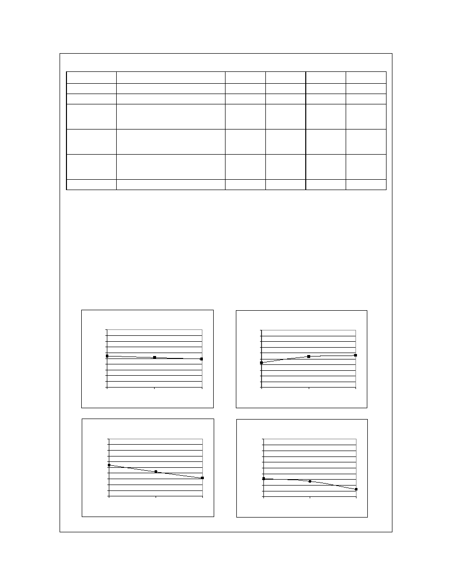
Performance Data
Symbol
Parameter
Min
Typ
Max
Units
f
Operating Frequency
1920
1980
MHz
Vcc1, Vcc2
Supply Voltage
3.0
3.4
4.2
V
Vref
Reference Voltage
Operating
Shutdown
2.7
0
2.85
3.1
0.5
V
V
Vmode
Bias Control Voltage
Low-Power
High-Power
1.8
0
2.0
3.0
0.5
V
V
Pout
Linear Output Power
High-Power
Low-Power
+27
+16
dBm
dBm
Tc
Case Operating Temperature
-30
+85
°C
RMPA2059 4x4 WCDMA PAM
Vcc=3.4V, Vref = 2.85V, Vmode=0V, Pout=27dBm
22.0
23.0
24.0
25.0
26.0
27.0
28.0
29.0
30.0
31.0
32.0
1920
1950
1980
Frequency (MHz )
Ga
i
n
(
d
B
)
RMPA2059 4x4 WCDMA PAM
Vcc=3.4V, Vref = 2.85V, Vmode=0V, Pout=27dBm
35.0
36.0
37.0
38.0
39.0
40.0
41.0
42.0
43.0
44.0
45.0
1920
1950
1980
Frequency (MHz )
PA
E (
%
)
RMPA2059 4x4 WCDMA PAM
Vcc=3.4V, Vref = 2.85V, Vmode=0V, Pout=27dBm
-50.0
-48.0
-46.0
-44.0
-42.0
-40.0
-38.0
-36.0
-34.0
-32.0
-30.0
1920
1950
1980
Frequency (MHz )
ACLR1
(
d
Bc
)
RMPA2059 4x4 WCDMA PAM
Vcc=3.4V, Vref = 2.85V, Vmode=0V, Pout=27dBm
-60.0
-58.0
-56.0
-54.0
-52.0
-50.0
-48.0
-46.0
-44.0
-42.0
-40.0
1920
1950
1980
Frequency (MHz)
ACLR2
(
d
Bc
)

RM
P
A
2
0
5
9
WC
DM
A Po
we
r
Ed
g
e
TM
P
o
we
r
A
m
p
lif
ier
M
o
d
u
le
©2005 Fairchild Semiconductor Corporation
4
www.fairchildsemi.com
RMPA2059 Rev. F
3
6
5
6
5
1
2
Evaluation Board Layout
Materials List
Evaluation Board Schematic
Qty
Item No.
Part Number
Description
Vendor
1
1
G657553-1 V2
PC Board
Fairchild
2
2
#142-0701-841
SMA Connector
Johnson
3
3
#2340-5211TN
Terminals
3M
Ref
4
G657637
Assembly, RMPA2059
Fairchild
3
5
GRM39XR102KS0V
1000pF Capacitor (0603)
Murata
3
5 (Alt)
ECJ-1V81H102K
1000pF Capacitor (0603)
Panasonic
2
6
C3216X5R1A335M
3.3µF Capacitor (1206)
TDK
1
7
GRM39YSV104Z16V
0.1µF Capacitor (0603)
Murata
1
7 (Alt)
ECJ-1VB1CID4K
0.1µF Capacitor (0603)
Panasonic
A/R
8
SN63
Solder Paste
Indium Corp.
A/R
9
SN96
Solder Paste
Indium Corp
2
10
8
3, 6, 7, 9
VCC2
(PACKAGE BASE)
50
Ohm
TRL
50
SMA2
RF
O
UT
SMA1
RF IN
Ohm
TRL
3.3 µF
VREF
3.3 µF
1000 pF
1000 pF
1000 pF
0.1 µF
4
VM
O
DE
11
5
VCC1
1
2059
YWWXX
RM
P
A
2
0
5
9
WC
DM
A Po
we
r
Ed
g
e
TM
P
o
we
r
A
m
p
lif
ier
M
o
d
u
le
©2005 Fairchild Semiconductor Corporation
5
www.fairchildsemi.com
RMPA2059 Rev. F
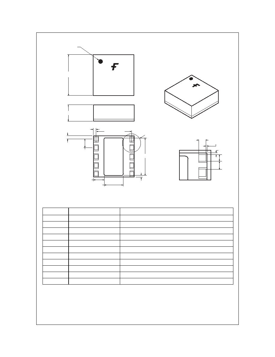
Package Outline
Signal Descriptions
Pin #
Signal Name
Description
1
Vcc1
Reference Voltage
2
RF In
High Power/Low Power Mode Control
3
GND
Ground
4
Vmode
RF Input Signal
5
Vref
Supply Voltage to Input Stage
6
GND
Ground
7
GND
Ground
8
RF Out
RF Output Signal
9
GND
Ground
10
Vcc2
Supply Voltage to Output Stage
11
GND
Paddle Ground
1
I/O 1 INDICATOR
TOP VIEW
FRONT VIEW
BOTTOM VIEW
DETAIL A. TYP.
(4.00mm
1.60mm MAX.
.30mm TYP.
.18mm
3.65mm
.85mm TYP.
.25mm TYP.
1.08mm
1.84mm
3.50mm TYP.
See Detail A
) SQUARE
+.100
.050
2
3
4
5
10
9
8
7
6
11
1
2
.40mm
.10mm
.10mm
.40mm
.45mm
2059
YWWXX
2059
YWWXX