 | ÐлекÑÑоннÑй компоненÑ: RMPA2271 | СкаÑаÑÑ:  PDF PDF  ZIP ZIP |
Äîêóìåíòàöèÿ è îïèñàíèÿ www.docs.chipfind.ru
©2005 Fairchild Semiconductor Corporation
1
www.fairchildsemi.com
May 2005
RMPA2271 Rev. B
RMP
A2271 WCDMA/UMTS P
o
wer Edg
eTM P
o
wer Amplifier Module with Integrated P
o
wer Detector
PRELIMINARY
RMPA2271
WCDMA/UMTS Power EdgeTM Power Amplifier
Module with Integrated Power Detector
Features
Temperature compensated, integrated power detector with
>20dB dynamic range
41% WCDMA efficiency at +28dBm average output power
19201980MHz
Meets UMTS/WCDMA and HSDPA performance
requirements
Compact Lead-free compliant LCC package
(3.0 x 3.0 x 1.0 mm nominal)
Single positive-supply operation and low power and
shutdown modes
Low Vref (2.85V) compatible with advanced handset
chipsets
Internally matched to 50
and DC blocked RF
input/output
General Description
The RMPA2271 Power Amplifier Module (PAM) is Fairchild's
latest innovation in 50
matched, surface mount modules
targeting WCDMA/UMTS applications. Answering the call for
integrated Power Detection, the RMPA2271 offers the ability to
measure power output over a 20dB range. This feature
eliminates the need of an external power detector and lossy
directional coupler, improving system perfomance and reducing
overall cost. Simple two-state Vmode control is all that is
needed to change the PA optimization from high power to low
power mode to minimize current usage. The 3 x 3 x 1.0mm LCC
package fits into the tightest spaces available on handset
boards and is footprint compatible with existing 3 x 3mm LCC
power amplifiers. The multi-stage GaAs Microwave Monolithic
Integrated Circuit (MMIC) is manufactured using Fairchild's
InGaP Heterojunction Bipolar Transistor (HBT) process.
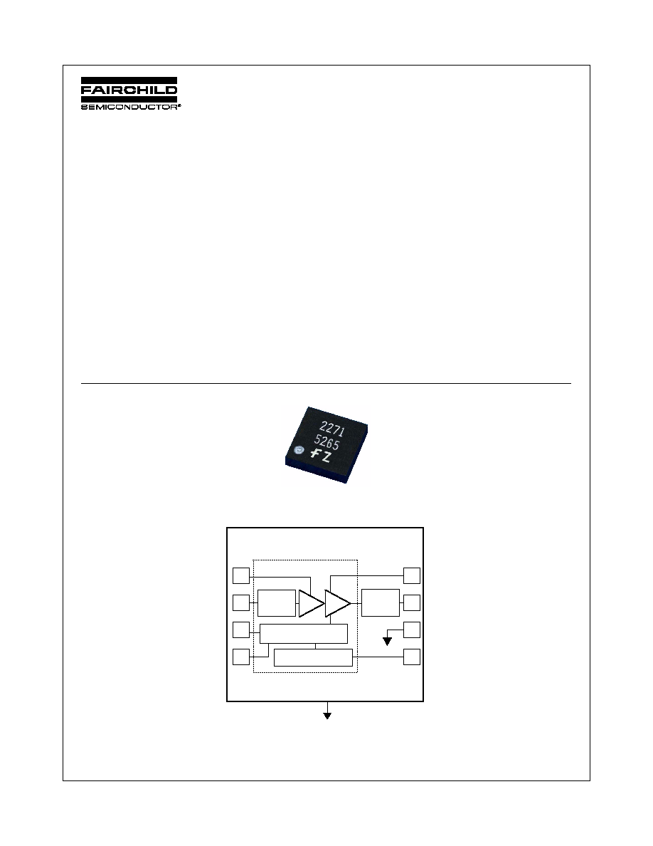
Device
Functional Block Diagram
4
3
2
1
8
7
6
5
DC Bias Control
4
3
2
1
8
7
6
5
Vcc2
RF OUT
GND
Vref
RF IN
Vcc1
MMIC
Input
Match
Output
Match
Vmode
Pdet
Power Detector

2
www.fairchildsemi.com
RMPA2271 Rev. B
RMP
A2271 WCDMA/UMTS P
o
wer Edg
eTM P
o
wer Amplifier Module with Integrated P
o
wer Detector
PRELIMINARY
Absolute Ratings
1
Note:
1. No permanent damage with only one parameter set at extreme limit. Other parameters set to typical values.
Electrical Characteristics (1920 to 1980 MHz)
1
Notes:
1. All parameters met at T
C
= +25°C, V
CC
= +3.4V, V
ref
= 2.85V and load VSWR
1.2:1, unless otherwise noted.
Symbol
Parameter
Ratings
Units
V
CC1
, V
CC2
Supply Voltages
5.0
V
V
ref
Reference Voltage
2.6 to 3.5
V
V
mode
Power Control Voltage
3.5
V
P
IN
RF Input Power
+10
dBm
T
STG
Storage Temperature
-55 to +150
°C
Symbol
Parameter
Min
Typ
Max
Units
Comments
f
Operating Frequency
1920
1980
MHz
WCDMA Operation
Gp
Power Gain
27
dB
Po = +28dBm, Vmode = 0V
26
dB
Po = +16dBm, Vmode
2.0V
Po
Linear Output Power
28
dBm
Vmode = 0V
16
dBm
Vmode
2.0V
PAEd
PAEd (digital) @ +28dBm
41
%
Vmode = 0V
PAEd (digital) @ +16dBm
9
%
Vmode
2.0V
PAEd (digital) @ +16dBm
25
%
Vmode
2.0V, Vcc = 1.4V
Itot
High Power Total Current
450
mA
Po = +28dBm, Vmode = 0V
Low Power Total Current
130
mA
Po = +16dBm, Vmode
2.0V
P
det
Detector Output
1.4
V
Po = +28dBm, Vmode
=
0V
0.3
V
Po = +16dBm, Vmode
2.0V
Adjacent Channel Leakage
Ratio
WCDMA Modulation 3GPP
3.2 03-00 DPCCH+1 DCDCH
ACLR1
±5.00MHz Offset
19201980MHz
-40
dBc
Po = +28dBm, Vmode = 0V
-42
dBc
Po = +16dBm, Vmode
2.0V
ACLR2
±10.00MHz Offset
19201980MHz
-54
dBc
Po = +28dBm, Vmode = 0V
-66
dBc
Po = +16dBm, Vmode
2.0V
General Characteristics
VSWR
Input Impedance
2.0:1
NF
Noise Figure
4
dB
Rx No
Receive Band Noise Power
-142
dBm/Hz Po
+28dBm, 2110 to 2170MHz
2fo 5fo
Harmonic Suppression
3
-50
dBc
Po
+28dBm
S
Spurious Outputs
2, 3
-60
dBc
Load VSWR
5.0:1
Ruggedness with Load
Mismatch
3
10:1
No permanent damage
Tc
Case Operating Temperature
-30
85
°C
DC Characteristics
Iccq
Quiescent Current
50
mA
Vmode
2.0V
Iref
Reference Current
7
mA
Po
+28dBm
Icc(off)
Shutdown Leakage Current
1
5
µA
No applied RF signal

3
www.fairchildsemi.com
RMPA2271 Rev. B
RMP
A2271 WCDMA/UMTS P
o
wer Edg
eTM P
o
wer Amplifier Module with Integrated P
o
wer Detector
PRELIMINARY
Typical Characteristics
Frequency and Temperature dependency
Power Detector dependency
RMPA2271
3x3
WCDMA
PAM
with
Power
Detector
Vcc=3.4V, Vref=2.85V, Vmode=0V, Pout=28dBm
RMPA2271
3x3
WCDMA
PAM
with
Power
Detector
Vcc=3.4V, Vref=2.85V, Vmode=0V, Pout=28dBm
RMPA2271
3x3
WCDMA
PAM
with
Power
Detector
Vcc=3.4V, Vref=2.85V, Vmode=0V, Pout=28dBm
RMPA2271
3x3
WCDMA
PAM
with
Power
Detector
Vcc=3.4V, Vref=2.85V, Vmode=0V, Pout=28dBm
22
23
24
25
26
27
28
29
30
31
32
1920
1950
1980
Frequency (MHz)
Ga
i
n
(d
B
)
T=25
°C
T=85
°C
T=- 30
°C
35
36
37
38
39
40
41
42
43
44
45
1920
1950
1980
Frequency (MHz)
PA
E
(
%
)
T=25
°
C
T=85
°
C
T=-30
°
C
-50
-48
-46
-44
-42
-40
-38
-36
-34
-32
-30
1920
1950
1980
Frequency (MHz)
ACL
R1
(
d
Bc
)
T=25
°C
T=85
°C
T= -30
°C
-60
-58
-56
-54
-52
-50
-48
-46
-44
-42
-40
1920
1950
1980
Frequency (MHz)
ACL
R2
(
d
Bc
)
T=25
°C
T=85
°C
T= -30
°C
0
0.2
0.4
0.6
0.8
1
1.2
1.4
1.6
1.8
-10
-5
0
5
10
15
20
25
30
Pout (dBm )
Pd
e
t
(
V
d
c
)
V ref=2.75V
V ref=2.85V
V ref=2.95V
0
0.2
0.4
0.6
0.8
1
1.2
1.4
1.6
1.8
-10
-5
0
5
10
15
20
25
30
Pout (dBm )
Pd
e
t
(
V
d
c
)
T=25
°C
T= 85
°C
T=-30
°C
RMPA2271
3x3
WCDMA
PAM
with
Power
Detector
Vcc=3.4V, Vmode=0V, Freq=1950MHz, Temp=25
°C
RMPA2271
3x3
WCDMA
PAM
with
Power
Detector
Vcc=3.4V, Vmode=0V, Freq=1950MHz, Vref=2.85V
4
www.fairchildsemi.com
RMPA2271 Rev. B
RMP
A2271 WCDMA/UMTS P
o
wer Edg
eTM P
o
wer Amplifier Module with Integrated P
o
wer Detector
PRELIMINARY
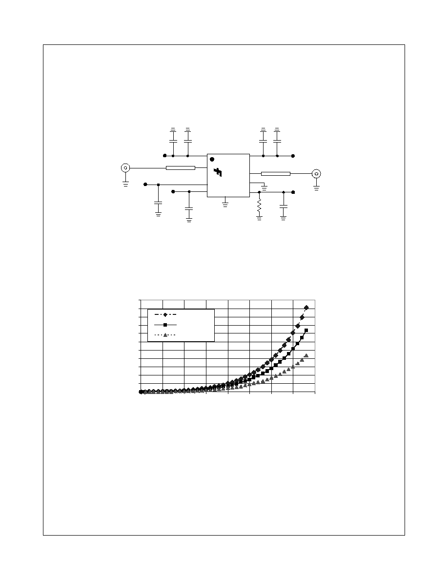
Application Note
Due to the varying amplitude envelope of WCDMA signal, a filter is required at the Pdet pin in order to minimize the ripple noise of the
detector output voltage (Pdet). RMPA2271 has no integrated filter for the Pdet pin. Therefore, an external low-pass filter, comprising a
shunt resistor (R) and a shunt capacitor (C), is required to detect the WCDMA signal properly. The filter bandwidth is determined by
the RC time constant of the filter, and can be reduced by increasing the values of the resistor and/or capacitor. A narrower filter band-
width has the advantage of lower voltage ripple noise, but it comes at the expense of increased response time. A tradeoff needs to be
made between the ripple noise and response time for the optimal system performance.
The detector output voltage (Pdet) range can be adjusted by the value of the external shunt resistor (R). The following figure shows
the dependence of Pdet voltage as a function of R. The maximum Pdet voltage can be increased by raising the value of R. This pro-
vides the added flexibility to handset designers to change the detector range to meet the system requirements.
It is recommended that the value of the resistor R is first determined depending on the desired detector output voltage range. Then
the value of the shunt capacitor C is selected for the required detector output voltage ripple level, and response time.
2
8
7
6
5
SMA1
RF IN
Vcc2
Pdet
(package
base)
50 ohm
TRL
50 ohm
TRL
3.3
µF
Vref
3.3
µF
1000 pF
1000 pF
1000 pF
0.1
µF
3
Vmode
C
R
9
4
SMA2
RF OUT
1
Vcc1
2271
XYTT
Z
0.0
0.2
0.4
0.6
0.8
1.0
1.2
1.4
1.6
1.8
2.0
-10
-5
0
5
10
15
20
25
30
Pout (dBm)
Pd
e
t
(
V
d
c
)
R=9.1k Ohm
R=5.1k Ohm
R=2.4k Ohm
RMPA2271
3x3
WCDMA
PAM
with
Power
Detector
Vcc=3.4V, Vref=2.85V, Vmode=0V, Freq=1950MHz, Temp=25
°C

5
www.fairchildsemi.com
RMPA2271 Rev. B
RMP
A2271 WCDMA/UMTS P
o
wer Edg
eTM P
o
wer Amplifier Module with Integrated P
o
wer Detector
PRELIMINARY
Efficiency Improvement Applications
In addition to high-power/low-power bias modes, the efficiency of the PA module can be significantly increased at backed-off RF
power levels by dynamically varying the supply voltage (Vcc) applied to the amplifier. Since mobile handsets and power amplifiers fre-
quently operate at 10-20 dB back-off, or more, from maximum rated linear power, battery life is highly dependent on the DC power
consumed at antenna power levels in the range of 0 to +16dBm. The reduced demand on transmitted RF power allows the PA supply
voltage to be reduced for improved efficiency, while still meeting linearity requirements for WCDMA modulation with excellent margin.
High-efficiency DC-DC converters are now available to implement switched-voltage operation.
With the PA module in low-power mode (Vmode = +2.0V) at+16dBm output power and supply voltages reduced from 3.4V nominal
down to 1.2V, power-added efficiency is more than doubled from 9.5 percent to nearly 25 percent (Vcc = 1.2V) while maintaining a
typical ACLR1 of 40dBc and ACLR2 of less than 54dBc. Operation at even lower levels of Vcc supply voltage are possible with a
further restriction on the maximum RF output power.
Recommended Operating Conditions
DC Turn On Sequence:
1. Vcc1 = Vcc2 = 3.4V (typical)
2. Vref = 2.85V (typical)
3. High-Power: Vmode = 0V (Pout > 16dBm)
Low-Power: Vmode = 2.0V (Pout < 16dBm)
Symbol
Parameter
Min
Typ
Max
Units
f
Operating Frequency
1920
1980
MHz
Vcc1, Vcc2
Supply Voltage
3.0
3.4
4.2
V
Vref
Reference Voltage
(Operating)
(Shutdown)
2.7
0
2.85
3.1
0.5
V
V
Vmode
Bias Control Voltage
(Low-Power)
(High-Power)
1.8
0
2.0
3.0
0.5
V
V
Pout
Linear Output Power
(High-Power)
(Low-Power)
+28
+16
dBm
dBm
Tc
Case Operating Temperature
-30
+85
°C