
www.fairchildsemi.com
REV. 1.0.2 10/25/00
Features
∑ Four user-selectable filtering and transformation
functions:
≠ Triple dot product (3 x 3) matrix multiply
≠ Cascadeable 9-tap systolic FIR filter
≠ Cascadeable 3 x 3-pixel image convolver
≠ Cascadeable 4 x 2-pixel image convolver
∑ 50 MHz (20ns) pipelined throughput
∑ 12-bit input and output data, 10-bit coefficients
∑ 6-bit cascade input and output ports in all filter modes
∑ Onboard coefficient storage, with three-cycle updating of
all nine coefficients
Applications
∑ Image filtering and manipulation
∑ Video effects generation
∑ Video standards conversion and encoding/decoding
∑ Three-dimensional image manipulation
∑ Medical image processing
∑ Edge detection for object recognition
∑ FIR filtering for communications systems
Description
The TMC2250A is a flexible high-performance nine-multiplier
array VLSI circuit which can execute a cascadeable 9-tap
FIR filter, a cascadeable 4 x 2 or 3 x 3-pixel image convolu-
tion, or a 3 x 3 color space conversion. All configurations
offer throughput at up to the maximum guaranteed 50 MHz
clock rate with 12-bit data and 10-bit coefficients. All inputs
and outputs are registered on the rising edges of the clock.
The 3 x 3 matrix multiply or color conversion configuration
can perform video standard conversion (YIQ or YUV to
RGB, etc.) or three-dimensional perspective translation at
real-time video rates.
The 9-tap FIR filter configuration, useful in Video, Telecom-
munications, and Signal Processing, features a 16-bit cascade
input to allow construction of longer filters.
The cascadeable 3 x 3 and 4 x 2-pixel image convolver func-
tions allow the user to perform numerous image processing
functions, including static filters and edge detectors. The 16-bit
cascade input port facilitates two-chip 50 MHz cubic convo-
lution (4 x 4-pixel kernel).
The TMC2250A is fabricated in a sub-micron CMOS process
and operates at clock speeds of up to 50 MHz over the full
commercial (0∞C to 70∞C) temperature and supply voltage
ranges. It is available in 120-pin Plastic Pin Grid Array
(PPGA) packages, 120-lead Ceramic Pin Grid Array pack-
age (CPGA), 120-lead PQFP to PPGA package (MPGA) and
120-lead Plastic Quad FlatPack (PQFP). All input and output
signals are TTL compatible.
TMC2250A
Matrix Multiplier
12 x 10 bit, 50 MHz

PRODUCT SPECIFICATION
TMC2250A
2
REV. 1.0.2 10/25/00
Functional Description
The TMC2250A is a nine-multiplier array with the internal bus
structure and summing adders needed to implement a 3 x 3
matrix multiplier (triple dot product) a cascadeable 9-tap FIR
filter, a 3 x 3-pixel convolver, or a 4 x 2-pixel convolver all in
one monolithic circuit. With a 50MHz guaranteed maximum
clock rate, this device offers video and imaging system
designers a single-chip solution to numerous common image
and signal-processing problems.
The three data input ports (A, B, C) accept 12-bit two's com-
plement integer data, which is also the format for the output
ports (X, Y, Z) in the matrix multiply mode (Mode 00). In the
filter configurations (Modes 01, 10, and 11) the cascade ports
assume 12-bit integer, 4-bit fractional two's complement data
on both input and output. The coefficient input ports (KA,
KB, KC) are always 10-bit two's complement fractional.
Table 1 details the bit weighting of the input and output data
in all configurations.
Operating Modes
The TMC2250A can implement four different digital filter
architectures. Upon selection of the desired function by the
user (MODE
1-0
), the device reconfigures its internal data
paths and input and output buses appropriately. The output
ports (XC, YC and ZC) are configured in all filter modes a
16-bit Cascade In and Cascade Out ports so that multiple
devices can be connected to build larger filters. These modes
are described individually below. The I/O function configu-
rations for all four modes are shown in Table 1.
Definitions
The calculations performed by the TMC2250A in each mode
are also shown below, utilizing the following notation:
A(1), B(5), C(2), CASIN(3)
Indicates the data word presented to that input port during
the specified clock rising edge(x). Applies to all input ports
A
11-0
, B
11-0
, C
11-0
, and CASIN
15-0
.
KA1(1), KB3(4)
Indicates coefficient data stored in the specified one of the
nine onboard coefficient registers KA1 through KC3, as
shown in the block diagram for that mode, input during or
before the specified clock rising edge (x).
X(1), Y(4), Z(6), CASOUT (6)
Indicated data available at that output port t
DO
after that
specified clock rising edge (x). Applies to all output ports
X
11-0
, Y
11-0
, Z
11-0
, and CASOUT
15-0
.
Numeric Format
Table 2 shows the binary weightings of the input and output
ports of the TMC2250A. Although the internal sums of prod-
ucts could grow to 23 bits, in the matrix multiply mode
(Mode 00) the outputs X, Y and Z are rounded to yield 12-bit
integer words. Thus the output format is identical to the input
data format. In the filter configurations (Modes 01, 10, and
11) the cascade output is always half-LSB rounded to 16
bits, specifically 12 integer bits and 4 fractional guard bits,
with no overflow "headroom". The user is of course free to
half-LSB round the output word to any size less than 16 bits
by forcing a 1 into the bit position of the cascade input
immediately below the desired LSB. In all modes, bit
weighting is easily adjusted if desired by applying the same
scaling correction factor to both input and output data words.
If the coefficients are rescaled, the relative weightings of the
CASIN and CASOUT ports will differ accordingly.
Data Overflow
As shown in Table 2, the TMC2250A's matched input and
output data formats accommodate 0dB (unity) gain. There-
fore, the user must be aware of input conditions that could
lead to numeric overflow. Maximum input data and coeffi-
cient word sizes must be taken into account with the specific
algorithm performed to ensure that no overflow occurs.
Table 1. Data Port Formatting by Mode
Mode
Inputs
Inputs/Output
Outputs
A
11-0
B
11-0
C
11-0
KA
9-0
KB
9-0
KC9-0
XC
11-0
YC
11-8
Y
7-4
YC3-0
ZC
11-0
00
A
11-0
B
11-0
C
11-0
KA
9-0
KB
9-0
KC9-0
X
11-0
Y
11-8
Y
7-4
Y
3-0
Z
11-0
01
A
11-0
B
11-0
NC
KA
9-0
KB
9-0
KC9-0
CASIN
15-4
CASIN
3-0
NC
CASOUT
3-0
CASOUT
15-4
10
A
11-0
B
11-0
C
11-0
KA
9-0
KB
9-0
KC9-0
CASIN
15-4
CASIN
3-0
NC
CASOUT
3-0
CASOUT
15-4
11
A
11-0
B
11-0
NC
KA
9-0
KB
9-0
KC9-0
CASIN
15-4
CASIN
3-0
NC
CASOUT
3-0
CASOUT
15-4

TMC2250A
PRODUCT SPECIFICATION
REV. 1.0.2 10/25/00
3
Table 2. Bit Weightings for Input and Output Data Words
Note:
A minus sign indicates a two's complement sign bit.
Bit Weights
2
11
2
10
2
9
2
8
2
7
2
6
2
5
2
4
2
3
2
2
2
1
2
0
. 2
-1
2
-2
2
-3
2
-4
2
-5
2
-6
2
-7
2
-8
2
-9
Inputs
All Modes
Data A, B, C
-I
11
I
10
I
9
I
8
I
7
I
6
I
5
I
4
I
3
I
2
I
1
I
0
.
Coefficients
KA, KB, KC
-K
9
. K
8
K
7
K
6
K
5
K
4
K
3
K
2
K
1
K
0
Modes 01,
10, 11 CASIN
-CI
15
CI
14
CI
13
CI
12
CI
11
CI
10
CI
9
CI
8
CI
7
CI
6
CI
5
CI
4
. CI
3
CI
2
CI
1
CI
0
Internal Sum
X
20
X
19
X
18
X
17
X
16
X
15
X
14
X
13
X
12
X
11
X
10
X
9
. X
8
X
7
X
6
X
5
X
4
X
3
X
2
X
1
X
0
Outputs
Mode 00
X, Y, Z
-O
11
O
10
O
9
O
8
O
7
O
6
O
5
O
4
O
3
O
2
O
1
O
0
.
Modes 01,
10, 11
CASOUT
-
CO
15
CO
1
4
CO
1
3
CO
1
2
CO
1
1
CO
1
0
CO
9
CO
8
CO
7
CO
6
CO
5
CO
4
. CO
3
CO
2
CO
1
CO
0
PRODUCT SPECIFICATION
TMC2250A
4
REV. 1.0.2 10/25/00
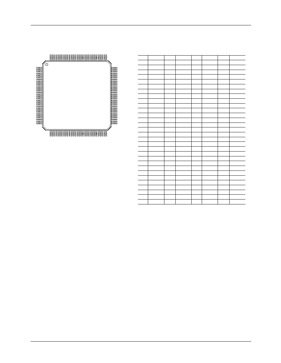
Pin Assignments
120 Pin Plastic Quad Flat Pack (MQFP), KE Package
XC6
XC5
XC4
XC3
XC2
XC1
XC0
GND
YC11
YC10
YC9
VDD
YC8
Y7
Y6
GND
Y5
Y4
YC0
VDD
YC1
YC2
YC3
GND
ZC0
ZC1
ZC2
ZC3
ZC4
ZC5
1
30
120
91
31
60
1
2
3
4
5
6
7
8
9
10
11
12
13
14
15
16
17
18
19
20
21
22
23
24
25
26
27
28
29
30
90
61
ZC6
ZC7
ZC8
GND
ZC9
ZC10
ZC11
KC0
KC1
KC2
KC3
GND
KC4
KC5
KC6
VDD
KC7
KC8
KC9
KB0
KB1
KB2
KB3
KB4
KB5
KB6
KB7
KB8
KB9
KA0
31
32
33
34
35
36
37
38
39
40
41
42
43
44
45
46
47
48
49
50
51
52
53
54
55
56
57
58
59
60
Pin
Name
Pin
Name
KA1
KA2
KA3
KA4
KA5
KA6
KA7
KA8
KA9
CWE1
CWE0
GND
A0
A1
A2
A3
A4
A5
A6
A7
A8
A9
A10
A11
B0
B1
B2
CLK
B3
B4
61
62
63
64
65
66
67
68
69
70
71
72
73
74
75
76
77
78
79
80
81
82
83
84
85
86
87
88
89
90
B5
B6
B7
B8
B9
B10
B11
C0
C1
C2
C3
VDD
C4
C5
C6
GND
C7
C8
C9
C10
C11
MODE1
MODE0
GND
XC11
XC10
XC9
VDD
XC8
XC7
91
92
93
94
95
96
97
98
99
100
101
102
103
104
105
106
107
108
109
110
111
112
113
114
115
116
117
118
119
120
Pin
Name
Pin
Name
TMC2250A
PRODUCT SPECIFICATION
REV. 1.0.2 10/25/00
5
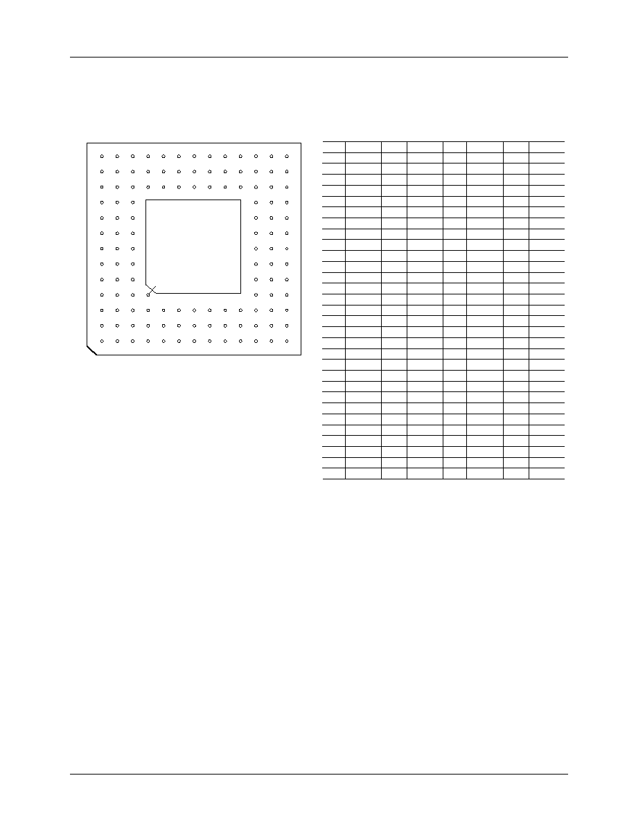
Pin Assignments
(continued)
120 Pin Plastic Pin Grid Array, H5 Package and 120 Pin Ceramic Pin Grid Array, G1 Package and
120 Pin Plastic Quad Flatpack to 120-Pin Pin Grid Array (MPGA)
B
A
D
E
F
G
H
J
K
L
M
N
C
1
2
3
4
5
6
7
8
9
10
11
12
13
Top View
Cavity Up
KEY
XC7
XC9
XC10
MODE0
C11
C8
C7
C5
C3
C1
B10
B7
B4
XC4
XC5
XC8
XC11
MODE1
C9
C6
C4
C2
B11
B9
B6
B2
XC1
XC2
XC6
VDD
A1
A2
A3
A4
A5
A6
A7
A8
A9
A10
A11
A12
A13
B1
B2
B3
B4
B5
B6
B7
B8
B9
B10
B11
B12
B13
C1
C2
C3
C4
GND
C10
GND
VDD
C0
B8
B5
B3
B1
YC11
XC0
XC0
CLK
B0
A10
YC9
YC10
GND
A11
A9
A8
Y7
YC8
VDD
A7
A6
A5
Y5
Y6
GND
C5
C6
C7
C8
C9
C10
C11
C12
C13
D1
D2
D3
D11
D12
D13
E1
E2
E3
E11
E12
E13
F1
F2
F3
F11
F12
F13
G1
G2
G3
Pin
Name
Pin
Name
A3
A2
A3
Y4
YC0
VDD
GND
A0
A1
YC1
YC2
GND
KA8
CWE1
CWE0
YC3
ZC0
ZC3
KA4
KA7
KA9
ZC1
ZC4
ZC6
GND
KC0
GND
VDD
KB0
KB4
G11
G12
G13
H1
H2
H3
H11
H12
H13
J1
J2
J3
J11
J12
J13
K1
K2
K3
K11
K12
K13
L1
L2
L3
L4
L5
L6
L7
L8
L9
KB8
KA1
KA5
KA6
ZC2
ZC7
ZC9
ZC11
KC2
KC4
KC6
KC9
KB2
KB5
KB9
KA2
KA3
ZC5
ZC8
ZC10
KC1
KC3
KC5
KC7
KC8
KB1
KB3
KB6
KB7
KA0
L10
L11
L12
L13
M1
M2
M3
M4
M5
M6
M7
M8
M9
M10
M11
M12
M13
N1
N2
N3
N4
N5
N6
N7
N8
N9
N10
N11
N12
N13
Pin
Name
Pin
Name