/home/web/htmldatasheet/RUSSIAN/html/fairchild/202514
www.fairchildsemi.com
REV. 1.1.8 10/31/00
Features
· Rectangular-to-Polar or Polar-to-Rectangular conversion
at guaranteed 40 MOPS pipelined throughput rate
· Polar data: 16-bit magnitude, 32-bit input/16-bit output
phase
· 16-bit user selectable two's complement or sign-and-
magnitude rectangular data formats
· Input register clock enables and asynchronous output
enables simplify interfacing
· User-configurable phase accumulator for waveform
synthesis and amplitude, frequency, or phase modulation
· Magnitude output data overflow flag (in Polar-to-
Rectangular mode)
· Low power consumption CMOS process
· Single +5V power supply
· Available in a 120-pin plastic pin grid array package
(PPGA), 120-pin ceramic pin grid array package (CPGA),
120-pin MQFP to PPGA (MPGA) package, and 120-pin
metric quad flatpack package (MQFP)
Applications
· Scan conversion (phased array to raster)
· Vector magnitude estimation
· Range and bearing derivation
· Spectral analysis
· Digital waveform synthesis, including quadrature
functions
· Digital modulation and demodulation
Description
The TMC2330A VLSI circuit converts bidirectionally
between Cartesian (real and imaginary) and Polar (magnitude
and phase) coordinates at up to 40 MOPS (Million Operations
Per Second).
In its Rectangular-to-Polar mode, the TMC2330A can extract
phase and magnitude information or backward "map" from a
rectangular raster display to a radial (e.g., range-and-azimuth)
data set.
The Polar-to-Rectangular mode executes direct digital waveform
synthesis and modulation. The TMC2330A greatly simplifies
real-time image-space conversion between the radially-generated
image scan data found in radar, sonar, and medical imaging
systems, and raster display formats.
All input and output data ports are registered, and a new trans-
formed data word pair is available at the output every clock
cycle. The user-configurable phase accumulator structure,
input clock enables, and asynchronous three-state output bus
enables simplify interfacing. All signals are TTL compatible.
Fabricated in a submicron CMOS process, the TMC2330A
operates at up to the 40 MHz maximum clock rate over the full
commercial (0 to 70°C) temperature and supply voltage ranges,
and is available in 120-pin plastic pin grid array, 120-pin
ceramic pin grid array, 120-pin metric quad flatpack to PPGA
package, and 120-pin metric quad flatpack packages.
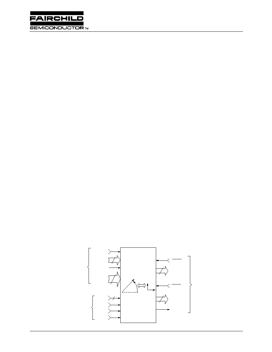
Logic Symbol
TMC2330A
DATA
INPUTS
YPIN
31-0
32
ACC
1-0
CONFIGURATION
CONTROLS
16
OEPY
PYOUT
15-0
OVF
RXOUT
15-0
DATA
OUTPUTS
ENXR
16
TCXY
RTP
CLK
OERX
ENYP
1-0
XRIN
15-0
2
16
TMC2330A
Coordinate Transformer
16 x 16 Bit, 40 MOPS
PRODUCT SPECIFICATION
TMC2330A
2
REV. 1.1.8 10/31/00
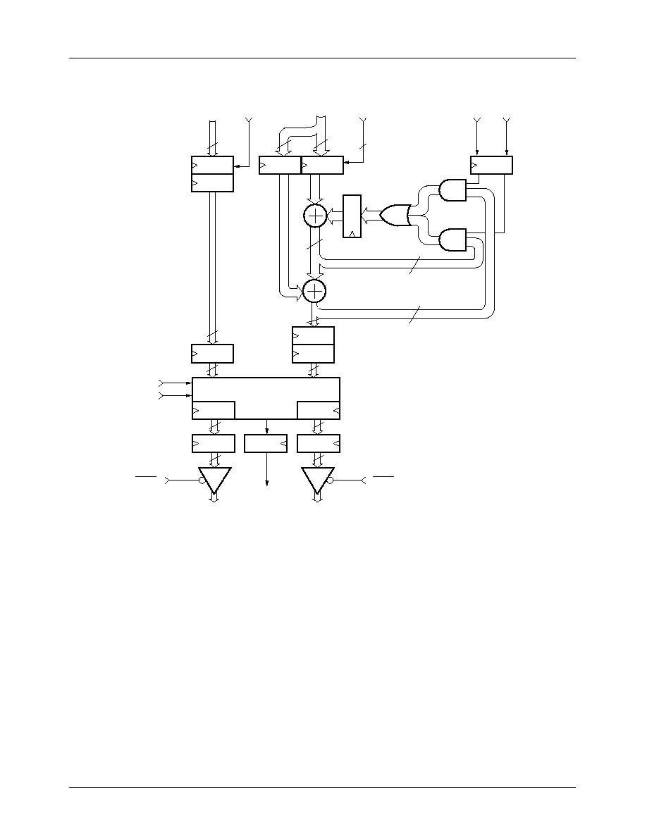
Block Diagram
1
XRIN
15-0
ENXR
16
2
AM
TCXY
3
4-21
22
22
22
4-21
16
16
16
16
16
OVF
PYOUT
15-0
OEPY
RXOUT
15-0
16
RPT
TRANSFORMATION PROCESS
16
2
3
16
OERX
ACC
1
ENYP
1-0
C
M
32
32
YPIN
31-0
2
ACC
0
32
32
32
FM
PM
32
32
32
Functional Description
The TMC2330A converts between Rectangular (Cartesian)
and Polar (Phase and Magnitude) coordinate data word pairs.
The user selects the numeric format and transformation to be
performed (Rectangular-To-Polar or Polar-To-Rectangular),
and the operation is performed on the data presented to the
inputs on the next clock. The transformed result is then
available at the outputs 22 clock cycles later, with new out-
put data available every 20ns with a 40 MHz clock. All input
and output data ports are registered, with input clock enables
and asynchronous high-impedance output enables to sim-
plify connections to system buses.
When executing a Rectangular-To-Polar conversion, the input
ports accept 16-bit Rectangular coordinate words, and the out-
put ports generate 16-bit magnitude and 16-bit phase data. The
user selects either two's complement or sign-and-magnitude
Cartesian data format. Polar magnitude data are always in
magnitude format only. Since the phase angle word is modulo
2
, it may be regarded as either unsigned or two's complement
format (Tables 1 and 2)
.
In Polar-To-Rectangular mode, the input ports accept 16-bit
Polar magnitude and 32-bit phase data, and the output ports
produce 16-bit Rectangular data words. Again, the user
selects between two's complement or sign-and-magnitude
Cartesian data format.
TMC2330A
PRODUCT SPECIFICATION
REV. 1.1.8 10/31/00
3
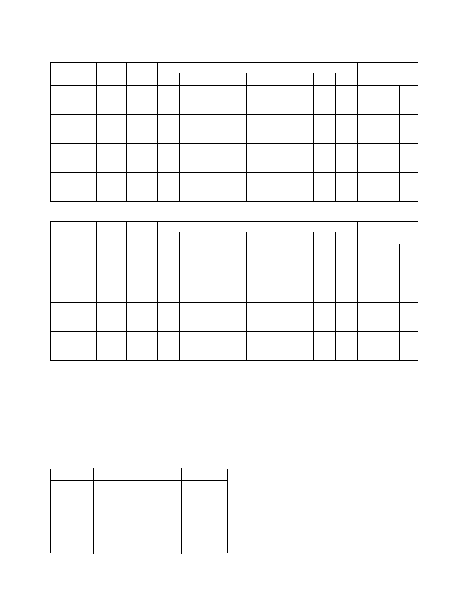
Table 1. Data Input/Output Formats--Integer Format
Table 2. Data Input/Output Formats--Fractional Format
Notes:
1. -2
15
denotes two's complement sign bit.
2. NS denotes negative sign, i.e., `1' negates the number.
3. ±2
0
denotes two's complement sign or highest magnitude bit since phase angles are modulo 2
and phase accumulator is
modulo 2
32
, this bit may be regarded as +
or -
.
4. All phase angles are in terms of
radians, hence notation "x
."
5. If A
CC
= 00, YPIN(15-0) are "don't cares."
6. Formats:
T = Two's Complement
S = Signed Magnitude
U = Unsigned
Port
RTP
TCXY
Bit #
Format
31
30
29
...
16
15
14
...
0
XRIN
XRIN
XRIN
0
1
1
X
0
1
2
15
NS
2
15
2
14
2
14
2
14
...
...
...
2
0
2
0
2
0
U
S
T
YPIN
YPIN
YPIN
0
1
1
X
0
1
±2
0
NS
2
15
2
-1
2
14
2
14
2
-2
2
13
2
13
...
...
2
-15
2
0
2
0
2
-16
2
-17
...
2
-31
(x
)T/U
S
T
RXOUT
RXOUT
RXOUT
0
0
1
0
1
X
NS
2
15
2
15
2
14
2
14
2
14
2
0
2
0
2
0
S
T
U
PYOUT
PYOUT
PYOUT
0
0
1
0
1
X
NS
2
15
±2
0
2
14
2
14
2
-1
2
0
2
0
2
-15
(x
)T/U
S
T
Port
RTP
TCXY
Bit #
Format
31
30
29
...
16
15
14
...
0
XRIN
XRIN
XRIN
0
1
1
X
0
1
2
0
NS
2
0
2
-1
2
-1
2
-1
...
...
...
2
-15
2
-15
2
-15
U
S
T
YPIN
YPIN
YPIN
0
1
1
X
0
1
±2
0
NS
-2
0
2
-1
2
-1
2
-1
2
-2
2
-2
2
-2
...
...
...
2
-15
2
-15
2
-15
2
-16
2
-17
...
2
-31
(x
)T/U
S
T
RXOUT
RXOUT
RXOUT
0
0
1
0
1
X
NS
2
0
2
0
2
-1
2
-1
2
-1
...
...
...
2
-15
2
-15
2
-15
S
T
U
PYOUT
PYOUT
PYOUT
0
0
1
0
1
X
NS
2
0
±2
0
2
-1
2
-1
2
-1
...
...
...
2
-15
2
-15
2
-15
(x
)T/U
S
T
HEX
U
T
S
FFFF
...
8001
8000
7FFF
...
0001
0000
65535
...
32769
32768
32767
...
1
0
1
...
-32767
-32768
32767
...
1
0
-32767
...
-1
0
32767
...
1
0
PRODUCT SPECIFICATION
TMC2330A
4
REV. 1.1.8 10/31/00
Static Control Inputs
The controls RTP and TCXY determine the transformation
mode and the assumed numeric format of the Rectangular
data. The user must exercise caution when changing either of
these controls, as the new transformed results will not be
seen at the outputs until the entire internal pipe (22 clocks)
has been flushed. Thus, these controls are considered static.
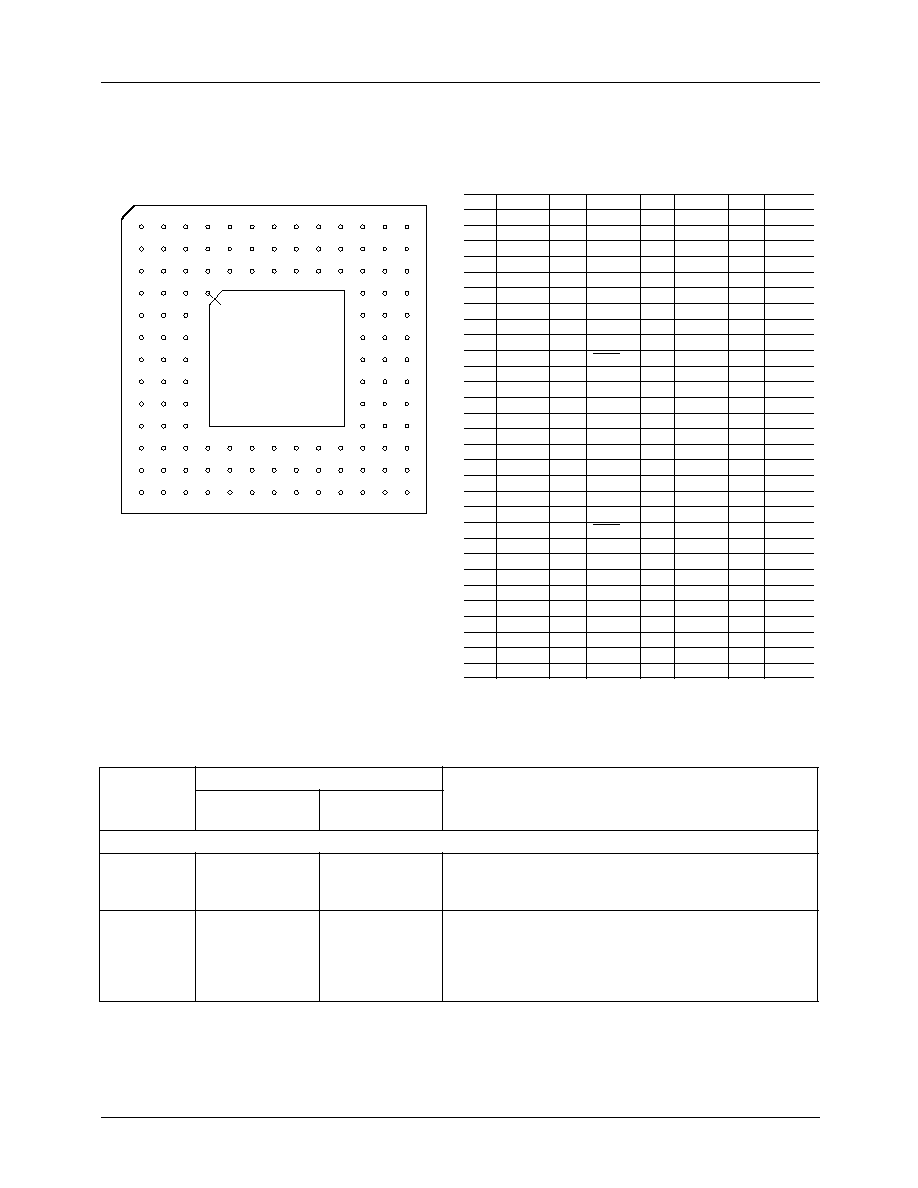
Pin Assignments
120-Pin MQFP
VDD
PYOUT4
PYOUT3
GND
PYOUT2
PYOUT1
PYOUT0
VDD
OEPY
GND
RTP
CLK
GND
TCXY
ENPY
GND
ENPY1
ACC0
ACC1
VDD
YPIN0
YPIN1
YPIN2
YPIN3
YPIN4
YPIN5
YPIN6
GND
YPIN7
YPIN8
1
2
3
4
5
6
7
8
9
10
11
12
13
14
15
16
17
18
19
20
21
22
23
24
25
26
27
28
29
30
GND
YPIN9
YPIN10
VDD
YPIN11
YPIN12
YPIN13
YPIN14
YPIN15
YPIN16
YPIN17
VDD
YPIN18
YPIN19
YPIN20
GND
YPIN21
YPIN22
YPIN23
VDD
YPIN24
YPIN25
YPIN26
YPIN27
YPIN28
YPIN29
YPIN30
YPIN31
ENXR
XRIN0
31
32
33
34
35
36
37
38
39
40
41
42
43
44
45
46
47
48
49
50
51
52
53
54
55
56
57
58
59
60
Pin 1
Pin
Name
Pin
Name
VDD
XRIN1
XRIN2
GND
XRIN3
XRIN4
XRIN5
GND
XRIN6
XRIN7
XRIN8
XRIN9
XRIN10
XRIN11
XRIN12
GND
XRIN13
XRIN14
XRIN15
VDD
OERX
GND
RXOUT15
VDD
RXOUT14
RXOUT13
RXOUT12
GND
RXOUT11
RXOUT10
61
62
63
64
65
66
67
68
69
70
71
72
73
74
75
76
77
78
79
80
81
82
83
84
85
86
87
88
89
90
VDD
RXOUT9
RXOUT8
GND
RXOUT7
RXOUT6
RXOUT5
GND
RXOUT4
RXOUT3
RXOUT2
VDD
RXOUT1
RXOUT0
OVF
GND
PYOUT15
PYOUT14
PYOUT13
VDD
PYOUT12
PYOUT11
PYOUT10
GND
PYOUT9
PYOUT8
PYOUT7
GND
PYOUT6
PYOUT5
91
92
93
94
95
96
97
98
99
100
101
102
103
104
105
106
107
108
109
110
111
112
113
114
115
116
117
118
119
120
Pin
Name
Pin
Name
TMC2330A
PRODUCT SPECIFICATION
REV. 1.1.8 10/31/00
5
Pin Assignments
(continued)
120-Pin PPGA, H5 Package and 120-Pin CPGA, G1 Package and 120-Pin Metric Quad Flatpack to
120-Pin Plastic Pin Array, H6 Package
Pin Descriptions
Pin Name
Pin Number
Description
MQFP
CPGA/PPGA/
MPGA
Power, Ground and Clock
V
DD
1, 8, 20, 34, 42,
50, 61, 80, 84, 91,
102, 110
C3, E3, H3, L4, L6,
L8, L11, F11, E11,
C11, C8, C6
The TMC2330A operates from a single +5V supply. All
power and ground pins must be connected.
GND
4, 10, 13, 16, 28,
31, 46, 64, 68, 76,
82, 88, 94, 98,
106, 114, 118
D3, E2, F2, G3,
K3, L3, L7, K11,
J11, G11, E12,
D11, C10, C9, C7,
C5, C4
Ground
PYOUT5
PYOUT7
PYOUT8
PYOUT10
PYOUT12
PYOUT14
PYOUT15
RXOUT0
RXOUT2
RXOUT4
RXOUT6
RXOUT8
RXOUT10
PYOUT3
PYOUT4
PYOUT6
PYOUT9
PYOUT11
PYOUT13
OVF
RXOUT1
RXOUT3
RXOUT5
RXOUT7
RXOUT9
RXOUT12
PYOUT1
PYOUT2
VDD
GND
A1
A2
A3
A4
A5
A6
A7
A8
A9
A10
A11
A12
A13
B1
B2
B3
B4
B5
B6
B7
B8
B9
B10
B11
B12
B13
C1
C2
C3
C4
GND
VDD
GND
VDD
GND
GND
VDD
RXOUT11
RXOUT13
OEPY
PYOUT0
GND
GND
RXOUT14
RXOUT15
RTP
GND
VDD
VDD
GND
OERX
TCKY
GND
CLK
VDD
RXIN15
RXIN14
ENPY1
ENPY0
GND
C5
C6
C7
C8
C9
C10
C11
C12
C13
D1
D2
D3
D11
D12
D13
E1
E2
E3
E11
E12
E13
F1
F2
F3
F11
F12
F13
G1
G2
G3
Pin
Name
Pin
Name
GND
XRIN12
RXIN13
ACCO
ACC1
VDD
XRIN9
XRIN10
XRIN11
YPIN0
YPIN1
YPIN3
GND
XRIN7
XRIN8
YPIN2
YPIN4
GND
GND
XRIN5
XRIN6
YPIN5
YPIN7
GND
VDD
YPIN14
VDD
GND
VDD
YPIN27
G11
G12
G13
H1
H2
H3
H11
H12
H13
J1
J2
J3
J11
J12
J13
K1
K2
K3
K11
K12
K13
L1
L2
L3
L4
L5
L6
L7
L8
L9
YPIN31
VDD
XRIN3
XRIN4
YPIN6
YPIN9
YPIN11
YPIN13
YPIN16
YPIN18
YPIN20
YPIN23
YPIN25
YPIN28
ENXR
XRIN1
XRIN2
YPIN8
YPIN10
YPIN12
YPIN15
YPIN17
YPIN19
YPIN21
YPIN22
YPIN24
YPIN26
YPIN29
YPIN30
XRIN0
L10
L11
L12
L13
M1
M2
M3
M4
M5
M6
M7
M8
M9
M10
M11
M12
M13
N1
N2
N3
N4
N5
N6
N7
N8
N9
N10
N11
N12
N13
Pin
Name
Pin
Name
B
A
D
E
F
G
H
J
K
L
M
N
C
1
2
3
4
5
6
7
8
9
10 11 12 13
Top View
Cavity Up
KEY
PRODUCT SPECIFICATION
TMC2330A
6
REV. 1.1.8 10/31/00
CLK
12
F3
The TMC2330A operates from a single clock. All enabled
registers are strobed on the rising edge of CLK, which is
the reference for all timing specifications.
Inputs/Outputs
XRIN
15-0
79, 78, 77, 75, 74,
73, 72, 71, 70, 69,
67, 66, 65, 63, 62,
60
F12, F13, G13,
G12, H13, H12,
H11, J13, J12,
K13, K12, L13,
L12, M13, M12,
N13
XRIN
15-0
is the registered Cartesian X-coordinate or
Polar Magnitude (Radius) 16-bit input data port. XRIN
15
is
the MSB.
YPIN
31-0
58, 57, 56, 55, 54,
53, 52, 51, 49, 48,
47, 45, 44, 43, 41,
40, 39, 38, 37, 36,
35, 33, 32, 30, 29,
27, 26, 25, 24, 23,
22, 21
L10, N12, N11,
M10, L9, N10, M9,
N9, M8, N8, N7,
M7, N6, M6, N5,
M5, N4, L5, M4,
N3, M3, N2, M2,
N1, L2, M1, L1,
K2, J3, K1, J2, J1
YPIN
31-0
is the registered Cartesian Y-coordinate or Polar
Phase angle 32-bit input data port. The input phase
accumulators are fed through this port in conjunction with
the input enable select ENYP
1,0
. When RTP is HIGH
(Rectangular-To-Polar), the input accumulators are
normally not used. The 16 MSBs of YPIN are the input
port, and the lower 16 bits become "don't cares" if ACC = 00.
YPIN
31
is the MSB.
RXOUT
15-0
83, 85, 86, 87, 89,
90, 92, 93, 95, 96,
97, 99, 100, 101,
103, 104
D13, D12, C13,
B13, C12, A13,
B12, A12, B11,
A11, B10, A10,
B9, A9, B8, A8
RXOUT
15-0
is the registered Polar Magnitude (Radius) or
X-coordinate 16-bit output data port. This output is forced
into the high-impedance state when OERX=HIGH.
RXOUT
15
is the MSB.
PYOUT
15-0
107, 108, 109,
111, 112, 113,
115, 116, 117,
119, 120, 2, 3, 5,
6, 7
A7, A6, B6, A5,
B5, A4, B4, A3,
A2, B3, A1, B2,
B1, C2, C1, D2
PYOUT
15-0
is the registered Polar Phase angle or
Cartesian Y-coordinate 16-bit output data port. This output
is forced to the high-impedance state when OEPY=HIGH.
PYOUT
15
is the MSB.
Controls
ENXR
59
M11
The value presented to the input port XRIN is latched into
the input registers on the current clock when ENXR is
HIGH. When ENXR is LOW, the value stored in the
register remains unchanged.
ENYP
1,0
17, 15
G1, G2
The value presented to the YPIN input port is latched into
the phase accumulator input registers on the current
clock, as determined by the control inputs ENYP
1,0
, as
shown below:
Register Operation
ENYP
1,0
M
C
00
hold
hold
01
load
hold
10
hold
load
11
clear
load
where C is the Carrier register and M is the Modulation
register, and 0=LOW, 1=HIGH. See the Functional Block
Diagram.
Pin Descriptions
(continued)
Pin Name
Pin Number
Description
MQFP
CPGA/PPGA/
MPGA

TMC2330A
PRODUCT SPECIFICATION
REV. 1.1.8 10/31/00
7
RTP
11
E1
This registered input selects the current transformation
mode of the device. When RTP is HIGH, the TMC2330A
executes a Rectangular-To-Polar conversion. When RTP
is LOW, a Polar-To-Rectangular conversion will be
performed.
The input and output ports are then configured to handle
data in the appropriate coordinate system.
This is a static input. See the Timing Diagram.
ACC
1,0
19, 18
H2, H1
In applications utilizing the TMC2330A to perform
waveform synthesis and modulation in the
Polar-To-Rectangular mode (RTP=LOW), the user
determines the internal phase Accumulator structure
implemented on the next clock by setting the accumulator
control word ACC
1,0
, as shown below:
ACC
1,0
Configuration
00
No accumulation performed (normal operation)
01
PM accumulator path enabled
10
FM accumulator path enabled
11
(Nonsensical) logical OR of PM and FM
where 0 = L0W, 1 = HIGH. See the Functional Block
Diagram.
The accumulator will roll over correctly when full-scale is
exceeded, allowing the user to perform continuous phase
accumulation through 2
radians or 360 degrees.
Note that the accumulators will also function when
RTP=HIGH (Rectangular-To-Polar), which is useful when
performing backward mapping from Cartesian to polar
coordinates. However, most applications will require that
ACC
1,0
be set to 00 to avoid accumulating the Cartesian Y
input data.
TCXY
14
F1
The format select control sets the numeric format of the
Rectangular data, whether input (RTP=HIGH) or output
(RTP=LOW). This control indicates two's complement
format when TCXY=HIGH and sign-and-magnitude when
LOW. This is a static input. See the Timing Diagram.
OVF
105
B7
When RTP=LOW (Polar-To-Rectangular), the Overflow
Flag will go HIGH on the clock that the magnitude of either
of the current Cartesian coordinate outputs exceeds the
maximum range. It will return LOW on the clock that the
Cartesian out-put value(s) return to full-scale or less. See
the Applications Discussion section. Overflow is not
possible in Rectangular-To-Polar mode (RTP = HIGH).
OERX,
OEPY
81, 9
E13, D1
Data in the output registers are available at the outputs of
the device when the respective asynchronous Output
Enables are LOW. When OERX or OEPY is HIGH, the
respective output port(s) is in the high impedance state.
Pin Descriptions
(continued)
Pin Name
Pin Number
Description
MQFP
CPGA/PPGA/
MPGA
PRODUCT SPECIFICATION
TMC2330A
8
REV. 1.1.8 10/31/00
Absolute Maximum Ratings
(beyond which the device may be damaged)1
Notes:
1. Functional operation under any of these conditions is NOT implied. Performance and reliability are guaranteed only if
Operating Conditions are not exceeded.
2. Applied voltage must be current limited to specified range.
3. Forcing voltage must be limited to specified range.
4. Current is specified as conventional current flowing into the device.
Operating Conditions
Parameter
Conditions
Min
Typ
Max
Units
Supply Voltage
-0.5
7.0
V
Input Voltage
-0.5
V
DD
+ 0.5
V
Output Applied Voltage
2
-0.5
V
DD
+ 0.5
V
Externally Forced Current
3,4
-3.0
6.0
V
Short-Circuit Duration
Single output in HIGH state
to ground
1
sec
Operating Temperature
-20
110
°C
Ambient Temperature
-20
110
°C
Storage Temperature
-65
150
°C
Junction Temperature
140
°C
Lead Soldering
10 seconds
300
°C
Parameter
Min
Nom
Max
Units
V
DD
Power Supply Voltage
4.75
5.0
5.25
V
f
CLK
Clock frequency
TMC2330A
20
MHz
TMC2330A-1
40
MHz
t
PWH
Clock Pulse Width, HIGH
7
ns
t
PWL
Clock Pulse Width, LOW
6
ns
t
S
Input Data Setup Time
6
ns
t
H
Input Data Hold Time
1
ns
V
lH
Input Voltage, Logic HIGH
2.0
V
V
IL
Input Voltage, Logic LOW
0.8
V
I
OH
Output Current, Logic HIGH
-2.0
mA
l
OL
Output Current, Logic LOW
4.0
mA
T
A
Ambient Temperature, Still Air
0
70
°C
TMC2330A
PRODUCT SPECIFICATION
REV. 1.1.8 10/31/00
9
Electrical Characteristics
Switching Characteristics
Note:
1. All transitions are measured at a 1.5V level except for t
ENA
and t
DIS
.
Parameter
Conditions
Min
Nom
Max
Units
I
DD
Power Supply Current
V
DD
= Max, C
LOAD
= 25pF, f
CLK
= Max
TMC2330A
140
mA
TMC2330A-1
240
mA
I
DDU
Power Supply Current,
Unloaded
V
DD
= Max, OERX, OEPY = HIGH,
f
CLK
= Max
TMC2330A
95
mA
TMC2330A-1
175
mA
I
DDQ
Power Supply Current,
Quiescent
V
DD
= Max, CLK = LOW
5
mA
C
PIN
I/O Pin Capacitance
5
pF
I
IH
Input Current, HIGH
V
DD
= Max,V
IN
= V
DD
±10
µA
I
IL
Input Current, LOW
V
DD
= Max,V
IN
= 0 V
±10
µA
I
OZH
Hi-Z Output Leakage
Current, Output HIGH
V
DD
= Max,V
IN
= V
DD
±10
µA
I
OZL
Hi-Z Output Leakage
Current, Output LOW
V
DD
= Max,V
IN
= 0 V
±10
µA
I
OS
Short-Circuit Current
-20
-80
mA
V
OH
Output Voltage, HIGH
S
15-0
, I
OH
= Max
2.4
V
V
OL
Output Voltage, LOW
S
15-0
, I
OL
= Max
0.5
V
Parameter
Conditions
1
Min
Nom
Max
Units
t
DO
Output Delay Time
C
LOAD
= 25 pF
16
ns
t
HO
Output Hold Time
C
LOAD
= 25 pF
3
ns
t
ENA
Three-State Output Enable Delay
C
LOAD
= 0 pF
13
ns
t
DIS
Three-State Output Disable Delay
C
LOAD
= 0 pF
13
ns
PRODUCT SPECIFICATION
TMC2330A
10
REV. 1.1.8 10/31/00
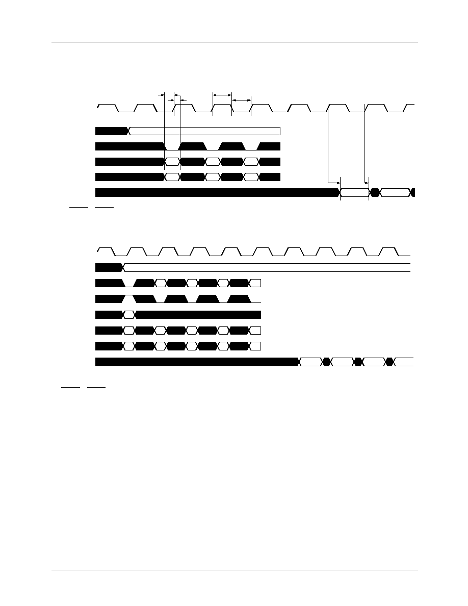
Timing Diagrams
No Accumulation
Note: OERX = OEPY = LOW
Phase Modulation
Notes:
1. OERX = OEPY = LOW
2. Carrier C and amplitude R loaded on CLK0.
3. Modulation Values I, J, K, L... Loaded on CLK1, CLK2, etc.
4. Output corresponding to modulation loaded at CLKi emerged tDO after CLKi + 21.
5. To modulate amplitude, vary XRIN with ENXR = 1.
CLK
00
0
1
2
3
...
...
...
...
...
...
22
f(A)
f(B)
23
tH
tD
tHO
tS
tPWH
tPWL
RTP, TCXY
ACC[1:0]
ENXR,
ENYP[1:0]
XRIN[15:0],
YPIN[31:0]
RXOUT[15:0],
PYOUT[15:0]
00
00
EN
EN
EN
A
B
C
CLK
00
01
01
01
01
0
1
2
3
...
22
23
24
25
...
...
...
...
...
RTP, TCXY
ACC[1:0]
ENXR
ENYP[1:0]
XRIN[15:0]
YPIN[31:0]
RXOUT[15:0]
PYOUT[15:0]
R
10
01
01
01
01
C
I
J
K
L
C + I
2C + J
3C + K
4C + L
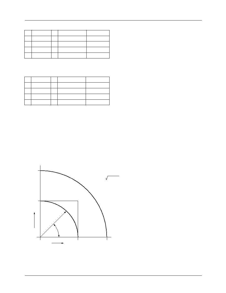
Applications Discussion
Numeric Overflow
Because the TMC2330A accommodates 16-bit unsigned
radii and 16-bit signed Cartesian coordinates, Polar-To-
Rectangular conversions can overflow for incoming radii
greater than 32767= 7FFFh and will overflow for all incom-
ing radii greater than 46341=B505h. (ln signed magnitude
mode, a radius of 46340 = B504h will also overflow at all
angles.) The regions of overflow and of correct conversion
are illustrated in Figure 1.
In signed magnitude mode, overflows are circularly symmet-
rical--if a given radius overflows at an angle P, it will also
overflow at the angles
-P, +P, and -P. This is because -X
will overflow if and only if X overflows, and -Y will over-
flow if and only if Y overflows.
In two's complement mode, the number system's asymmetry
complicates the overflow conditions slightly. An input vector
with an X component of -32768=8000h will not overflow,
whereas one with an X component of +32768 will. Table 3
summarizes several simple cases of overflow and near-over-
flow.
TMC2330A
PRODUCT SPECIFICATION
REV. 1.1.8 10/31/00
11
Table 3a. X-Dimensional Marginal Overflows
In all cases, RTP=0 (Polar-To-Rectangular mode) and
XRIN=8000 (incoming radius=32768).
Table 3b. Maximal Overflow (Radius In=65535)
In all cases, RTP=0 (Polar-To-Rectangular mode) and
XRIN=7FFF (incoming radius=65535, which will always
overflow).
Numeric Underflow
In RTP=1 (Rectangular-To-Polar) mode, if XRIN=YPIN=0, the
angle is undefined. Under these conditions, the TMC2330A
will output the expected radius of 0 (RXOUT= 0000) and an
angle of 1.744 radians (PYOUT=4707). This angle is an artifact
of the CORDIC algorithm and is not flagged as an error,
since the angle of any 0 length vector is arbitrary.
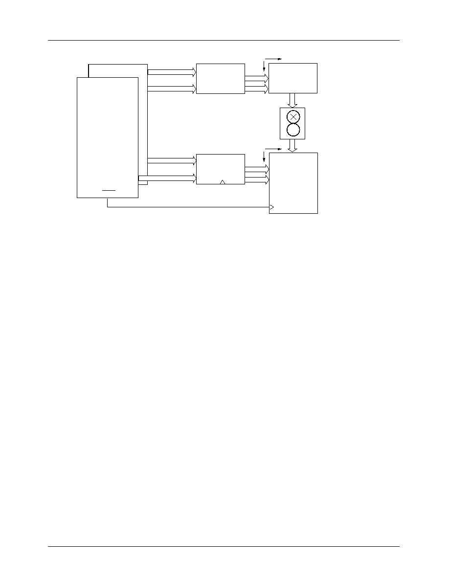
Performing Scan Conversion with
the TMC2330A
Medical Imaging Systems such as Ultrasound, MRI, and
PET, and phased array Radar and Sonar systems generate
radial-format coordinates (range or distance, and bearing)
which must be converted into raster-scan format for further
processing and display. Utilizing the TMC2302A Image
Resampling Sequencer, a minimum chipcount Scan Con-
verter can be implemented which utilizes the trigonometric
translation performed by the TMC2330A to backwards-map
from a Cartesian coordinate set into the Polar source image
buffer address space.
As shown in Figure 2, the TMC2330A transforms the Carte-
sian source image addresses from the TMC2302A directly to
vector distance and angle coordinates, while the TMC2302A
writes the resulting resampled pixel values into the target
memory in raster fashion. Note that the ability to perform
this spatial transformation in either direction gives the user
the freedom to process images in either coordinate space,
with little restriction. Image manipulation such as zooms or
tilts can easily be included in the transformation by program-
ming the desired image manipulation into the TMC2302A's
transformation parameter registers.
TC YPIN
OV RXOUT
CORRECT
X
0
0000 = 0
1
0000 = +0
+32768
0
8000 =
1
8000 = -0
-32768
1
0000 = 0
1
8000 = -32768
+32768
1
8000 =
0
8000 = -32768
-32768
TC YPIN
OV RXOUT
CORRECT
X
0
0000 = 0
1
7FFF = +32767
+65535
0
8000 =
1
FFFF = -32767
-65535
1
0000 = 0
1
FFFF = -1
+65535
1
8000 =
1
0001 = +1
-65535
Figure 1. First Quadrant Coordinate Relationships
65535
32767
C
B
A
R
X
32767
65535
Y
/2
X = R (Cos
)
Y = R (Sin
)
and
R = X2 + Y2
= Tan-1 (Y/X)
If R
32767, overflow will not occur (Region A).
If R > 32767, overflow will not occur (Region B) if |X|
32767 and |Y| 32767.
If R > 32767, overflow will occur (Region C) if |X|
32768 or |Y| 32768.
PRODUCT SPECIFICATION
TMC2330A
12
REV. 1.1.8 10/31/00
Arithmetic Error for Two's
Complement Rectangular to Polar
Conversion
A random set of 5000 input vector coordinate pairs (X,Y),
uniformly spread over a circle of radius 32767 was converted
to polar coordinates.
Radius Error Range
0.609 to 0.746 LSB
Mean Radius Error
0.019 LSB
Mean Absolute Radius Error
0.252 LSB
Phase Error Range
1.373 to 1.469 LSB
Mean Phase Error
0.058 LSB
Mean Absolute Phase Error
0.428 LSB
Statistical Evaluation of Double
Conversion
In this empirical test, 10,000 random Cartesian vectors were
converted to and from polar format by the TMC2330A. The
resulting Cartesian pairs were then compared against the
original ones. The un-restricted database represents uniform
sampling over a square bounded by -32769<x<32768 and
-32769<y<32768.
The results of the 10,000-vector study were as follows:
Mean Error (X)
+0.0052 LSB
Mean Error (Y)
0.0031 LSB
Mean Absolute Error (X)
0.662 LSB
Mean Absolute Error (Y)
0.664 LSB
Root Mean Square Error (X)
1.025 LSB
Root Mean Square Error (Y)
1.020 LSB
Max Error (X)
+4/ -5 LSB
Max Error (Y)
+5 -4 LSB
Since this is a double conversion (rectangular to polar and
back) which includes a wide variety of "good case" and "bad
case" vectors, the chip should perform even better in many
real systems. Repeating the experiment and restricting the
original data set to an annulus defined by 8196<R<32768
reduced the mean square error to 0.89 LSB and the peak
error to ±4 LSB (x or y). These latter results are more ger-
mane to synthesizer, demodulator, and other applications in
which the amplitude can be restricted to lie between quarter
and full scale. The largest errors tend to occur in the angle
component of small radius cartesian-to-polar conversion.
Figure 1. Figure 1. First Quadrant Coordinate Relationships
Figure 2. Block Diagram of Scan Converter Circuit Utilizing TMC2330A and TMC2302A Image Resampling Sequencer
SADR
SADR
X
Y
R
R
SOURCE
IMAGE BUFFER
DATA OUT
(4) TMC2011A
DELAY
REGISTER
DATA IN
TARGET
IMAGE
BUFFER
TADR
TADR
U
V
TWR
U
V
TMC2246A
PIXEL INTERPOLATOR
(2) TMC2302A IMAGE
RESAMPLING
SEQUENCERS
TMC2330A
COORDINATE
TRANSFORMER
TMC2330A
PRODUCT SPECIFICATION
REV. 1.1.8 10/31/00
13
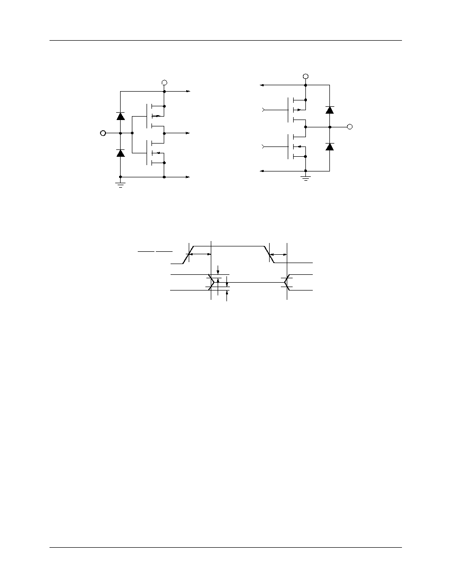
Equivalent Circuits
Figure 3. Equivalent Input Circuit
Figure 4. Equivalent Output Circuit
Digital
Input
V
DD
p
n
GND
V
DD
p
n
GND
Digital
Output
Figure 5. Transition Levels for Three-State Measurements
2.0V
0.8V
t
DIS
t
ENA
Three-State
Outputs
OERX, OEPY
High Impedance
0.5V
0.5V
PRODUCT SPECIFICATION
TMC2330A
14
REV. 1.1.8 10/31/00
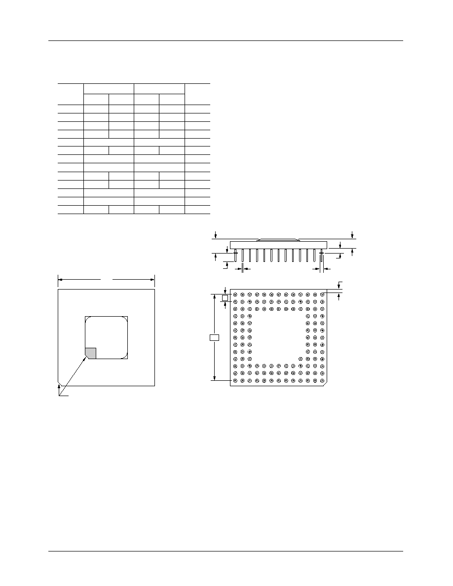
Mechanical Dimensions
120-Lead CPGA Package
D
Pin 1 Identifier
Top View
Cavity Up
D1
P
L
A2
A
øB
e
øB2
A1
A
.080
.160
2.03
4.06
Symbol
Inches
Min.
Max.
Min.
Max.
Millimeters
Notes
A1
.040
.060
1.01
1.53
.215
5.46
A2
.125
3.17
øB
.016
.020
0.40
0.51
D
1.340
1.380
33.27
35.05
2
2
SQ
D1
.110
.145
2.79
3.68
e
.050 NOM.
1.27 NOM.
1.200 BSC
30.48 BSC
.100 BSC
2.54 BSC
L
L1
.170
.190
4.31
4.83
.003
--
.076
--
M
13
13
120
120
3
4
N
P
øB2
Notes:
1.
2.
3.
4.
5.
6.
Pin #1 identifier shall be within shaded area shown.
Pin diameter excludes solder dip finish.
Dimension "M" defines matrix size.
Dimension "N" defines the maximum possible number of pins.
Orientation pin is at supplier's option.
Controlling dimension: inch.
PRODUCT SPECIFICATION
TMC2330A
15
REV. 1.1.8 10/31/00
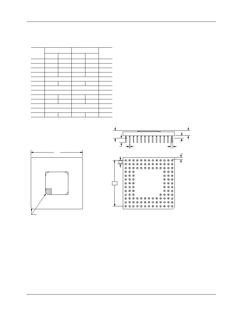
Mechanical Dimensions
120-Lead PPGA Package
D
Pin 1 Identifier
Top View
Cavity Up
D1
P
L
A2
A
øB
e
øB2
A1
A
.080
.160
2.03
4.06
Symbol
Inches
Min.
Max.
Min.
Max.
Millimeters
Notes
A1
.040
.060
1.01
1.53
.215
5.46
A2
.125
3.17
øB
.016
.020
0.40
0.51
D
1.340
1.380
33.27
35.05
2
2
SQ
D1
.110
.145
2.79
3.68
e
.050 NOM.
1.27 NOM.
1.200 BSC
30.48 BSC
.100 BSC
2.54 BSC
L
L1
.170
.190
4.31
4.83
.003
--
.076
--
M
13
13
120
120
3
4
N
P
øB2
Notes:
1.
2.
3.
4.
5.
6.
Pin #1 identifier shall be within shaded area shown.
Pin diameter excludes solder dip finish.
Dimension "M" defines matrix size.
Dimension "N" defines the maximum possible number of pins.
Orientation pin is at supplier's option.
Controlling dimension: inch.
PRODUCT SPECIFICATION
TMC2330A
16
REV. 1.1.8 10/31/00
Mechanical Dimensions
120-Lead Metric Quad Flat Package to Pin Grid Array Package (MPGA)
D
Pin 1 Identifier
Fairchild
TMC2330A
D1
A
A2
L
e
øB
øB2
A1
A3
e
A
.309
.311
7.85
7.90
Symbol
Inches
Min.
Max.
Min.
Max.
Millimeters
Notes
A1
.145
.155
3.68
3.94
.090
2.29
A2
A3
.080
2.03
øB
.016
.020
0.40
0.51
D
1.355
1.365
34.42
34.67
2
2
SQ
D1
.175
.185
4.45
4.70
e
.050 NOM.
1.27 NOM.
.050 TYP.
1.27 TYP.
1.200 BSC
30.48 BSC
.100 BSC
2.54 BSC
L
M
13
13
120
120
3
4
N
øB2
Notes:
1.
2.
3.
4.
5.
6.
Pin #1 identifier shall be within shaded area shown.
Pin diameter excludes solder dip finish.
Dimension "M" defines matrix size.
Dimension "N" defines the maximum possible number of pins.
Orientation pin is at supplier's option.
Controlling dimension: inch.
TMC2330A
PRODUCT SPECIFICATION
REV. 1.1.8 10/31/00
17
Mechanical Dimensions
120-Pin MQFP Package
D
D1
E1
E
e
PIN 1 IDENTIFIER
A2
A1
A
B
Base Plane
Seating Plane
See Lead Detail
C
0
° Min.
R
0.063" Ref (1.60mm)
Lead Detail
L
.20 (.008) Min.
.13 (.005) R Min.
-C-
ccc C
LEAD COPLANARITY
Notes:
1.
2.
3.
4.
5.
All dimensions and tolerances conform to ANSI Y14.5M-1982.
Controlling dimension is millimeters.
Dimension "B" does not include dambar protrusion. Allowable
dambar protrusion shall be .08mm (.003in.) maximum in excess
of the "B" dimension. Dambar cannot be located on the lower
radius or the foot.
"L" is the length of terminal for soldering to a substrate.
"B" & "C" includes lead finish thickness.
A
--
.154
--
3.92
Symbol
Inches
Min.
Max.
Min.
Max.
Millimeters
Notes
A1
.010
--
.25
--
.018
.45
A2
.125
.144
3.17
3.67
B
.012
3, 5
.30
.009
.23
C
.005
.13
D1/E1
1.098
1.106
27.90
28.10
.0315 BSC
.80 BSC
e
L
.026
.037
.65
.95
120
120
30
30
4
5
N
ND
0
°
7
°
0
°
7
°
--
.004
--
.10
ccc
D/E
1.219
1.238
30.95
31.45
.13/.30
.005/.012
PRODUCT SPECIFICATION
TMC2330A
LIFE SUPPORT POLICY
FAIRCHILD'S PRODUCTS ARE NOT AUTHORIZED FOR USE AS CRITICAL COMPONENTS IN LIFE SUPPORT DEVICES
OR SYSTEMS WITHOUT THE EXPRESS WRITTEN APPROVAL OF THE PRESIDENT OF FAIRCHILD SEMICONDUCTOR
CORPORATION. As used herein:
1. Life support devices or systems are devices or systems
which, (a) are intended for surgical implant into the body, or
(b) support or sustain life, and (c) whose failure to perform
when properly used in accordance with instructions for use
provided in the labeling, can be reasonably expected to
result in a significant injury of the user.
2. A critical component in any component of a life support
device or system whose failure to perform can be
reasonably expected to cause the failure of the life support
device or system, or to affect its safety or effectiveness.
www.fairchildsemi.com
10/31/00 0.0m 002
Stock#DS30002230A
2000 Fairchild Semiconductor Corporation
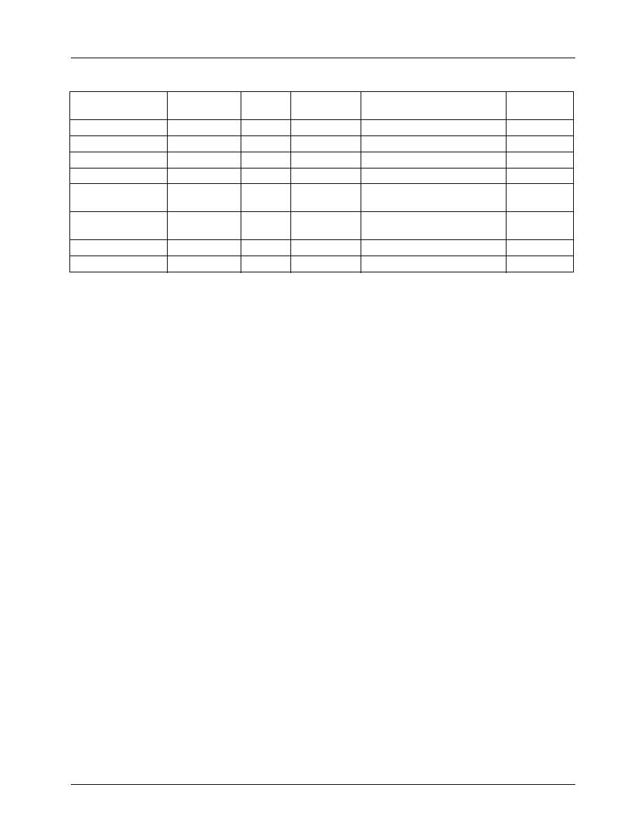
Ordering Information
Product Number
Temperature
Range
Speed
Grade
Screening
Package
Package
Marking
TMC2330AG1C
0° to 70°C
20 MHz
Commercial
120-Pin Ceramic Pin Grid Array
2330AG1C
TMC2330AG1C1
0° to 70°C
40 MHz
Commercial
120-Pin Ceramic Pin Grid Array 2330AG1C1
TMC2330AH5C
0° to 70°C
20 MHz
Commercial
120-Pin Plastic Pin Grid Array
2330AH5C
TMC2330AH5C1
0° to 70°C
40 MHz
Commercial
120-Pin Plastic Pin Grid Array
2330AH5C1
TMC2330AH6C
0° to 70°C
20 MHz
Commercial
120 Lead Metric Quad FlatPack
to Pin Grid Array
N/A
TMC2330AH6C1
0° to 70°C
40 MHz
Commercial
120 Lead Metric Quad FlatPack
to Pin Grid Array
N/A
TMC2330AKEC
0° to 70°C
20 MHz
Commercial
120-Pin Metric Quad FlatPack
2330AKEC
TMC2330AKEC1
0° to 70°C
40 MHz
Commercial
120-Pin Metric Quad FlatPack
2330AKEC1