 | ÐлекÑÑоннÑй компоненÑ: TMC2490A | СкаÑаÑÑ:  PDF PDF  ZIP ZIP |
Äîêóìåíòàöèÿ è îïèñàíèÿ www.docs.chipfind.ru
www.fairchildsemi.com
REV. 1.0.2 2/27/02
Features
· All-digital video encoding
· Internal digital subcarrier synthesizer
· 8-bit parallel CCIR-601/CCIR-656/ANSI/SMPTE
125M input format
· CCIR-624/SMPTE-170M compliant output
· Switchable chrominance bandwidth
· Switchable pedestal with gain compensation
· Pre-programmed horizontal and vertical timing
· 13.5 Mpps pixel rate
· Master or slave (CCIR656) operation
· MPEG interface
· Internal interpolation filters simplify output
reconstruction filters
· 10-bit D/A converters for video reconstruction
· Supports NTSC and PAL standards
· Closed-caption waveform insertion
· Simultaneous S-Video (Y/C) output
· Controlled edge rates
· Single +5V power supply
· 44 lead PLCC package
· Parallel and serial control interface
Applications
· Set-top digital cable television receivers
· Set-top digital satellite television receivers
· Studio parallel CCIR-601 to analog conversion
Description
The TMC2490A video encoder converts digital component
video (in 8-bit parallel CCIR-601/656 or ANSI/SMPTE
125M format) into a standard analog baseband television
(NTSC, NTSC-EIA, and all PAL standards) signal with a
modulated color subcarrier. Both composite (single lead) and
S-Video (separate chroma and luma) formats are active
simultaneously at all three analog outputs. Each video output
generates a standard video signal capable of driving a singly-
or doubly-terminated 75 Ohm load.
The TMC2490A is intended for all non-Macrovision
encoder applications.
The TMC2490A is fabricated in a submicron CMOS
process and is packaged in a 44-lead PLCC. Performance is
guaranteed over the full 0
°
C to 70
°
C operating temperature
range.
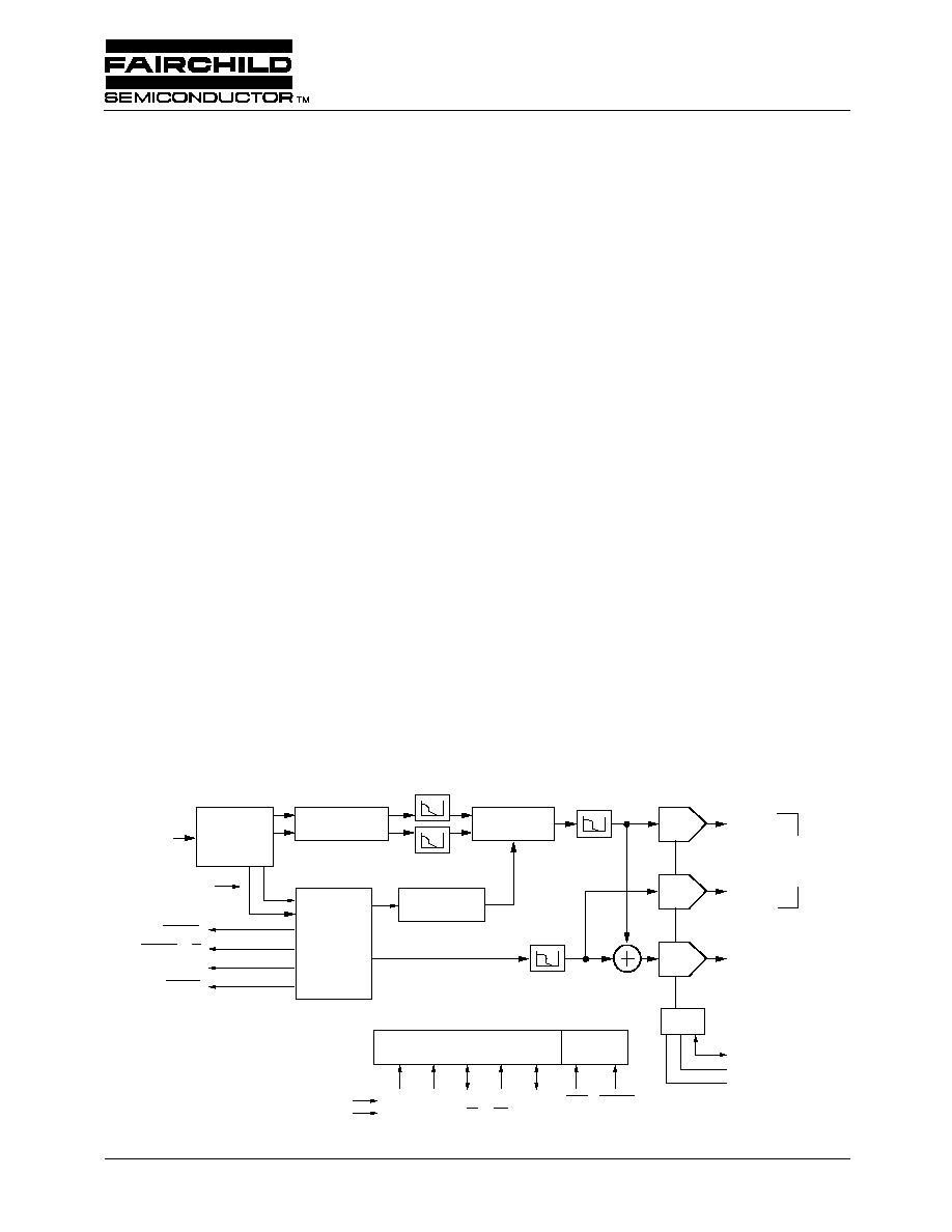
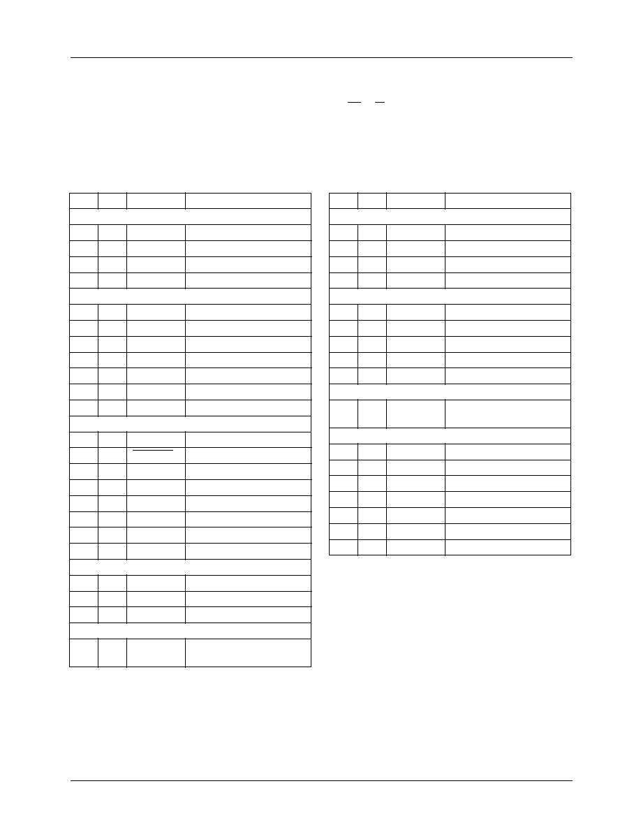
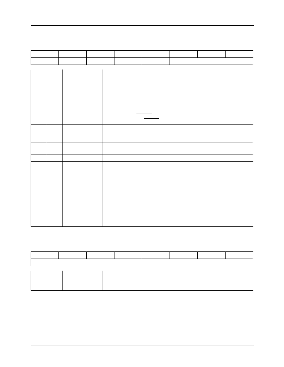
Block Diagram
PIXEL DATA
DEMUX AND
SYNC
EXTRACT
DIGITAL
SYNC AND
BLANK
GENERATOR
PD
7-0
HSYNC
VSYNC, B/T
SELC
PXCK
Y
PDC/CBSEL
INTERPOLATOR
4:2:2 TO 4:4:4
CHROMA
MODULATOR
GLOBAL
CONTROL
SERIAL/PARALLEL CONTROL
SUBCARRIER
SYNTHESIZER
CHROMA
10-BIT
D/A
INTER-
POLATION
FILTER
B-Y
LPF
LPF
R-Y
LUMA
10-BIT
D/A
COMPOSITE
V
REF
C
BYP
R
REF
10-BIT
D/A
REF
RESET
65-2490(1)A-01
SER
INTER-
POLATION
FILTER
D
7-0
D
7-0
SCL
CS
SDA
R/W
SA
0
ADR
SA
1
SERIAL
PARALLEL
S-VIDEO
TMC2490A
Multistandard Digital Video Encoder
TMC2490A
PRODUCT SPECIFICATION
2
REV. 1.0.2 2/27/02
Functional Description
The TMC2490A is a fully-integrated digital video encoder
with simultaneous composite and Y/C (S-Video) outputs,
compatible with NTSC, NTSC-EIA, and all PAL television
standards.
Digital component video is accepted at the PD port in 8-bit
parallel CCIR-601/656 format. It is demultiplexed into
luminance and chrominance components. The chrominance
components modulate a digitally synthesized subcarrier.
The luminance and chrominance signals are then separately
interpolated to twice the input pixel rate and converted to
analog signals by 10-bit D/A converters. They are also
digitally combined and the resulting composite signal is
output by a third 10-bit D/A converter.
The TMC2490A operates from a single clock at 27 MHz,
twice the system pixel rate. Programmable control registers
allow software control of subcarrier frequency and phase
parameters. Incoming YC
B
C
R
422 digital video is interpo-
lated to YC
B
C
R
444 format for encoding.
Internal control registers can be accessed over a standard
8-bit parallel microprocessor port or a 2-pin (clock and data)
serial port.
Sync Generator
The TMC2490A operates in master or slave mode. In slave
mode, it extracts its horizontal and vertical sync timing and
field information from the CCIR-656 SAV (Start of Active
Video) and EAV (End of Active Video) signal in the incom-
ing data stream. In master mode, it generates a 13.5 MHz
timebase and sends line and field synchronizing signals to
the host system.
Horizontal and vertical synchronization pulses in the analog
output are digitally generated by the TMC2490A with con-
trolled rise and fall times on all sync edges, the beginning
and end of active video, and the burst envelope.
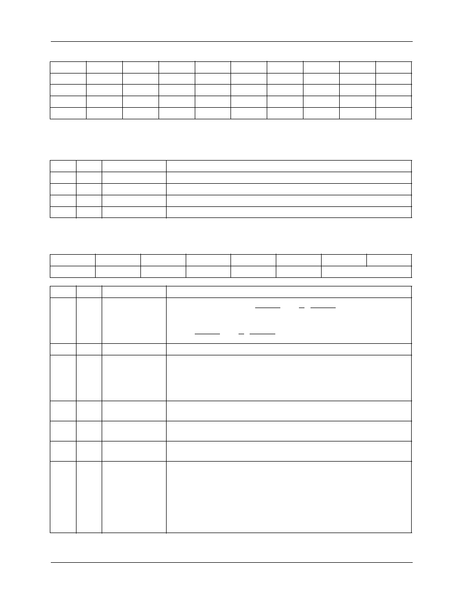
Figure 1. Pixel Data Format
Chroma Modulator
A digital subcarrier synthesizer generates the reference for
a quadrature modulator, producing a digital chrominance
signal. The chroma bandwidth may be programmed to
650 kHz or 1.3 MHz.
Interpolation Filters
Interpolation filters on the luminance and chrominance
signals double the pixel rate to 27Mpps before D/A conver-
sion. This low-pass filtering and oversampling process
reduces sin(x)/x roll-off, and greatly simplifies the analog
reconstruction filter required after the D/A converters.
D/A Converters
Analog outputs of the TMC2490A are driven by three 10-bit
D/A converters, The outputs drive standard video levels into
37.5 or 75 Ohm loads. An internal voltage reference is used
to provide reference current for the D/A converters. An
external fixed or variable voltage reference source can also
be used. The video signal levels from the TMC2490A may
be adjusted to overcome the insertion loss of analog low-pass
output filters by varying R
REF
or V
REF
.
Parallel and Serial Microprocessor Interfaces
The parallel microprocessor interface employs 11 pins.
These are shared with the serial interface. A single pin, SER,
selects between the two interface modes.
In parallel interface mode, one address pin is decoded to
enable access to the internal control register and its pointer.
Controls are reached by loading a desired address through
the 8-bit D
7-0
port, followed by the desired data (read or
write) for that address. The control register address pointer
auto-increments to address 22h and then remains there.
A 2-line serial interface is also provided on the TMC2490A
for initialization and control. The same set of registers
accessed by the parallel port is available to the serial port.
The RESET pin sets all internal state machines and control
registers to their initialized conditions, disables the analog
outputs, and places the encoder in a reset mode. At the rising
edge of RESET, the encoder is automatically initialized in
NTSC-M format.
MSB
LSB
PD
7
C
B
(n)
PD
0
PD
7
Y (n)
PD
0
PD
7
C
R
(n)
PD
0
PD
7
Y (n+1)
PD
0
PRODUCT SPECIFICATION
TMC2490A
3
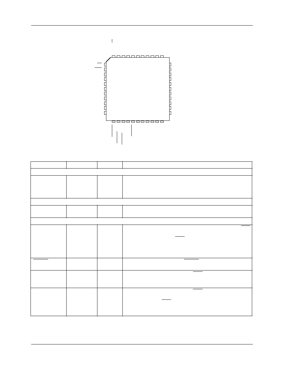
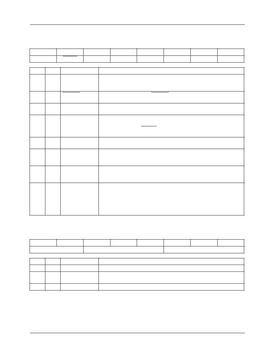
Pin Assignments
Pin Descriptions
Pin Name
Pin Number
Value
Pin Function Description
Clock
PXCK
25
TTL
Pixel Clock Input.
This 27.0 MHz clock is internally divided by 2
to generate the internal pixel clock. PXCK drives the entire
TMC2490A, except the asynchronous microprocessor interface.
All internal registers are strobed on the rising edge of PXCK.
Data Input Port
PD
7-0
3844, 3
TTL
Pixel Data Inputs.
Video data enters the TMC2490A on
PD
7-0
(Figure 1).
Microprocessor Interface
D
7-0
912, 1417
TTL
Data I/O, General Purpose I/O, Chroma Input Port.
When SER
is HIGH, all control parameters are loaded into and read back
over this 8-bit port. When SER = LOW, D
0
can serve as a
composite sync output, D
1
outputs a burst flag during the back
porch, D
2-5
are General Purpose Outputs, and D
6-7
are General
Purpose Inputs.
RESET
22
TTL
Master Reset Input.
Bringing RESET LOW forces the internal
state machines to their starting states and disables all outputs.
SA
1
4
TTL
Serial/Parallel Port Select.
When SER is LOW, SA
1
in
conjunction with SA
0
selects one of four addresses for the
TMC2490A.
SA
0
, ADR
5
TTL
Serial/Parallel Port Select.
When SER is LOW, SA
0
in
conjunction with SA
1
selects one-of-four addresses for the
TMC2490A. When SER is HIGH, this control governs whether the
parallel microprocessor interface selects a table address or
reads/writes table contents.
65-2490(1)A-02
SCL/CS
SER
D
7
D
6
D
5
D
4
GND
D
3
D
2
D
1
D
0
PD
6
PD
7
V
DD
GND
CHROMA
V
DDA
C
BYP
LUMA
GND
COMPOSITE
GND
SDA/R/W
SA
0
/ADR
SA
1
PD
0
GND
V
DD
PD
1
PD
2
PD
3
PD
4
PD
5
HSYNC
VSYNC,T/B
CBSEL,PDC
SELC
RESET
V
DD
GND
PXCK
V
DD
V
REF
R
REF
7
8
9
10
11
12
13
14
15
16
17
39
38
37
36
35
34
33
32
31
30
29
18
19
20
21
22
23
24
25
26
27
28
6
5
4
3
2
1
44
43
42
41
40
TMC2490A
TMC2490A
PRODUCT SPECIFICATION
REV. 1.0.2 2/27/02
4
SDA, R/W
6
R-Bus/TTL
Serial Data/Read/Write Control.
When SER is LOW, SDA is the
data line of the serial interface. When SER is HIGH, the pin is the
read/write control for the parallel interface. When R/W and CS are
LOW, the microprocessor can write to the control registers over
D
7-0
. When R/W is HIGH and CS is LOW, it can read the
contents of any selected control register over D
7-0
.
SCL, CS
7
R-Bus/TTL
Serial Clock/Chip Select.
When SER is LOW, SCL is the clock
line of the serial interface. When SER is HIGH, the pin is the chip
select control for the parallel interface. When CS is HIGH, the
microprocessor interface port, D
7-0
, is set to HIGH impedance
and ignored. When CS is LOW, the microprocessor can read or
write parameters over D
7-0
.
SER
8
TTL
Serial/Parallel Port Select.
When LOW, the 2-line serial
interface is activated. Pins 5, 6, and 7 function as SA
0
, SDA, and
SCL respectively. When HIGH, the parallel interface port is active
and pins 5, 6, and 7 function as ADR, R/W, and CS respectively.
Outputs
CHROMA
35
1.35V p-p
Chrominance-only Video.
Analog output of chrominance D/A
converter. Maximum output is 1.35 volts peak-to-peak into a
doubly terminated 75 Ohm load.
COMPOSITE
30
1.35V p-p
Composite NTSC/PAL Video.
Analog output of composite D/A
converter. Maximum output is 1.35 volts peak-to-peak into a
doubly terminated 75 Ohm load.
LUMA
32
1.35V p-p
Luminance-only Video.
Analog output of luminance D/A
converter. Maximum output is 1.35 volts peak-to-peak into a
doubly terminated 75 Ohm load.
Analog Interface
C
BYP
33
0.1
µ
F
Reference Bypass Capacitor.
Connection point for 0.1
µ
F
decoupling capacitor to V
DD
at pin 34.
R
REF
28
787
Current-setting Resistor.
Connection point for external current-
setting resistor for D/A converters. The resistor is connected
between R
REF
and GND. Output video levels are inversely
proportional to the value of R
REF
.
V
REF
27
+1.235V
Voltage Reference Input.
External voltage reference input,
internal voltage reference output, nominally 1.235 V.
SYNC Out
HSYNC
18
TTL
Horizontal Sync Output.
VSYNC, T/B
19
TTL
Vertical Sync Output or Odd/Even Field ID Output
.
CBSEL, PDC
20
TTL
Pixel Data Phase Output or Video Blanking Output.
SELC
21
TTL
Luma/Chroma MUX Control.
Power Supply
V
DD
1, 23, 26, 37
+5V
Power Supply.
Positive power supply.
GND
2, 13, 24, 29,
31, 36
0.0V
Ground.
V
DDA
34
+5V
Analog Power Supply.
Positive power supply.
Pin Descriptions
(continued)
Pin Name
Pin Number
Value
Pin Function Description
PRODUCT SPECIFICATION
TMC2490A
REV. 1.0.2 2/27/02
5
Control Registers
The TMC2490A is initialized and controlled by a set of reg-
isters which determine the operating modes.
An external controller is employed to write and read the
Control Registers through either the 8-bit parallel or 2-line
serial interface port. The parallel port, D
7-0
, is governed by
pins CS, R/W, and ADR. The serial port is controlled by
SDA and SCL.
Table 1. Control Register Map
Reg
Bit
Mnemonic
Function
TMC2490A Identification Registers (Read only)
00
7-0
PARTID2
Reads back 97h
01
7-0
PARTID1
Reads back 24h
02
7-0
PARTID0
Reads back 90h (91h)
03
7-0
REVID
Silicon revision #
Global Control Register
04
7
MASTER
Master Mode
04
6
NGSEL
NTSC Gain Select
04
5
YCDELAY
Luma to chroma delay
04
4
RAMPEN
Modulated ramp enable
04
3
YCDIS
LUMA, CHROMA disable
04
2
COMPDIS
COMPOSITE disable
04
1-0
FORMAT
Television standard select
Video Output Control Register
05
7
PALN
Select PAL-N Subcarrier
05
6
BURSTF
Burst flag disable
05
5
CHRBW
Chroma bandwidth select
05
4
SYNCDIS
Sync pulse disable
05
3
BURDIS
Color burst disable
05
2
LUMDIS
Luminance disable
05
1
CHRDIS
Chrominance disable
05
0
PEDEN
Pedestal enable
Field ID Register
06
7-6
Reserved
Program LOW
06
5-3
FIELD
Field ID (Read only)
06
2-0
Reserved
Program LOW
Reserved Registers
07-
0D
7-0
Reserved
Program LOW
Notes:
1. For each register listed above, all bits not specified are
reserved and should be set to logic LOW to ensure proper
operation.
General Purpose Port Register
0E
7
PORT7-6
General purpose Inputs
0E
6
PORT5-2
General purpose Outputs
0E
1
BURSTF
Burst Flag Output
0E
0
CSYNC
Composite Sync Output
General Control Register
0F
7
PED21
VBI Pedestal Enable
0F
5
VSEL
Vertical Sync Select
0F
4
CBSEL
CBSEL/PDC Pin Function
0F
3
VBIEN
VBI Pixel Data Enable
0F
1-0
HDSEL
HSYNC Delay
Reserved Registers
10-
1F
7-0
Reserved
May be left unprogrammed
Closed-Caption Insertion Registers
20
7-0
CCD1
First Byte of CC Data
21
7-0
CCD2
Second Byte of CC Data
22
7
CCON
Enable CC Data Packet
22
6
CCRTS
Request To Send Data
22
5
CCPAR
Auto Parity Generation
22
4
CCFLD
CC Field Select
22
3-0
CCLINE
CC Line Select
Reg
Bit
Mnemonic
Function
TMC2490A
PRODUCT SPECIFICATION
REV. 1.0.2 2/27/02
6
Table 2. Default Register Values on Reset
Control Register Definitions
Reg
Dflt
Reg
Dflt
Reg
Dflt
Reg
Dflt
Reg
Dflt
00
97
04
00
08
00
0C
00
20
80
01
24
05
01
09
00
0D
00
21
80
02
90(91)
06
00
0A
00
0E
00
22
00
03
xx
07
00
0B
00
0F
F2
Reg
Bit
Name
Description
00
70
PARTID2
Reads back 97h
01
70
PARTID1
Reads back 24h
02
70
PARTID0
Reads back 90h (91h)
03
70
REVID
Reads back a value corresponding to the revision letter of the silicon.
Global Control Register (04)
7
6
5
4
3
2
1
0
MASTER
NGSEL
YCDELAY
RAMPEN
YCDIS
COMPDIS
FORMAT
Reg
Bit
Name
Description
04
7
MASTER
Master Mode. When MASTER = 1, the encoder generates its own video
timing and outputs signals VSYNC (or T/B), HSYNC, SELC, and PDC (or
CBSEL). When MASTER = 0, the TMC2490A extracts timing from the
embedded EAV codeword in the video datastream and optionally outputs
signals VSYNC (or T/B), HSYNC, SELC, and PDC (or CBSEL).
04
6
NGSEL
NTSC Gain Selection.
04
5
YCDELAY
Luma to chroma delay. When HIGH, the luminance path within the
TMC2490A is delayed by one PXCK period. The delay applies to both
COMPOSITE and LUMA outputs and may be used to compensate for group
delay variation of external filters. When LOW, luminance and chrominance
have the same latency.
04
4
RAMPEN
Modulated ramp enable. When HIGH, the TMC2490A outputs a modulated
ramp test signal. When LOW, incoming digital video is encoded.
04
3
YCDIS
LUMA, CHROMA disable. When HIGH, the LUMA and CHROMA outputs
are disabled. Set LOW for normal enabled operation.
04
2
COMPDIS
COMPOSITE disable. When HIGH, the COMPOSITE output is disabled.
Set LOW for normal enabled operation.
04
10
FORMAT
Television standard select. Selects basic H&V timing parameters and
subcarrier frequency. Pedestal level and chrominance bandwidth are
independently programmed.
0 0 NTSC
0 1 PAL-B,G,H,I,N
1 0 PAL-M
1 1 Reserved
PRODUCT SPECIFICATION
TMC2490A
7
Control Register Definitions
(continued)
Video Output Control Register (05)
7
6
5
4
3
2
1
0
PALN
BURSTF
CHRBW
SYNCDIS
BURDIS
LUMDIS
CHRDIS
PEDEN
Reg
Bit
Name
Description
05
7
PALN
Select PAL-N Subcarrier. When HIGH, selects PAL-N subcarrier
frequency. When LOW, the encoder produces the PAL-B,G,H,I subcarrier.
Program LOW for NTSC and PAL-M video.
05
6
BURSTF
Burst flag disable. When BURSTF is LOW, a clamp gate signal is
produced on the D1 output and register 0E bit 1.
05
5
CHRBW
Chroma bandwidth select. When LOW, the chrominance bandwidth is
±650 kHz. When HIGH, the chrominance bandwidth is ±1.3 MHz.
05
4
SYNCDIS
Sync pulse disable. When HIGH, horizontal and vertical sync pulses on the
COMPOSITE video output are suppressed (to blanking level). Color burst,
active video, and the CSYNC output remain active. Set LOW for normal
composite video operation.
05
3
BURDIS
Color burst disable. When HIGH, color burst is suppressed to the blanking
level. Set LOW for normal operation.
05
2
LUMDIS
Luminance disable. When HIGH, incoming Y values are forced to black
level. Color burst, CHROMA, and sync are not affected. Set LOW for normal
operation.
05
1
CHRDIS
Chrominance disable. When HIGH, incoming color components C
B
and
C
R
are suppressed, enabling monochrome operation. Output color burst is
not affected. Set LOW for normal color operation.
05
0
PEDEN
Pedestal enable. When LOW, black and blanking are the same level for
ALL lines. When HIGH, a 7.5 IRE pedestal is inserted into the output video
for NTSC and PAL-M lines 23-262 and 286-525 only. Chrominance and
luminance gain factors are adjusted to keep video levels within range.
PEDEN is valid for NTSC and PAL-M only and should be LOW for all other
formats.
Field Data Register (06)
7
6
5
4
3
2
1
0
Reserved
FIELD
Reserved
Reg
Bit
Name
Description
06
76
Reserved
Program LOW.
06
53
FIELD
Field ID (Read only). A value of 000 corresponds to field 1 and 111
corresponds to field 8.
06
20
Reserved
Program LOW.
TMC2490A
PRODUCT SPECIFICATION
REV. 1.0.2 2/27/02
8
Control Register Definitions
(continued)
Reserved Registers (070D)
7
6
5
4
3
2
1
0
Reserved
Reg
Bit
Name
Description
07
0D
70
Reserved
Program LOW.
General Purpose Port Register (0E)
7
6
5
4
3
2
1
0
PORT7
PORT6
PORT5
PORT4
PORT3
PORT2
BURSTF
CSYNC
Reg
Bit
Name
Description
0E
76
PORT76
General purpose Inputs. When in serial control mode, these register read-
only bits indicate the state present on data port pins D
7
and D
6
.
0E
52
PORT52
General purpose Outputs. When in serial control mode or when reading
register 0E in parallel control mode, these register read/write bits drive data
pins D
5
D
2
to the state contained in the respective register bits.
0E
1
BURSTF
Burst Flag Output. Produces Burst Flag on data pin D
1
when in serial
control mode, or when reading register 0E.
0E
0
CSYNC
Composite Sync Output. Produces Composite Sync on data pin D
0
when
in serial control mode, or when reading register 0E.
PRODUCT SPECIFICATION
TMC2490A
9
Control Register Definitions
(continued)
General Control Register (0F)
7
6
5
4
3
2
1
0
PED21
Reserved
VSEL
CBSEL
VBIEN
Reserved
Reg
Bit
Name
Description
0F
7
PED21
VBI Pedestal Enable. When HIGH and FORMAT is 00 (NTSC) or 10
(PAL-M), pedestal is added to lines 21, 22, 283, 284, 285. When LOW, no
pedestal is placed on these lines. PED21 is valid for NTSC and PAL-M only
and should be LOW for all other formats.
0F
6
Reserved
Program HIGH.
0F
5
VSEL
Vertical Sync Select. When LOW, the TMC2490A outputs a traditional
vertical sync on VSYNC. When HIGH, the chip outputs odd/even field
identification on the VSYNC pin, with 0 denoting an odd field.
0F
4
CBSEL
CBSEL/PDC pin function. When CBSEL = 0, the PDC signal is produced
on the CBSEL/PCD pin. When CBSEL = 1, the CBSEL signal is produced
on the CBSEL/PDC pin.
0F
3
VBIEN
VBI Pixel Data Enable. When VBIEN = 0, the vertical interval lines are
blanked. When VBIEN = 1, Pixel data is encoded into the VBI lines.
0F
2
Reserved
Program LOW.
0F
10
HDEL
Sync Delay. HDEL shifts the falling edge of the H and V syncs relative to the
PD port.
HDEL Result
00
H and V syncs are aligned with luminance pixel 735 (Y735)
01
H and V syncs are aligned with Blue color difference pixel 735
(Cb736)
10
H and V syncs are aligned with luminance pixel 736 (Y736)
11
H and V syncs are aligned with Red color difference pixel 735
(Cr736)
Refer to Figure 2a, HDEL Timing
Reserved Registers (101F)
7
6
5
4
3
2
1
0
Reserved
Reg
Bit
Name
Description
10
1F
70
Reserved
May be left unprogrammed
PRODUCT SPECIFICATION
TMC2490A
10
Control Register Definitions
(continued)
Closed-Caption Insertion (20)
7
6
5
4
3
2
1
0
CCD1
Reg
Bit
Name
Description
20
70
CCD1
First Byte of CC Data. Bit 0 is the LSB. The MSB will be overwritten by an
ODD Parity bit if CCPAR is HIGH.
Closed-Caption Insertion (21)
7
6
5
4
3
2
1
0
CCD2
Reg
Bit
Name
Description
21
70
CCD2
Second Byte of CC Data. Bit 0 is the LSB. The MSB will be overwritten by
an ODD Parity bit if CCPAR is HIGH.
Closed-Caption Insertion (22)
7
6
5
4
3
2
1
0
CCON
CCRTS
CCPAR
CCFLD
CCLINE
Reg
Bit
Name
Description
22
7
CCON
Enable CC Data Packet. Command the CC data generator to send either
CC data or a NULL byte whenever the specified line is transmitted.
22
6
CCRTS
Request To Send Data. This bit is set HIGH by the user when bytes 20 and
21 have been loaded with the next two bytes to be sent. When the encoder
reaches the falling edge of the HSYNC preceding the line specified in bits
4-0 of this register, data will be transferred from registers 20 and 21, and
RTS will be reset LOW. A new pair of bytes may then be loaded into
registers 20 and 21. If CCON = 1 and CCRTS = 0 when the CC line is to be
sent, NULL bytes will be sent.
22
5
CCPAR
Auto Parity Generation. When set HIGH, the encoder replaces the MSB of
bytes 20 and 21 with a calculated ODD parity. When set LOW, the CC
processor transmits the 16 bits exactly as loaded into registers 20 and 21.
22
4
CCFLD
CC Field Select. When LOW, CC data is transmitted on the selected line of
ODD fields. When HIGH, it is sent on EVEN fields.
22
30
CCLINE
CC Line Select. Defines (with an offset) the line on which CC data is
transmitted.

PRODUCT SPECIFICATION
TMC2490A
REV. 1.0.2 2/27/02
11
General Purpose Port
The TMC2490A provides a general purpose I/O port for sys-
tem utility functions. Input, output, and sync functions are
implemented. Register 0E is the General Purpose Register.
Full functionality is provided when the encoder is in Serial
control mode (SER = LOW). Most of the functions are avail-
able in parallel interface mode (SER = HIGH).
General Purpose Input (serial mode only)
Bits 7 and 6 of Register 0E are general purpose inputs. When
the encoder is in serial control mode, data bits D
7
and D
6
are
mirrored to these register locations. When Register 0E is
read, the states of bits 7 and 6 reflect the TTL logic levels
present on D
7
and D
6
, respectively, at the time of read com-
mand execution. Writing to these bits has no effect.
This function is not available when the encoder is in parallel
control mode.
General Purpose Output
Register 0E read/write bits 5-2 are connected to pins D
5-2
,
respectively, when the encoder is in serial control mode. The
output pins continually reflects the values most recently writ-
ten into register 0E (1 = HIGH, 0 = LOW). Note that these
pins are always driven outputs when the encoder is in serial
control mode.
When register 0E is read, these pins report the values previ-
ously stored in the corresponding register bits, i.e., it acts as
a read/write register. When the encoder is in parallel control
mode, this reading produces the output bit values on the cor-
responding data pins, just as in the serial control mode. How-
ever, the values are only present when reading register 0E.
The controller can command a continuous read on this regis-
ter to produce continuous outputs from these pins.
Burst Flag and Composite Sync (output/
read-only)
Register 0E bit 1 is associated with the encoder burst flag. It
is a 1 (HIGH) from just before the start of the color burst to
just after the end of the burst. It is a 0 (LOW) at all other
times.
Register 0E bit 0 outputs the encoder composite sync status.
It is a 0 (LOW) during horizontal and vertical sync tips. It is
a 1 (HIGH) at all other times.
These register bits may be read at any time over either the
serial or parallel control port. Since they are dynamic, their
states will change as appropriate during a parallel port read.
In fact, if the parallel control port is commanded to read reg-
ister 0E continually, the pins associated with these bits
behave as burst flag and composite sync timing outputs.
In serial control mode, these same data output pins (D
1-0
)
always act as a burst flag and composite sync TTL outputs,
the conditions of the serial control notwithstanding. The
states of the flags may be read over the serial port, but due to
the low frequency of the serial interface, it may be difficult to
get meaningful information.
Pixel Interface
The TMC2490A interfaces with an 8-bit 13.5 Mpps (27
MHz) video datastream. It will automatically synchronize
with embedded Timing Reference Signals, per CCIR-656.
It also includes a master sync generator on-chip, which can
produce timing reference outputs.
CCIR-656 Mode
When operating in CCIR-656 Mode (MASTER = 0), the
TMC2490A identifies the SAV and EAV 4-byte codewords
embedded in the video datastream to derive all timing. Both
SAV and EAV are required.
MASTER Mode
When in MASTER Mode (MASTER = 1), the Encoder
produces its own timing, and provides HSYNC, VSYNC (or
B/T), SELC, and PDC (or CBSEL) to the Pixel Data Source.
SELC Output
The SELC output toggles at 13.5 MHz (1/2 the pixel rate),
providing a phase reference for the multiplexed luma/chroma
CCIR-656 datastream. It is HIGH during the rising edge of
the clock intended to load chroma data. This is useful when
interfacing with a 16-bit data source, and can drive a Y/C
multiplexer.
CBSEL Output
The CBSEL output identifies the CB element of the C
B
-Y-
C
R
-Y CCIR-656 data sequence. It is HIGH during the rising
edge of the clock to load C
B
data. This will prevent uninten-
tionally swapping the C
B
and C
R
color components when
operating in MASTER mode and reading data from a
framestore.
PDC Output
The PDC output is a blanking signal, indicating when the
encoder expected to receive pixel data. When PDC is HIGH,
the incoming PD is encoded.
TMC2490A
PRODUCT SPECIFICATION
12
REV. 1.0.2 2/27/02
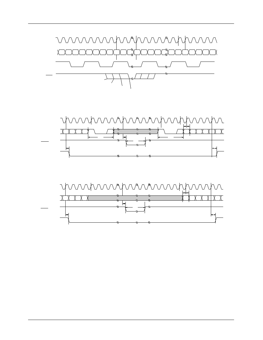
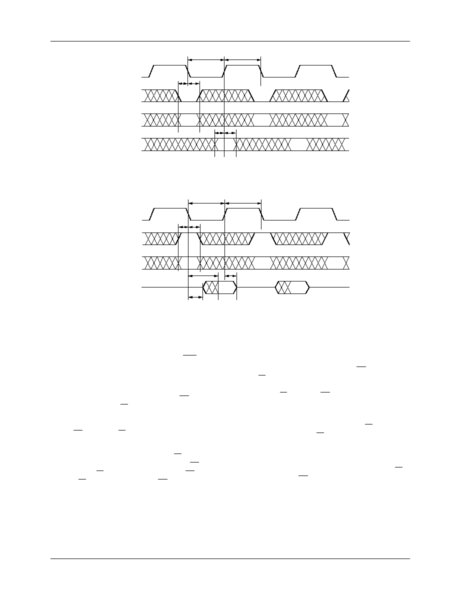
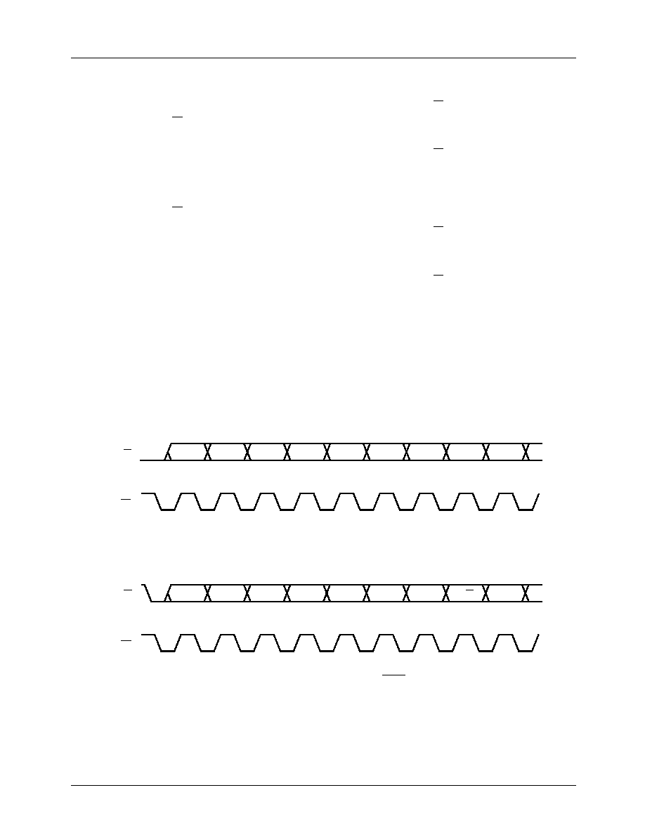
Horizontal and Vertical Timing
Horizontal and vertical video timing in the TMC2490A is
preprogrammed for line-locked systems with a 2x pixel
clock of 27.0 MHz.
Table 3 and Table 4 show timing parameters for NTSC and
PAL standards and the resulting TMC2490A analog output
timing. The user provides exactly 720 pixels of active video
per line. In master mode, the TMC2490A precisely controls
the duration and activity of every segment of the horizontal
line and vertical field group. In external sync slave mode, it
holds the end-of-line blank state (e.g. front porch for active
video lines) until it receives the next horizontal sync signal.
In CCIR-656 slave mode, it likewise holds each end-of-line
blank state until it receives the next end of active video
(EAV) signal embedded in the incoming data stream.
The vertical field group comprises several different line
types based upon the Horizontal line time.
H
= (2 x SL) + (2 x SH) [Vertical sync pulses]
= (2 x EL) + (2 x EH) [Equalization pulses]
SMPTE 170M NTSC and Report 624 PAL video standards
call for specific rise and fall times on critical portions of the
video waveform. The chip does this automatically, requiring
no user intervention. The TMC2490A digitally defines
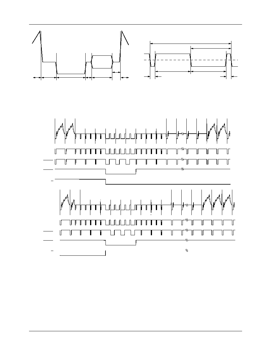
Figure 2a. HDEL TIming
Figure 2b. CCIR-656 Horizontal Interval Timing Detail
Figure 3. Master Mode Horizontal Interval Timing Detail
PXCK
PD
7-0
C
B732
Y
732
C
R732
Y
733
CBSEL
HYSNC
1464
1472
1592
1600
65-2490A-03
625-line
525-line
C
B734
Y
734
C
R734
Y
735
C
B736
Y
736
HDEL = 00
HDEL = 01
HDEL = 10
HDEL = 11
C
R736
C
B800
Y
800
C
R800
Y
801
C
B801
C
R856
Y
857
C
B0
Y
0
C
R0
Y
1
C
B2
0
0
1727
1715
PXCK
PD
7-0
1430
1435
FF
FF
00
00
FV
1
HSYNC (Output)
HDEL = 2
PDC
00
00
FV
0
C
B0
Y
0
1440
1440
1464
1472
1724
1712
t
DO
t
HP
t
SP
1727
1715
17
3
0
0
65-2490A-04
625-line
525-line
t
DO
t
DO
t
HS
SAV
EAV
PXCK
PD
7-0
1430
1435
HSYNC (Output)
HDEL = 2
PDC
C
B0
Y
0
1440
1440
1464
1472
17
3
t
DO
t
H
t
S
1727
1715
0
0
65-2490A-05
625-line
525-line
t
DO
t
DO
t
HS
PRODUCT SPECIFICATION
TMC2490A
13
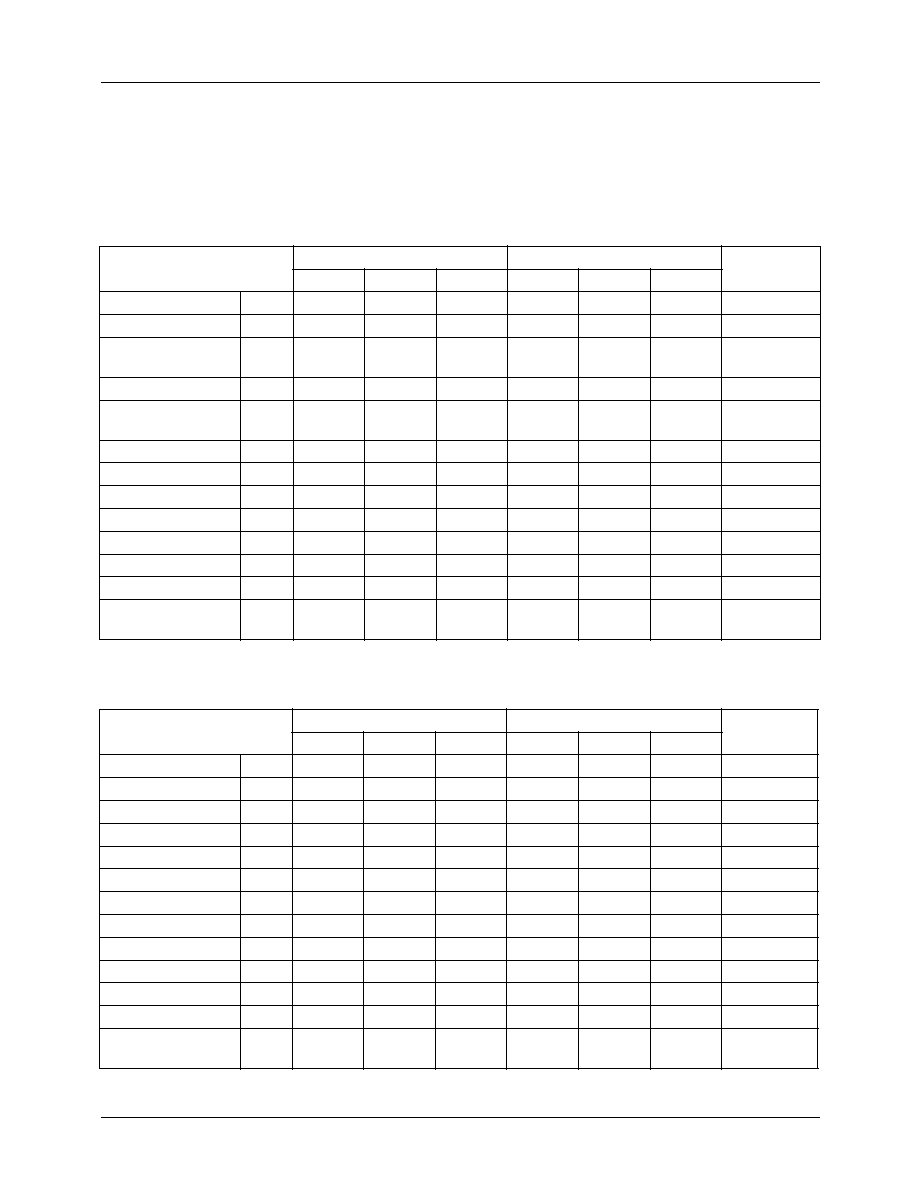
Table 3. Horizontal Timing Standards and Actual Values for 60 fps Video Standards (
µs)
Table 4. Horizontal Timing Standards and Actual Values for 50 fps Video Standards (
µs)
Parameter
NTSC (SMPTE 170M)
PAL-M (CCIR 624)
Min
Nom
Max
Min
Nom
Max
TMC2490A
Front porch
FP
1.4
1.5
1.6
1.27
2.22
1.53
Horiz. Sync
SY
4.6
4.7
4.8
4.6
4.7
4.8
4.74
Breezeway
BR
0.608
0.9
1.1
1.3
0.59 (NTSC)
1.04 (PAL-M)
Color Burst
BU
2.235
2.514
2.794
2.237
2.517
2.797
2.31
Color Back porch
CBP
1.378
0.503
2.363
1.65 (NTSC)
0.89 (PAL-M)
Blanking
BL
10.5
10.7
11.0
10.7
10.9
11.1
10.8
Active Video
VA
52.56
52.86
53.06
52.46
52.66
52.86
52.633
Line Time
H
63.556
63.556
63.557
Equalization HIGH
EH
29.5
29.5
29.47
Equalization LOW
EL
2.3
2.3
2.31
Sync HIGH
SH
4.7
4.7
4.67
Sync LOW
SL
27.1
27.1
27.13
Sync rise and fall
times
140
±20ns
<250 ns
135ns
Parameter
PAL-B,G,H,I (CCIR 624)
PAL-N (CCIR 624)
Min
Nom
Max
Min
Nom
Max
TMC2490A
Front porch
FP
1.2
1.5
1.8
1.2
1.5
1.8
1.57
Horiz. Sync
SY
4.5
4.7
4.9
4.5
4.7
4.9
4.74
Breezeway
BR
0.6
0.9
1.2
0.6
0.9
1.2
0.89
Color Burst
BU
2.030
2.255
2.481
2.233
2.513
2.792
2.3
Color Back porch
CBP
2.654
2.387
2.3
Blanking
BL
11.7
12.0
12.3
11.7
12.0
12.3
1.8
Active Video
VA
51.7
52.0
52.3
51.7
52.0
52.3
52.2
Line Time
H
64
64
64.0
Equalization HIGH
EH
29.65
29.65
29.63
Equalization LOW
EL
2.35
2.35
2.37
Sync HIGH
SH
4.7
4.7
4.67
Sync LOW
SL
27.3
27.3
27.3
Sync rise and fall
times
250
±50
ns
200
±100
ns
250
slopes compatible with SMPTE 170M NTSC or CCIR
Report 624 PAL on all vital edges:
1.
Sync leading and trailing edges.
2.
Burst envelope.
3.
Active video leading and trailing edges.
4.
All vertical interval equalization pulse and sync edges.
TMC2490A
PRODUCT SPECIFICATION
14
REV. 1.0.2 2/27/02
Figure 4. Horizontal Blanking Interval Timing
Figure 5. Vertical Sync and Equalization Pulse Detail
BURST
CBP
VA
24318B
BU
BR
SY
FP
VA
H/2
SL
EH
EL
SH
24319A
H
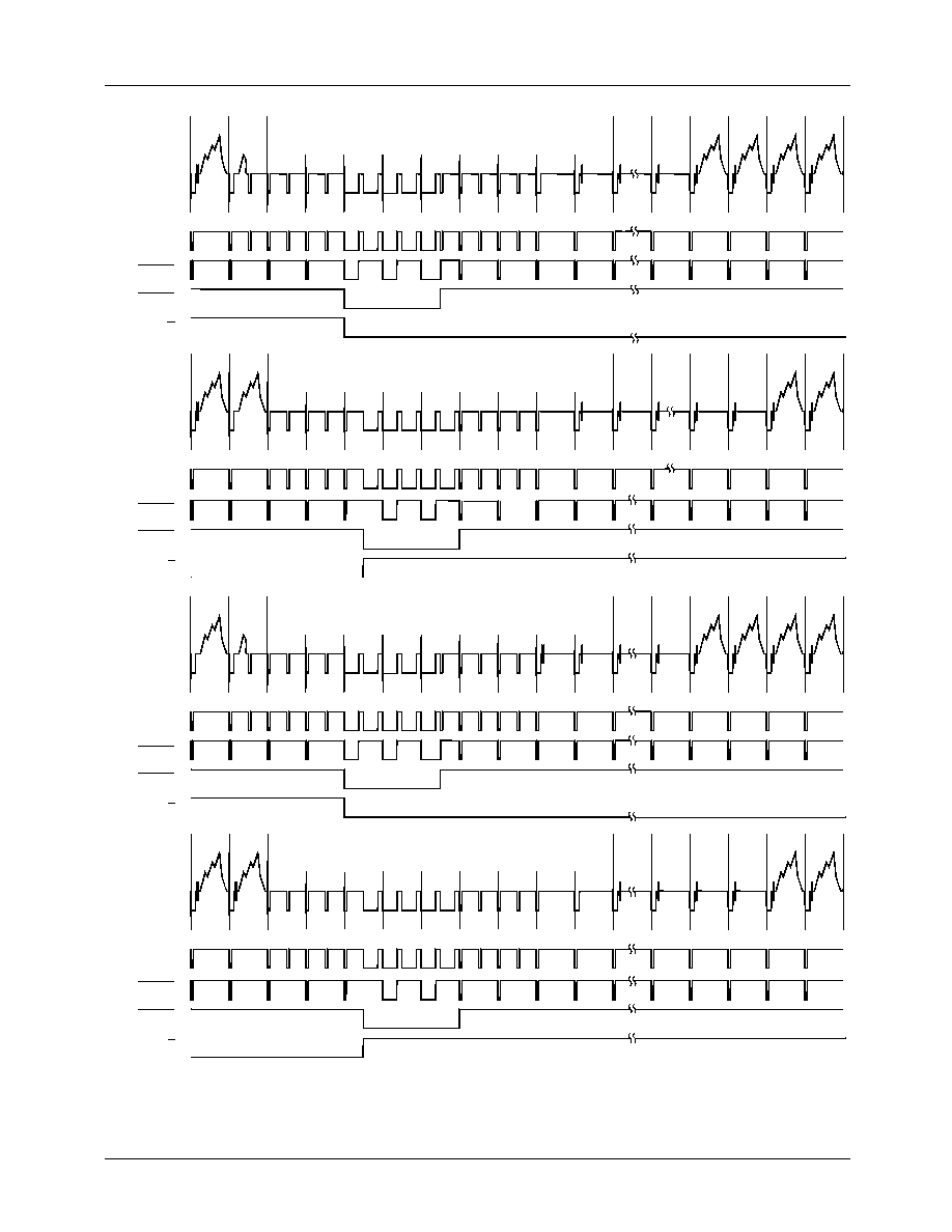
Figure 6. NTSC Vertical Interval
FIELDS 1 AND 3
FIELDS 2 AND 4
525
EE
EE
EE
SS
SS
SS
EE
EE
EB
10
...
19
20
21
22
UBB
UBB
UBB
UVV
UVV
524
UVV
UVV
UVV
UVE
EE
EE
ES
SS
SS
SE
EE
EE
EB
264
265
266
267
268
269
270
271
272
UBB
UBB
UVV
UVV
UVV
262
263
273
...
282
283
284
285
COMPOSITE
SYNC
24492B
B/T
HSYNC
VSYNC
COMPOSITE
SYNC
HSYNC
VSYNC
B/T

PRODUCT SPECIFICATION
TMC2490A
15
Table 6. NTSC Field/Line Sequence and Identification
EE Equalization pulse
EB
Equalization broad pulse
SE Half-line vertical sync pulse, half-line equalization pulse
UBB
Black and Burst
1
SS Vertical sync pulse
UVV
Active video
ES Half-line equalization pulse, half-line vertical sync pulse
UVE
Half-line video, half-line equalization pulse
Note:
1. VBB lines are changed to UVV (Active Video) when VBIEN = 1.
Field 1, FID = 00
Field 2, FID = 01
Field 3, FID = 10
Field 4, FID = 11
Line
ID
Line
ID
Line
ID
Line
ID
1
EE
264
EE
1
EE
264
EE
2
EE
265
EE
2
EE
265
EE
3
EE
266
ES
3
EE
266
ES
4
SS
267
SS
4
SS
267
SS
5
SS
268
SS
5
SS
268
SS
6
SS
269
SE
6
SS
269
SE
7
EE
270
EE
7
EE
270
EE
8
EE
271
EE
8
EE
271
EE
9
EE
272
EB
9
EE
272
EB
10
UBB
273
UBB
10
UBB
273
UBB
...
...
...
...
...
...
...
...
20
UBB
282
UBB
20
UBB
282
UBB
21
UVV
283
UVV
10
UVV
273
UVV
...
...
...
...
...
...
...
...
262
UVV
524
UVV
262
UVV
524
UVV
263
UVE
525
UVV
263
UVE
525
UVV
TMC2490A
PRODUCT SPECIFICATION
REV. 1.0.2 2/27/02
16
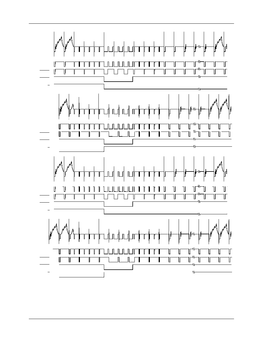
Figure 7. PAL-B,G,H,I,N Vertical Interval
COMPOSITE
SYNC
1247
1249
1
2
3
4
5
EE
EE
SS
SS
SE
EE
EE
6
7
...
22
23
24
25
26
1248
UVV
-BB
UBB
...
UBB
UVV
UVV
UVV
UVV
-VE
FIELDS 1 AND 5
B/T
HSYNC
VSYNC
COMPOSITE
SYNC
309
311
312
313
314
315
316
317
318
EE
EE
ES
SS
SS
EE
EE
319
320
...
334
335
336
337
310
UVV
EB
UBB
UBB
...
UBB
UBB
UVV
UVV
-VV
FIELDS 2 AND 6
B/T
HSYNC
VSYNC
COMPOSITE
SYNC
622
624
625
626
627
628
629
630
631
EE
EE
SS
SS
SE
EE
EE
632
...
647
648
649
650
651
623
-VV
UBB
UBB
...
UBB
UVV
UVV
UVV
UVV
-VE
FIELDS 3 AND 7
B/T
HSYNC
VSYNC
COMPOSITE
SYNC
934
936
937
938
939
940
941
942
943
EE
EE
ES
SS
SS
EE
EE
944
945
...
959
960
961
962
935
UVV
EB
-BB
UBB
...
UBB
UBB
24495B
UVV
UVV
UVV
FIELDS 4 AND 8
B/T
HSYNC
VSYNC

PRODUCT SPECIFICATION
TMC2490A
17
Table 7. PAL-B,G,H,I,N Field/Line Sequence and Identification
EE Equalization pulse
UBB
Black and Burst
1
SE Half-line vertical sync pulse, half-line equalization pulse
UVV
Active video
SS Vertical sync pulse
-BB
Blank line with color burst suppression
2
ES Half-line equalization pulse, half-line vertical sync pulse
-VV
Active video with color burst suppressed
EB Equalization broad pulse
-VE
Half-line video, half-line equalization pulse,
color burst suppressed
Notes:
1. VBB lines are changed to UVV (Active Video) when VBIEN = 1.
2. -BB lines are changed to -VV (Active Video, Burst Suppressed) when VBIEN = 1.
Fields 1 and 5
FID = 000, 100
Fields 2 and 6
FID = 001, 101
Fields 3 and 7
FID = 010, 110
Fields 4 and 8
FID = 011, 111
Line
ID
Line
ID
Line
ID
Line
ID
1
SS
313
ES
626
SS
938
ES
2
SS
314
SS
627
SS
939
SS
3
SE
315
SS
628
SE
940
SS
4
EE
316
EE
629
EE
941
EE
5
EE
317
EE
630
EE
942
EE
6
-BB
318
EV
631
UBB
943
EB
7
UBB
319
UBB
632
UBB
944
-BB
8
UBB
320
UBB
633
UBB
945
UBB
...
...
...
...
...
...
...
...
22
UBB
335
UBB
647
UBB
960
UBB
23
UVV
336
UVV
648
UVV
961
UVV
...
...
...
...
...
...
...
...
308
UVV
621
UVV
933
UVV
1246
UVV
309
UVV
622
-VV
934
UVV
1247
UVV
310
-VV
623
-VE
935
UVV
1248
-VE
311
EE
624
EE
936
EE
1249
EE
312
EE
625
EE
937
EE
1250
EE
TMC2490A
PRODUCT SPECIFICATION
REV. 1.0.2 2/27/02
18
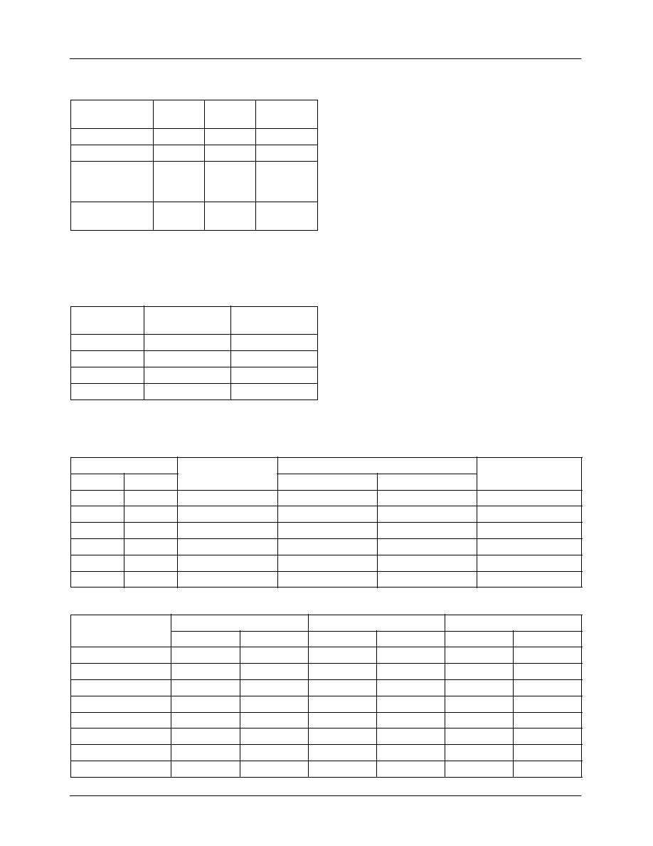
Figure 8. PAL-M Vertical Interval
COMPOSITE
SYNC
521
523
524
525
1
2
3
4
EE
EE
EE
SS
SS
SS
EE
5
6
7
8
9
...
17
18
522
UVV
EE
EE
-BB
-BB
UBB
...
UBB
UVV
UVV
FIELDS 1 AND 5
B/T
HSYNC
VSYNC
COMPOSITE
SYNC
521
523
524
525
1
2
3
4
EE
EE
EE
SS
SS
SS
EE
5
6
7
8
9
...
17
18
522
UVV
EE
EE
-BB
-BB
UBB
...
UBB
UVV
-VV
FIELDS 3 AND 7
B/T
HSYNC
VSYNC
COMPOSITE
SYNC
259
261
262
263
264
265
266
267
EE
EE
ES
SS
SS
SE
EE
268
269
270
271
...
279
280
281
260
UVV
EE
EB
-BB
UBB
...
UBB
UVV
UVV
-VE
FIELDS 2 AND 6
B/T
HSYNC
VSYNC
COMPOSITE
SYNC
259
261
262
263
264
265
266
267
EE
EE
ES
SS
SS
SE
EE
268
269
270
271
...
279
280
281
24496B
260
-VV
258
UVV
EE
EB
-BB
UBB
...
UBB
UVV
UVV
-VE
FIELDS 4 AND 8
B/T
HSYNC
VSYNC

PRODUCT SPECIFICATION
TMC2490A
REV. 1.0.2 2/27/02
19
Subcarrier Generation and Synchronization
The color subcarrier is generated by an internal digital
frequency synthesizer. The subcarrier synthesizer gets its
frequency and phase values preprogrammed into the
TMC2490A.
In Master Mode, the subcarrier is internally synchronized on
field 1 of the eight-field sequence to establish and maintain a
specific relationship between the leading edge of horizontal
sync and color burst phase (SCH). Proper subcarrier phase is
maintained through the entire eight field set, including the 25
Hz offset in PAL-N/B/I systems. The subcarrier is reset to
the phase values found in Table 9.
SCH Phase Control
SCH refers to the timing relationship between the 50% point
of the leading edge of horizontal sync and the first positive or
negative zero-crossing of the color burst subcarrier refer-
ence. In PAL, SCH is defined for line 1 of field 1, but since
there is no color burst on line 1, SCH is usually measured at
line 7 of field 1. The need to specify SCH relative to a partic-
ular line in PAL is due to the 25 Hz offset of PAL subcarrier
frequency. Since NTSC has no such 25 Hz offset, SCH
applies to all lines.
Table 8. PAL-M Field/Line Sequence and Identification
EE Equalization pulse
UBB
Black and Burst
1
SE Half-line vertical sync pulse, half-line equalization pulse
UVV
Active video
SS Vertical sync pulse
-BB
Blank line with color burst suppression
2
ES Half-line equalization pulse, half-line vertical sync pulse
-VV
Active video with color burst suppressed
EB Equalization broad pulse
UVV
Half-line black, half-line video
-VEHalf-line video, half-line equalization pulse,
color burst suppressed
Notes:
1. VBB lines are changed to UVV (Active Video) when VBIEN = 1
2. -BB lines are changed to -VV (Active Video, Burst Suppressed) when VBIEN = 1
Field 1 and 5
FID = 000, 100
Field 2 and 6
FID = 001, 101
Field 3 and 7
FID = 010, 110
Field 4 and 8
FID = 011, 111
Line
ID
Line
ID
Line
ID
Line
ID
1
SS
263
ES
1
SS
263
ES
2
SS
264
SS
2
SS
264
SS
3
SS
265
SS
3
SS
265
SS
4
EE
266
SE
4
EE
266
SE
5
EE
267
EE
5
EE
267
EE
6
EE
268
EE
6
EE
268
EE
7
-BB
269
EB
7
-BB
269
EB
8
-BB
270
-BB
8
UBB
270
-BB
9
UBB
271
UBB
9
UBB
271
UBB
...
...
...
...
...
...
...
...
17
UBB
279
UBB
17
UBB
279
UBB
18
UVV
280
UVV
18
UVV
280
UVV
...
...
...
...
...
...
...
...
258
UVV
521
UVV
258
UVV
521
UVV
259
UVV
522
-VV
259
-VV
522
UVV
260
-VE
523
EE
260
-VE
523
EE
261
EE
524
EE
261
EE
524
EE
262
EE
525
EE
262
EE
525
EE
TMC2490A
PRODUCT SPECIFICATION
20
REV. 1.0.2 2/27/02
Table 9. Subcarrier and Color Burst Reset
Values
Note:
1. Line numbering is in accordance with Figure 6, Figure 7,
and Figure 8. Subcarrier and color burst phase are relative
to the horizontal reference of the line specified above.
Table 10. Standard Subcarrier Parameters
NTSC
PAL-M
PAL-
B,G,H,I,N
Digital field:
1
1
1
Line number:
4
4
1
Subcarrier
phase reset
value:
180
°
0
°
0
°
Resultant color
burst phase:
0
°
+135
°
+135
°
Standard
Horizontal
Frequency (KHz)
Subcarrier
Frequency (MHz)
NTSC
15.734266
3.579545455
PAL B,G,H,I
15.625000
4.43361875
PAL-M
15.734266
3.57561189
PAL-N
15.625000
3.58205625
Luminance Processing
During horizontal and vertical blanking, the luma processor
generates blanking levels and properly timed and shaped
sync and equalization pulses. During active video, it captures
and rescales the incoming Y components and adds the results
to the blank level to complete a proper monochrome televi-
sion waveform, which is then upsampled to drive the luma
D/A and the composite adder.
For NTSC-EIA (5:2 white:sync, no black pedestal), the over-
all luma input-to-output equation for 0<Y<255 is:
luma out (IRE, relative to blank) = (Y - 16) * 100/219
For NTSC and PAL-M (5:2, with 7.5 IRE pedestal), the
equation becomes:
luma out (IRE, relative to blank) = (Y - 16) * 92.5/219 + 7.5
For all 625-line PAL standards (7:3, no pedestal), the equa-
tion becomes:
luma out (mV, relative to blank) = (Y-16) * 700/219
Since Y=0 and Y=255 are reserved values in CCIR-601,
results in the luma D/A outputting black, i.e., 0mV or 0 IRE
without pedestal, 7.5 IRE with pedestal. External compo-
nents are needed to bias the blanking/black level to 0mV/0
IRE. The values given in Table 11 and Table 12 reflect a
biased output where the blanking level is at 0mV/0 IRE.
Table 11. Luminance Input Codes
Table 12. D/A Converter and Analog Levels
PD
7-0
Input
Luma Level
(CCIR-601)
NTSC, PAL-M Luma Level (IRE)
PAL-B,G,H,I,N
Luma Level (mV)
Dec
Hex
PEDEN = 0
PEDEN = 1
255
FF
Reserved
0
7.5
0
254
FE
108.7
108
761
235
EB
100% white
100
100
700
16
10
Black
0
7.5
0
1
01
-6.9
1.2
-48
0
00
Reserved
0
7.5
0
Video Level
NTSC, PAL-M
NTSC w/o Setup
PAL-B,G,H,I,N
D/A
IRE
D/A
IRE
D/A
mV
Maximum Output
1022
134.8
1022
138.4
1022
817
100% white
820
100
820
100
800
700
Black
284
7.5
240
0
240
0
Blank
240
0
240
0
240
0
Sync
12
-40
12
-40
0
-300
White-to-blank
580
100
580
100
560
700
White-to- sync
808
140
808
140
800
1000
Color burst p-p
232
40
232
40
244
300
PRODUCT SPECIFICATION
TMC2490A
REV. 1.0.2 2/27/02
21
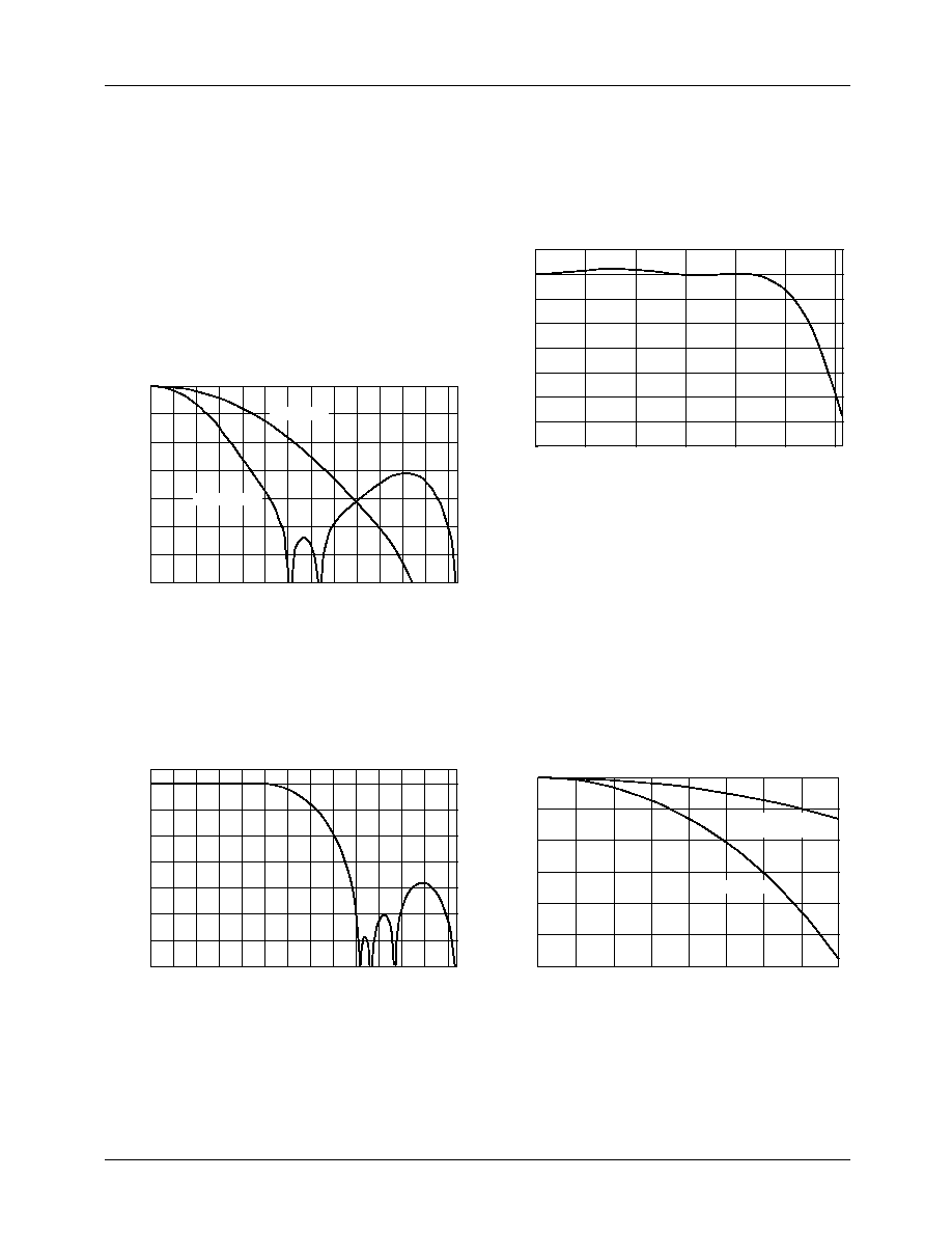
Filtering Within the TMC2490A
The TMC2490A incorporates internal digital filters to estab-
lish appropriate bandwidths and simplify external analog
reconstruction filter designs.
The chroma portion of the incoming digital video is band-
limited to reduce edge effect and other distortions of the
image compression process. Chrominance bandwidth is
selected by CHRBW. When LOW, the chrominance pass-
band attenuation is <3 dB within
±650 kHz from f
SC
. The
stopband rejection is >26 dB outside f
SC
±2 MHz. When
HIGH, the chrominance passband attenuation is <3 dB
within
±1.3 MHz from f
SC
. The stopband rejection is
>33 dB outside f
SC
±4 MHz.
Figure 9. Color-Difference Low-Pass Filter Response
The Chroma Modulator output and the luminance data are
digitally filtered with sharp-cutoff low-pass interpolation fil-
ters. These filters ensure that aliased subcarrier, chromi-
nance, and luminance frequencies are sufficiently suppressed
above the video base-band.
Figure 10. Chrominance and Luminance Interpolation
Filter Full Spectrum Response
-70
-60
-50
-40
-30
-20
-10
0
0.0 0.5 1.0 1.5 2.0 2.5 3.0 3.5 4.0 4.5 5.0 5.5 6.0 6.5
Frequency (MHz)
Attenuation (dB)
24490A
Wideband
Narrowband
-70
-60
-50
-40
-30
-20
-10
0
0
1
2
3
4
5
6
7
8
9
10 11 12 13
Frequency (MHz)
Attenuation (dB)
24487A
Virtually all digital-to-analog converters have a response
with high frequency roll-off as a result of the zero-order hold
characteristic of classic D/A converters. This response is
commonly referred to as a sin(x)/x response. The sin(x)/x vs.
sampling frequency is shown in Figure 12.
Figure 11. Chrominance and Luminance Interpolation
Filter Passband Detail
The TMC2490A's digital interpolation filters convert the
data stream to a sample rate of twice the pixel rate. This
results in much less high frequency sin(x)/x rolloff and the
output spectrum between f
S
/4 and 3 x f
S
/4 contains very lit-
tle energy. Since there is so little signal energy in this fre-
quency band, the demands placed on the output
reconstruction filter are greatly reduced. The output filter
needs to be flat to f
S
/4 and have good rejection at 3 x f
S
/4.
The relaxed requirements greatly simplify the design of a fil-
ter with good phase response and low group delay distortion.
A small amount of peaking may be added to compensate
residual sin(x)/x rolloff.
Figure 12. Sin(x)/x Response
-3.5
-3.0
-2.5
-2.0
-1.5
-1.0
-0.5
0.0
0.5
0
1
2
3
4
5
6
Frequency (MHz)
Attenuation (dB)
24488A
-6
-5
-4
-3
-2
-1
0
0
1
2
3
4
5
6
7
8
Fs=13.5Msps
Fs=27.0Msps
(Oversampled)
Frequency (MHz)
Attenuation (dB)
24489A
TMC2490A
PRODUCT SPECIFICATION
22
REV. 1.0.2 2/27/02
Closed Caption Insertion
The TMC2490A includes a flexible closed caption processor.
It may be programmed to insert a closed caption signal on
any line within a range of 16 lines on ODD and/or EVEN
fields.
Closed Caption insertion overrides all other configurations
of the encoder. If it is specified on an active video line, it
takes precedence over the video data and removes NTSC
setup if setup has been programmed for the active video
lines.
Closed Caption Control
Closed caption is turned on by setting CCON HIGH. When-
ever the encoder begins producing a line specified by
CCFLD and CCLINE, it will insert a closed caption line in
its place. If CCRTS is HIGH, the data contained in CCDx
will be sent. IF CCRTS is LOW, Null Bytes (hex 00 with
ODD parity) will be sent.
Line Selection
The line to contain CC data is selected by a combination of
the CCFLD bit and the CCLINE bits. CCLINE is added to
the offset shown in Table 13 to specify the line.
Table 13. Closed Caption Line Selection
Parity Generation
Standard Closed-Caption signals employ ODD parity, which
may be automatically generated by setting CCPAR HIGH.
Alternatively, parity may be generated externally as part of
the bytes to be transmitted, and, with CCPAR LOW, the
entire 16 bits loaded into the CCDx registers will be sent
unchanged.
Operating Sequence
A typical operational sequence for closed-caption insertion
on Line 21 is:
1.
Read Register 22 and check that bit 6 is LOW, indicat-
ing that the CCDx registers are ready to accept data.
2.
If ready, write two bytes of CC data into registers 20 and
21.
Standard
Offset
Field
Lines
525
12
ODD
12-27
274
EVEN
274-289
625
9
ODD
9-24
321
EVEN
321-336
3.
Write into register 22 the proper combination of CCFLD
and CCLINE. CCPAR may be written as desired. Set
CCRTS HIGH.
4.
The CC data is transmitted during the specified line.
As soon as CCDx is transferred into the CC processor (and
CCRTS goes LOW), new data may be loaded into registers
20 and 21. This allows the user to transmit CC data on sev-
eral consecutive lines by loading data for line n+1 while data
is being sent on line n.
Registers 20-21 auto-increment when read or written. Regis-
ter 22 does not. The microcontroller can repeatedly read
register 22 until CCRTS is found to be LOW, then address
register 20 and write three auto-incremented bytes to set up
for the next CC line.
Parallel Microprocessor Interface
The parallel microprocessor interface, active when SER is
HIGH, employs an 11-line interface, with an 8-bit data bus
and one address bit: two addresses are required for device
programming and pointer-register management. Address bit
0 selects between reading/writing the register addresses and
reading/writing register data. When writing, the address is
presented along with a LOW on the R/W pin during the fall-
ing edge of CS. Eight bits of data are presented on D
7-0
dur-
ing the subsequent rising edge of CS.
In read mode, the address is accompanied by a HIGH on the
R/W pin during a falling edge of CS. The data output pins go
to a low-impedance state t
DOZ
ns after CS falls. Valid data is
present on D
7-0
t
DOM
after the falling edge of CS.
Table 14. Parallel Port Control
ADR
R/W
Action
1
0
Load D
7-0
into Control Register
pointer.
1
1
Read Control Register pointer on
D
7-0
.
0
0
Write D
7-0
to addressed Control
Register.
0
1
Read addressed Control Register
on D
7-0
.
PRODUCT SPECIFICATION
TMC2490A
REV. 1.0.2 2/27/02
23
Serial Control Port (R-Bus)
In addition to the 11-wire parallel port, a 2-wire serial con-
trol interface is also provided, and active when SER is LOW.
Either port alone can control the entire chip. Up to four
TMC2490A devices may be connected to the 2-wire serial
interface with each device having a unique address.
The 2-wire interface comprises a clock (SCL/CS) and a bi-
directional data (SDA/R/W) pin. The TMC2490A acts as a
slave for receiving and transmitting data over the serial inter-
face. When the serial interface is not active, the logic levels
on SCL/CS and SDA/R/W are pulled HIGH by external pull-
up resistors.
Data received or transmitted on the SDA/R/W line must be
stable for the duration of the positive-going SCL/CS pulse.
Data on SDA/R/W can only change when SCL/CS is LOW.
If SDA/R/W changes state while SCL/CS is HIGH, the serial
interface interprets that action as a start or stop sequence.
There are five components to serial bus operation:
· Start signal
· Slave address byte
· Base register address byte
· Data byte to read or write
· Stop signal
When the serial interface is inactive (SCL/CS and
SDA/R/W are HIGH) communications are initiated by send-
ing a start signal. The start signal is a HIGH-to-LOW transi-
tion on SDA/R/W while SCL/CS is HIGH. This signal alerts
all slaved devices that a data transfer sequence is coming.
The first eight bits of data transferred after a start signal com-
prise a seven bit slave address and a single R/W bit. As
shown in Figure 16A, the R/W bit indicates the direction of
data transfer, read from or write to the slave device. If the
transmitted slave address matches the address of the device
(set by the state of the SA
0
/ADR and SA
1
input pins in Table
15), the TMC2490A acknowledges by bringing SDA/R/W
LOW on the 9th SCL/CS pulse. If the addresses do not
match, the TMC2490A does not acknowledge.
Figure 13. Microprocessor Parallel Port - Write Timing
Figure 14. Microprocessor Parallel Port - Read Timing
t
PWLCS
t
HA
t
SA
t
HD
t
SD
t
PWHCS
SCL/
CS
SA
0
/ADR
65-3548-02
SDA / R/
W
D
7-0
t
SA
t
DOM
t
DOZ
t
HA
t
HOM
t
PWLCS
t
PWHCS
SCL/
CS
SA
0
/ADR
65-3548-03
SDA / R/
W
D
7-0
TMC2490A
PRODUCT SPECIFICATION
24
REV. 1.0.2 2/27/02
Table 15. Serial Port Addresses
Data Transfer via Serial Interface
For each byte of data read or written, the MSB is the first bit
of the sequence.
If the TMC2490A does not acknowledge the master device
during a write sequence, the SDA/R/W remains HIGH so the
master can generate a stop signal. If the master device does
not acknowledge the TMC2490A during a read sequence,
the TMC2490A interprets this as "end of data." The SDA/R/
W remains HIGH so the master can generate a stop signal.
Writing data to specific control registers of the TMC2490A
requires that the 8-bit address of the control register of inter-
est be written after the slave address has been established.
This control register address is the base address for subse-
quent write operations. The base address auto-increments by
one for each byte of data written after the data byte intended
for the base address. If more bytes are transferred than there
A
6
A
5
A
4
A
3
A
2
A
1
(SA
1
)
A
0
(SA
0
)
0
0
0
1
1
0
0
0
0
0
1
1
0
1
0
0
0
1
1
1
0
0
0
0
1
1
1
1
are available addresses, the address will not increment and
will remain at its maximum value of 22h. Any base address
higher than 22h will not produce an ACKnowledge signal.
Data is read from the control registers of the TMC2490A in a
similar manner. Reading requires two data transfer opera-
tions:
· The base address must be written with the R/W bit of the
slave address byte LOW to set up a sequential read
operation.
· Reading (the R/W bit of the slave address byte HIGH)
begins at the previously established base address. The
address of the read register auto-increments after each
byte is transferred.
To terminate a read/write sequence to the TMC2490A, a stop
signal must be sent. A stop signal comprises of a LOW-to-
HIGH transition of SDA/R/W while SCL/CS is HIGH.
A repeated start signal occurs when the master device driv-
ing the serial interface generates a start signal without first
generating a stop signal to terminate the current communica-
tion. This is used to change the mode of communication
(read, write) between the slave and master without releasing
the serial interface lines.
Figure 15. Serial Port Read/Write Timing
t
BUFF
t
DAL
t
DAH
t
STAH
t
DHO
SDA / R/
W
SCL/
CS
t
DSU
24469A
t
STOSU
t
STASU
PRODUCT SPECIFICATION
TMC2490A
REV. 1.0.2 2/27/02
25
Serial Interface Read/Write Examples
Write to one control register
· Start signal
· Slave Address byte (R/W bit = LOW)
· Base Address byte
· Data byte to base address
· Stop signal
Write to four consecutive control registers
· Start signal
· Slave Address byte (R/W bit = LOW)
· Base Address byte
· Data byte to base address
· Data byte to (base address + 1)
· Data byte to (base address + 2)
· Data byte to (base address + 3)
· Stop signal
Read from one control register
· Start signal
· Slave Address byte (R/W bit = LOW)
· Base Address byte
· Stop signal
· Start signal
· Slave Address byte (R/W bit = HIGH)
· Data byte from base address
· No Acknowledge
Read from four consecutive control registers
· Start signal
· Slave Address byte (R/W bit = LOW)
· Base Address byte
· Stop signal
· Start signal
· Slave Address byte (R/W bit = HIGH)
· Data byte from base address
· Data byte from (base address + 1)
· Data byte from (base address + 2)
· Data byte from (base address + 3)
· No Acknowledge
Figure 16. Serial Interface Typical Byte Transfer
Figure 16A. Chip Address with Read/Write Bit
24470A
MSB
LSB
ACK
SCL/CS
SDA / R/W
65-3548-05
A
6
A
5
A
4
A
3
A
2
SA
1
SA
0
R/W
ACK
SCL/CS
SDA / R/W
TMC2490A
PRODUCT SPECIFICATION
REV. 1.0.2 2/27/02
26
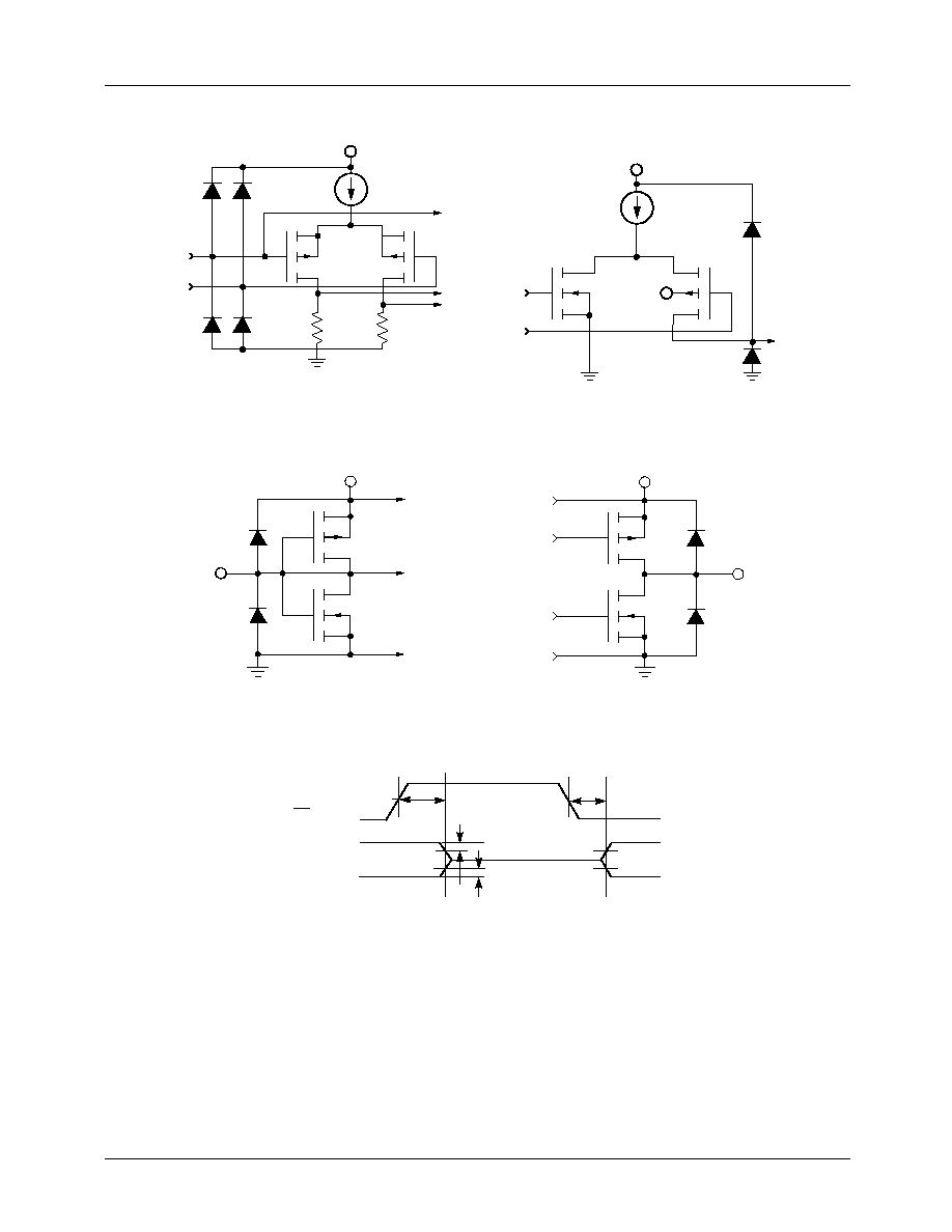
Equivalent Circuits and Threshold Levels
Figure 18. Equivalent Analog Input Circuit
Figure 19. Equivalent Analog Output Circuit
Figure 20. Equivalent Digital Input Circuit
Figure 21. Equivalent Digital Output Circuit
Figure 22. Threshold Levels for Three-State Measurements
p
GND
27012B
R
REF
V
REF
V
DD
p
n
p
OUT
GND
27013B
V
DD
V
DD
Digital
Input
V
DD
p
n
27014C
GND
V
DD
p
n
27011C
GND
Digital
Output
7048C
t
ENA
2.0V
0.8V
t
DIS
Three-State
Outputs
CS
High Impedance
0.5V
0.5V
PRODUCT SPECIFICATION
TMC2490A
27
Absolute Maximum Ratings
(beyond which the device may be damaged)
1
Notes:
1. Functional operation under any of these conditions is NOT implied. Performance and reliability are guaranteed only if
Operating Conditions are not exceeded.
2. Applied voltage must be current limited to specified range.
3. Forcing voltage must be limited to specified range.
4. Current is specified as conventional current flowing into the device.
Parameter
Min.
Typ.
Max.
Unit
Power Supply Voltage
-0.5
7.0
V
Digital Inputs
Applied Voltage
2
-0.5
V
DD
+ 0.5
V
Forced Current
3,4
-20.0
20.0
mA
Output
Applied Voltage
2
-0.5
V
DD
+ 0.5
V
Forced Current
3,4
-3.0
6.0
mA
Short Circuit Duration (single output in HIGH state to ground)
1
sec
Analog Short Circuit Duration (all outputs to ground)
Infinite
Temperature
Operating, Ambient
-20
110
°C
Junction
140
°C
Storage Temperature
-65
150
°C
Lead Soldering (10 seconds)
300
°C
Vapor Phase Soldering (1 minute)
220
°C
Operating Conditions
Parameter
Conditions
Min.
Typ.
Max.
Units
V
DD
Power Supply Voltage
4.75
5.0
5.25
V
V
IH
Input Voltage, Logic HIGH
TTL Compatible Inputs
2.0
V
DD
V
CLK Input
2.4
V
DD
R-Bus Inputs
0.7V
DD
V
IL
Input Voltage, Logic LOW
TTL Compatible Inputs
GND
0.8
V
R-Bus Inputs
0.3V
DD
V
REF
External Reference Voltage
1.235
V
I
REF
D/A Converter Reference Current
(I
REF
= V
REF
/R
REF
),
flowing out of the R
REF
pin
1.57
mA
R
REF
External Reference Resistor
V
REF
= NOM, R
L
= 75
787
I
OH
Output Current, Logic HIGH
-2.0
mA
I
OL
Output Current, Logic LOW
4.0
mA
T
A
Ambient Temperature, Still Air
0
70
°C
TMC2490A
PRODUCT SPECIFICATION
REV. 1.0.2 2/27/02
28
Pixel Interface
f
PXL
Pixel Rate
13.5
Mpps
f
PXCK
Master Clock Rate
= 2X pixel rate
27.0
MHz
t
PWHPX
PXCK pulse width, HIGH
10
ns
t
PWLPX
PXCK pulse width, LOW
15
ns
t
SP
PD
7-0
Setup Time
15
ns
t
HP
PD
7-0
Hold Time
0
ns
Parallel Microprocessor Interface
t
PWLCS
CS Pulse Width, LOW
95
ns
t
PWHCS
CS Pulse Width, HIGH
3
pixels
t
SA
Address Setup Time
17
ns
t
HA
Address Hold Time
0
ns
t
SD
Data Setup Time (write)
17
ns
t
HD
Data Hold Time (write)
0
ns
t
PWLR
RESET Pulse Width, LOW
16
PXCK
Serial Microprocessor Interface
t
DAL
SCL Pulse Width, LOW
1.3
µs
t
DAH
SCL Pulse Width, HIGH
0.6
µs
t
STAH
SDA Start Hold Time
0.6
µs
t
STASU
SCL to SDA Setup Time (Stop)
0.6
µs
t
STOSU
SCL to SDA Setup Time (Start)
0.6
µs
t
BUFF
SDA Stop Hold Time Setup
1.3
µs
t
DSU
SDA to SCL Data Setup Time
300
ns
t
DHO
SDA to SCL Data Hold Time
300
ns
Operating Conditions
(continued)
Parameter
Conditions
Min.
Typ.
Max.
Units
PRODUCT SPECIFICATION
TMC2490A
29
DC Electrical Characteristics
Notes:
1. Maximum I
DD
with V
DD
= Max and T
A
= Min. Outputs loaded wtih 75
.
2. I
DDQ
when RESET = LOW, disabling D/A converters.
AC Electrical Characteristics
Note:
1. Timing reference points are at the 50% level. Analog C
LOAD
<10pF, D
7-0
load <40pF.
Parameter
Conditions
Min.
Typ.
Max.
Units
I
DD
Power Supply Current, Unloaded
1
V
DD
= Max, f
PXCK
= 27MHz
130
mA
I
DDQ
Power Supply Current, Quiescent
2
V
DD
= Max
20
mA
V
RO
Voltage Reference Output
1.173
1.235
1.297
V
I
BR
Reference Bias
-100
100
µA
Z
RO
V
REF
Output Impedance
1000
I
IH
Input Current, HIGH
V
DD
= Max, V
IN
= V
DD
±10
µA
I
IL
Input Current, LOW
V
DD
= Max, V
IN
= 0V
±10
µA
I
OZH
Hi-Z Output Leakage Current,
Output HIGH
V
DD
= Max, V
IN
= V
DD
±10
µA
I
OZL
Hi-Z Output Leakage Current,
Output LOW
V
DD
= Max, V
IN
= 0V
±10
µA
I
OS
Short-Circuit Current
-50
-10
mA
V
OH
Output Voltage, HIGH
I
OH
= Max
2.4
V
V
OL
Output Voltage, LOW
I
OL
= Max
0.4
V
C
I
Digital Input Capacitance
4
10
pF
C
I
Digital Output Capacitance
10
pF
V
OC
Video Output Compliance
-0.3
2.0
V
R
OUT
Video Output Resistance
15
k
C
OUT
Video Output Capacitance
I
OUT
= 0mA, f = 1MHz
15
25
pF
Parameter
Conditions
Min.
Typ.
Max.
Units
t
DOZ
Output Delay, CS to low-Z
14
ns
t
HOM
Output Hold Time, CS to high-Z
30
ns
t
DOM
Output Delay, CS to Data Valid
40
ns
t
R
D/A Output Current Risetime
10% to 90% of full scale
2
ns
t
F
D/A Output Current Falltime
90% to 10% of full scale
2
ns
t
DOV
Analog Output Delay
3
11
17
ns
TMC2490A
PRODUCT SPECIFICATION
REV. 1.0.2 2/27/02
30
System Performance Characteristics
Note:
1. Noise Level is uniformly weighted, 10 kHz to 5.0 MHz bandwidth, with Tilt Null ON measured using VM700 "Measure Mode."
Parameter
Conditions
Min.
Typ.
Max.
Units
RES
D/A Converter Resolution
10
10
10
Bits
dp
Differential Phase
PXCK = 27 MHz,
40 IRE Ramp
0.6
degree
dg
Differential Gain
PXCK = 27 MHz,
40 IRE Ramp
0.7
%
CNLP
Chroma Nonlinear Phase
NTC-7 Combination
0.3
degree
CNLG
Chroma Nonlinear Gain
NTC-7 Combination
TBD
%
CLIM
Chroma/Luma Intermodulation
NTC-7 Combination
0.3
IRE
CLGI
Chroma/Luma Gain inequality
NTC-7 Composite
TBD
%
CLDI
Chroma/Luma Delay inequality
NTC-7 Composite
7.1
ns
LNLD
Luma Nonlinear Distortion
NTC-7
TBD
%
FTWD
Field Time Waveform Distortion
NTC-7
0.1
%
LTWD
Line Time Waveform Distortion
NTC-7
0.3
%
NOISE
Noise Level
1
100% unmod. ramp
-55
dB rms
CAMN
Chroma AM Noise
Red field
-63
dB rms
CPMN
Chroma PM Noise
Red field
-62
dB rms
SYR
Sync Pulse Rise Time
NTSC
140
ns
PAL
250
SYF
Sync Pulse Fall Time
NTSC
140
ns
PAL
250
PSRR
Power Supply Rejection Ratio
C
BYP
= 0.1
µF, f = 1 kHz
0.02
%/%V
DD
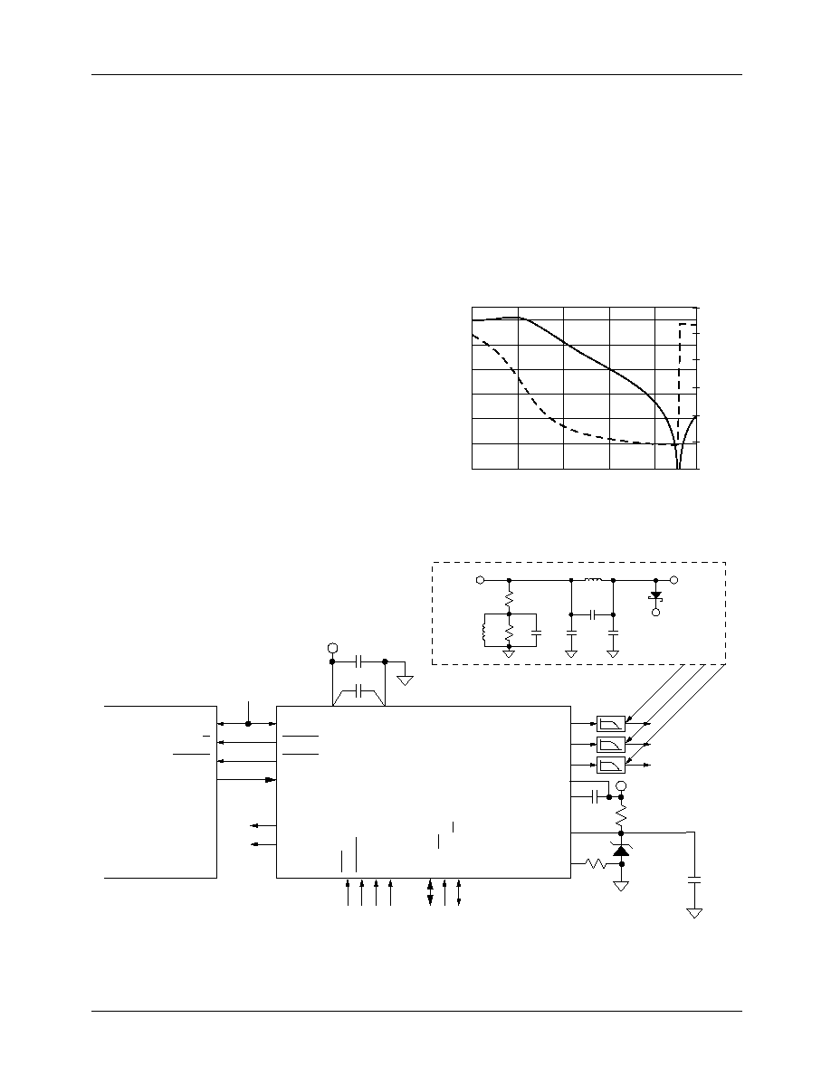
PRODUCT SPECIFICATION
TMC2490A
REV. 1.0.2 2/27/02
31
Applications Information
The circuit in Figure 24 shows the connection of power sup-
ply voltages, output reconstruction filters and the external
voltage reference. All VDD pins should be connected to the
same power source.
The full-scale output voltage level, V
OUT
, on the COMPOS-
ITE, LUMA, and CHROMA pins is found from:
V
OUT
=
I
OUT
x R
L
= K x I
REF
x R
L
= K x (V
REF
/R
REF
) x R
L
where:
· I
OUT
is the full-scale output current sourced by the
TMC2490A D/A converters.
· R
L
is the net resistive load on the COMPOSITE,
CHROMA, and LUMA output pins.
· K is a constant for the TMC2490A D/A converters
(approximately equal to 10.4).
· I
REF
is the reference current flowing out of the R
REF
pin
to ground.
· V
REF
is the voltage measured on the V
REF
pin.
· R
REF
is the total resistance connected between the R
REF
pin and ground.
· A 0.1
µF capacitor should be connected between the C
BYP
pin and the adjacent V
DDA
, pin.
The reference voltage in Figure 24 is from an LM185 1.2
Volt band-gap reference. The 392 Ohm resistor connected
from R
REF
to ground sets the overall "gain" of the three D/A
converters of the TMC2490A. A 787
resistor is used for
single 75
termination. Varying R
REF
±5% will cause the
full-scale output voltage on COMPOSITE, LUMA, and
CHROMA to vary by
±5%.
The suggested output reconstruction filter is the same one
used on the TMC2063P7C Demonstration Board. The phase
and frequency response of this filter is shown in Figure 23.
The Schottky diode is for ESD protection.
Figure 23. Response of Recommended Output Filter
-40
-50
-60
-30
-20
-10
0
-120
-160
-200
-80
-40
0
40
0
5
10
15
20
25
Frequency (MHz)
Analog Reconstruction Filter
Attenuation (dB)
Phase (deg)
24365A
Figure 24. Typical Application Circuit
+5V
+5V
+5V
TMC2490A
Multistandard
Digital Video
Encoder
MPEG-2
Decoder
VDD
GND
PXCK
CHROMA
VIDEO
FROM
ENCODER
VIDEO
OUTPUT
TO 75
LOAD
75
1.0
µH
1.8
µH
27pF
330pF
330pF
1N5818
75
100pF
65-2490(1)A-03
VSYNC
HSYNC
PD
7-0
PIXCLK
B/T
HSYNC
YC
7-0
PDC
SELC
10
µF
LPF
27.0 MHz
CLOCK
CONTROL INTERFACE
VIDEO
INTERFACE
0.1
µF
0.1
µF
0.1
µF
392
3.3k
LM185-1.2
SER
RESET
SA1
SA0/ADR
D
7-0
SCL/CS
SDA / R/W
LUMA
COMPOSITE
C
BYP
V
REF
V
DDA
R
REF

TMC2490A
PRODUCT SPECIFICATION
32
REV. 1.0.2 2/27/02
Notes:

PRODUCT SPECIFICATION
TMC2490A
REV. 1.0.2 2/27/02
33
Notes:

TMC2490A
PRODUCT SPECIFICATION
34
REV. 1.0.2 2/27/02
Notes:
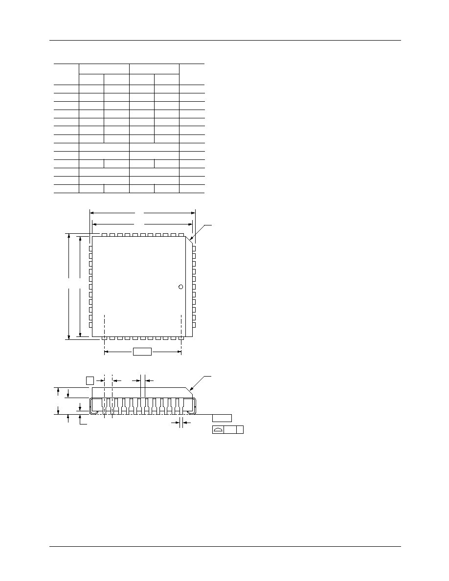
PRODUCT SPECIFICATION
TMC2490A
35
Mechanical Dimensions 44-Pin PLCC Package
D
e
E
A
.165
.180
4.20
4.57
Symbol
Inches
Min.
Max.
Min.
Max.
Millimeters
Notes
E1
J
D1
A
A1
A2
B
B1
D3/E3
J
C
ccc C
LEAD COPLANARITY
A1
.090
.120
2.29
3.04
A2
.020
.51
--
--
B
.013
.021
.33
.53
D/E
.685
.695
17.40
17.65
D1/E1
.650
.656
16.51
16.66
D3/E3
.500 BSC
12.7 BSC
e
.050 BSC
1.27 BSC
J
.042
.056
1.07
1.42
2
3
ND/NE
11
11
N
44
44
ccc
.004
0.10
--
--
B1
.026
.032
.66
.81
Notes:
1.
2.
3.
All dimensions and tolerances conform to ANSI Y14.5M-1982
Corner and edge chamfer (J) = 45
°
Dimension D1 and E1 do not include mold protrusion. Allowable
protrusion is .101" (.25mm)

TMC2490A
PRODUCT SPECIFICATION
2/27/02 0.0m 003
Stock# DS7002490A
1998 Fairchild Semiconductor Corporation
LIFE SUPPORT POLICY
FAIRCHILD'S PRODUCTS ARE NOT AUTHORIZED FOR USE AS CRITICAL COMPONENTS IN LIFE SUPPORT DEVICES
OR SYSTEMS WITHOUT THE EXPRESS WRITTEN APPROVAL OF THE PRESIDENT OF FAIRCHILD SEMICONDUCTOR
CORPORATION. As used herein:
1. Life support devices or systems are devices or systems
which, (a) are intended for surgical implant into the body,
or (b) support or sustain life, and (c) whose failure to
perform when properly used in accordance with
instructions for use provided in the labeling, can be
reasonably expected to result in a significant injury of the
user.
2. A critical component in any component of a life support
device or system whose failure to perform can be
reasonably expected to cause the failure of the life support
device or system, or to affect its safety or effectiveness.
www.fairchildsemi.com
Ordering Information
Product Number
Temperature Range
Screening
Package
Package Marking
TMC2490AR2C
0
°C to 70°C Commercial
44-Lead
PLCC
2490AR2C
DISCLAIMER
FAIRCHILD SEMICONDUCTOR RESERVES THE RIGHT TO MAKE CHANGES WITHOUT FURTHER NOTICE TO
ANY PRODUCTS HEREIN TO IMPROVE RELIABILITY, FUNCTION OR DESIGN. FAIRCHILD DOES NOT ASSUME
ANY LIABILITY ARISING OUT OF THE APPLICATION OR USE OF ANY PRODUCT OR CIRCUIT DESCRIBED HEREIN;
NEITHER DOES IT CONVEY ANY LICENSE UNDER ITS PATENT RIGHTS, NOR THE RIGHTS OF OTHERS.