 | ÐлекÑÑоннÑй компоненÑ: TN6727A | СкаÑаÑÑ:  PDF PDF  ZIP ZIP |
Äîêóìåíòàöèÿ è îïèñàíèÿ www.docs.chipfind.ru
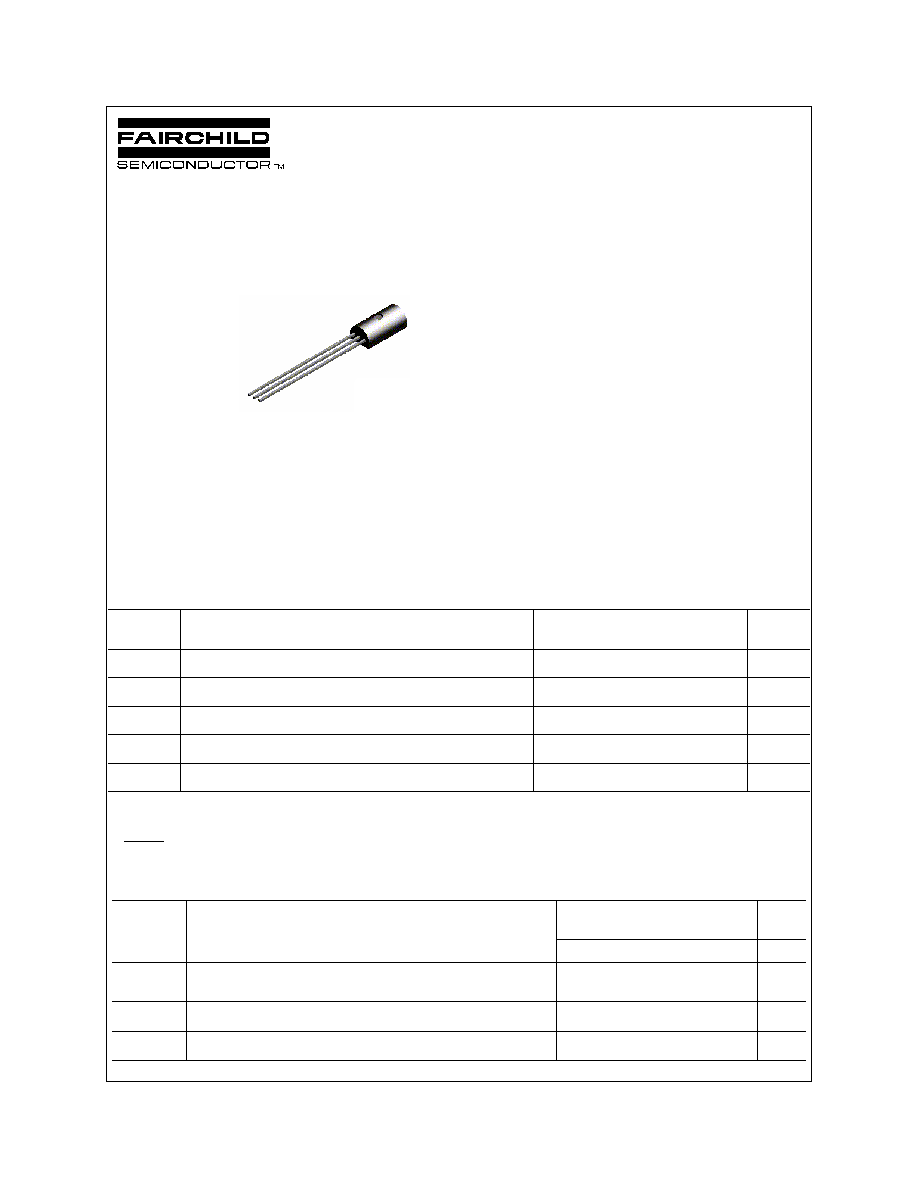
TN6727A
PNP General Purpose Amplifier
This device is designed for general purpose medium power amplifiers and switches requiring collector currents to
1A. Sourced from Process 77. See TN6726A for characteristics.
Absolute Maximum Ratings*
T
A = 25°C unless otherwise noted
°C
-55 to +150
Operating and Storage Junction Temperature Range
T
J,
T
stg
A
1.5
Collector Current - Continuous
I
C
V
5
Emitter-Base Voltage
V
EBO
V
50
Collector-Base Voltage
V
CBO
V
40
Collector-Emitter Voltage
V
CES
Units
Value
Parameter
Symbol
*These ratings are limiting values above which the serviceability of any semiconductor device may be impaired.
NOTES:
1) These ratings are based on a maximum junction temperature of 150°C.
2) These are steady state limits. The factory should be consulted on applications involving pulsed or low duty cycle operations.
Thermal Characteristics
T
A = 25°C unless otherwise noted
°C/W
125
Thermal Resistance, Junction to Ambient
R
JA
°C/W
50
Thermal Resistance, Junction to Case
R
JC
W
mW/°C
1
8
Total Device Dissipation
Derate above 25°C
P
D
TN6727A
Units
Max
Characteristic
Symbol
Page 1 of 2
TN6727A
C
B
E
TO-226
©
1997 Fairchild Semiconductor Corporation
-
25
2.5
I
C
= 50 mA,V
CE
= 10 V, f=20MHz
Small Signal Current Gain
h
fe
pF
30
V
CB
= 10 V, I
E
= 0, f = 1MHz
Output Capacitance
C
cb
SMALL SIGNAL CHARACTERISTICS
V
1.2
I
C
= 1 A, V
CE
= 1 V
Base-Emitter On Voltage
V
BE(on)
V
0.5
I
C
= 1 A, I
B
= 100 mA
Collector-Emitter Saturation Voltage
V
CE(sat)
-
250
55
60
50
I
C
= 10 mA, V
CE
= 1 V
I
C
= 100 mA, V
CE
= 1 V
I
C
= 1A, V
CE
= 1 V
DC Current Gain
h
FE
ON CHARACTERISTICS*
nA
100
V
EB
= 5 V
Emitter Cutoff Current
I
EBO
nA
100
V
CB
= 50 V
Collector Cutoff Current
I
CBO
V
5
I
E
= 1 mA
Emitter-Base Breakdown Voltage
BV
EBO
V
50
I
C
= 1 mA
Collector-Base Breakdown Voltage
BV
CBO
V
40
I
C
= 10 mA
Collector-Emitter Breakdown Voltage
BV
CEO
OFF CHARACTERISTICS
Units
Max
Min
Test Conditions
Parameter
Symbol
PNP General Purpose Amplifier
(continued)
Electrical Characteristics
T
A = 25°C unless otherwise noted
*Pulse Test: Pulse Width
300
µ
s, Duty Cycle
1.0%
Page 2 of 2
TN6727A
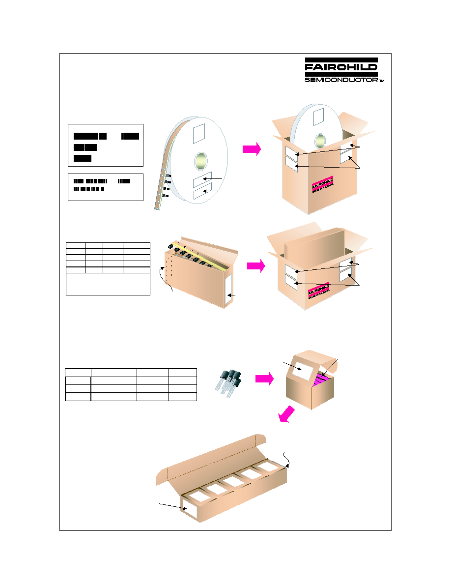
TO-226AE Tape and Reel Data and Package Dimensions
October 1999, Rev. A1
TO -226AE Packaging
Conf iguratio n:
Figur e 1.0
1,500 un its per
EO70 box for
std o pti on
5 EO70 boxes per
Int ermediate B ox
FSCINT Labe l
530mm x 130mm x 83mm
Intermediate box
7,500 un its maximum
per intermedi ate box
for std opt ion
FSCINT Barcode Label
114mm x 102mm x 51mm
EO70 Immediate B ox
Anti -static
Bubble Sheets
(TO-226AE ) BULK PACKING INFORMATION
EOL CODE
DESCRIPTION
LEADCLIP
DIMENSION
QUANTITY
J18Z
TO-18 OPTION STD
NO LEAD CLIP
1.0 K / BOX
J05Z
TO-5 OPTION STD
NO LEAD CLIP
1.0 K / BOX
NO EOL
CODE
TO-226 STANDARD
STRAIGHT
NO LEADCLIP
1.5 K / BOX
TO-226AE TNR/AMMO PACKING INF R
O MATION
Packing
Style
Quantity
EOL code
Reel
A
2,000
D26Z
E
2,000
D27Z
Ammo
M
2,000
D74Z
P
2,000
D75Z
Unit weight = 0.300gm
Reel weight with components = 0.868 kg
Ammo weight with components = 0.880 kg
Max quanti ty per intermediate box = 10,000 units
AMMO PACK OPTION
See Fig 3.0 for 2 Ammo
Pack Options
BULK OPTION
See Bulk Packing
Informat ion table
375mm x 267mm x 375mm
Int ermediate B ox
FSCINT
Labe l
Custom ized
Labe l
333mm x 231mm x 183mm
Int ermediate B ox
FSCINT
Labe l
Custom ized
Labe l
F63TNR
Barcode Label
5 Ammo box es per
Int ermediate B ox
Custom ized
Labe l
327mm x 158mm x 135mm
Immed iate B ox
LOT:
CBVK741B019
NSID:
PN2222N
D/C1:
D9842
SPEC REV:
B2
SPEC:
QTY:
10000
QA REV:
FAIRCHILD SEMICONDUCTOR CORPORATION
HTB:B
(FSCINT)
F63TNR
Labe l
Custom ized
Labe l
5 Reels per
Int ermediate B ox
TAPE and REEL
OPTION
See Fig 2.0 for various
Reeling Styles
F63TNR Label sampl e
FSCINT Label sampl e
Customized
Label
LOT: CBVK741B019
FSID: PN222N
D/C1: D9842 QTY1:
SPEC REV:
SPEC:
QTY: 2000
D/C2:
QTY2:
CPN:
N/F: F (F63TNR)3
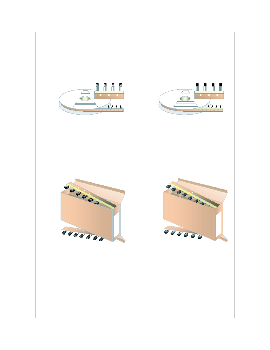
TO-226AE Reeling Style
Configuration:
Figure 2.0
Style "A", D26Z, D70Z (s/h)
Machine Option "A" (H)
Style "E", D27Z, D71Z (s/h)
Machine Option "E" (J)
FIRST WIRE OFF IS EMITTER (ON PKG. 92)
ADHESIVE TAPE IS ON THE TOP SIDE
FLAT OF TRANSISTOR IS ON BOTTOM
FIRST WIRE OFF IS COL LECTOR
ADHESIVE TAPE IS ON BOTTOM SIDE
FLAT OF TRANSISTOR IS ON TOP
ORDER STYLE
D75Z (P)
FIRST WIRE OFF IS COL LECTOR (ON PKG. 92)
ADHESIVE TAPE IS ON THE TOP SIDE
FLAT OF TRANSISTOR IS ON TOP
FIRST WIRE OFF IS EMITTER
ADHESIVE TAPE IS ON BOTTOM SIDE
FLAT OF TRANSISTOR IS ON BOTTOM
ORDER STYLE
D74Z (M)
TO-226AE Radial Ammo Packaging
Configuration: Figure 3.0
TO-226AE Tape and Reel Data and Package Dimensions, continued
October 1999, Rev. A1
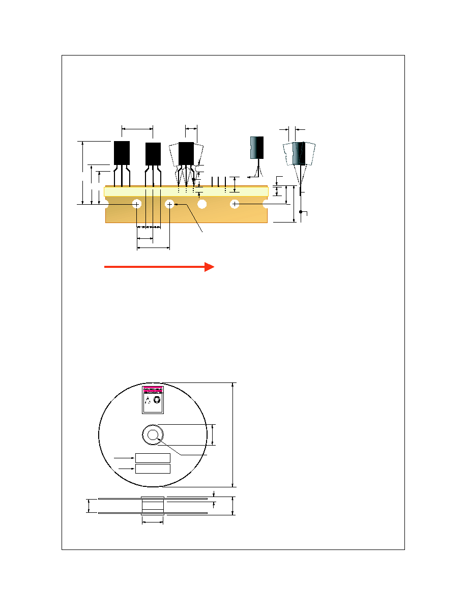
TO-226AE Tape and Reel Data and Package Dimensions, continued
ITEM DESCRIPT ION
Base of Package to Lead Bend
Component Height
Lead Clinch Height
Component B ase Height
Component A lignment ( side/side )
Component A lignment ( front/back )
Component Pitch
Feed Hole Pitch
Hole Center to First Lead
Hole Center to Component Center
Lead Spread
Lead Thickness
Cut Lead Lengt h
Taped Lead Lengt h
Taped Lead Thic kness
Carrier Tape Thickness
Carrier Tape Widt h
Hold - down Tape Width
Hold - down Tape position
Feed Hole Position
Sprocket Hole Diameter
Lead Spring O ut
SYMBOL
b
Hb
HO
H1
Pd
Hd
P
PO
P1
P2
F1/F2
d
L
L1
t
t1
W
WO
W1
W2
DO
S
DIMENSION
0.098 (max)
1.078 (+/- 0.050)
0.630 (+/- 0.020)
0.748 (+/- 0.020)
0.040 (max)
0.031 (max)
0.500 (+/- 0.020)
0.500 (+/- 0.008)
0.150 (+0.009, -0.010)
0.247 (+/- 0.007)
0.104 (+/- 0 .010)
0.018 (+0.002, -0.003)
0.429 (max)
0.209 (+0.051, -0.052)
0.032 (+/- 0.006)
0.021 (+/- 0.006)
0.708 (+0.020, -0.019)
0.236 (+/- 0.012)
0.035 (max)
0.360 (+/- 0.025)
0.157 (+0.008, -0.007)
0.004 (max)
Note : All dimens io ns are in in ches.
Hb
H1 HO
PO
P2
P1 F1
DO
P
Pd
b
d
L1
L
S
WO
W2
W
t
t1
Hd
W1
ITEM DESCRIPTION
SYMBOL
MINIMUM
MAXI MUM
Reel Diame ter
D1
13.975
14.025
Arbor Hole Diameter (Standard)
D2
1.160
1.200
(Small Hole)
D2
0.650
0.700
Core Diameter
D3
3.100
3.300
Hub Recess Inner Diameter
D4
2.700
3.100
Hub Recess Depth
W1
0.370
0.570
Flange to Flange Inner Width
W2
1.630
1.690
Hub to Hub Cent er Widt h
W3
2.090
Note: All dimensions are inches
SEN SI TIVE D EVICES
ELECT ROSTA TIC
D1
D3
W2
W1
W3
D4
D2
TO-226AE Tape and Reel Taping
Dimension Configuration:
Figur e 4.0
TO-226AE Reel
Configuration:
Figur e 5.0
User Direction of Feed
Customized Label
F63TNR Label
October 1999, Rev. A1