 | ÐлекÑÑоннÑй компоненÑ: X55020 | СкаÑаÑÑ:  PDF PDF  ZIP ZIP |
X5328_29_1.1.3.fm
REV 1.1.3 11/13/02
Characteristics subject to change without notice.
1 of 21
www.xicor.com
Replaces X25328/X25329
X5328/X5329
CPU Supervisor with 32Kbit SPI EEPROM
FEATURES
· Low V
CC
detection and reset assertion
--Five standard reset threshold voltages
--Re-program low V
CC
reset threshold voltage
using special programming sequence
--Reset signal valid to V
CC
= 1V
· Long battery life with low power consumption
--<1µA max standby current
--<400µA max active current during read
· 32Kbits of EEPROM
· Built-in inadvertent write protection
--Power-up/power-down protection circuitry
--Protect 0, 1/4, 1/2 or all of EEPROM array with
Block Lock
TM
protection
--In circuit programmable ROM mode
· 2MHz SPI interface modes (0,0 & 1,1)
· Minimize EEPROM programming time
--32-byte page write mode
--Self-timed write cycle
--5ms write cycle time (typical)
· 2.7V to 5.5V and 4.5V to 5.5V power supply
operation
· Available packages
--14-lead TSSOP, 8-lead SOIC
DESCRIPTION
These devices combine three popular functions, Power-
on Reset Control, Supply Voltage Supervision, and
Block Lock Protect Serial EEPROM Memory in one
package. This combination lowers system cost, reduces
board space requirements, and increases reliability.
Applying power to the device activates the power on
reset circuit which holds RESET/RESET active for a
period of time. This allows the power supply and oscilla-
tor to stabilize before the processor can execute code.
The device's low V
CC
detection circuitry protects the
user's system from low voltage conditions by holding
RESET/RESET active when V
CC
falls below a mini-
mum V
CC
trip point. RESET/RESET remains asserted
until V
CC
returns to proper operating level and stabi-
lizes. Five industry standard V
TRIP
thresholds are
available, however, Xicor's unique circuits allow the
threshold to be reprogrammed to meet custom
requirements or to fine-tune the threshold in applica-
tions requiring higher precision.
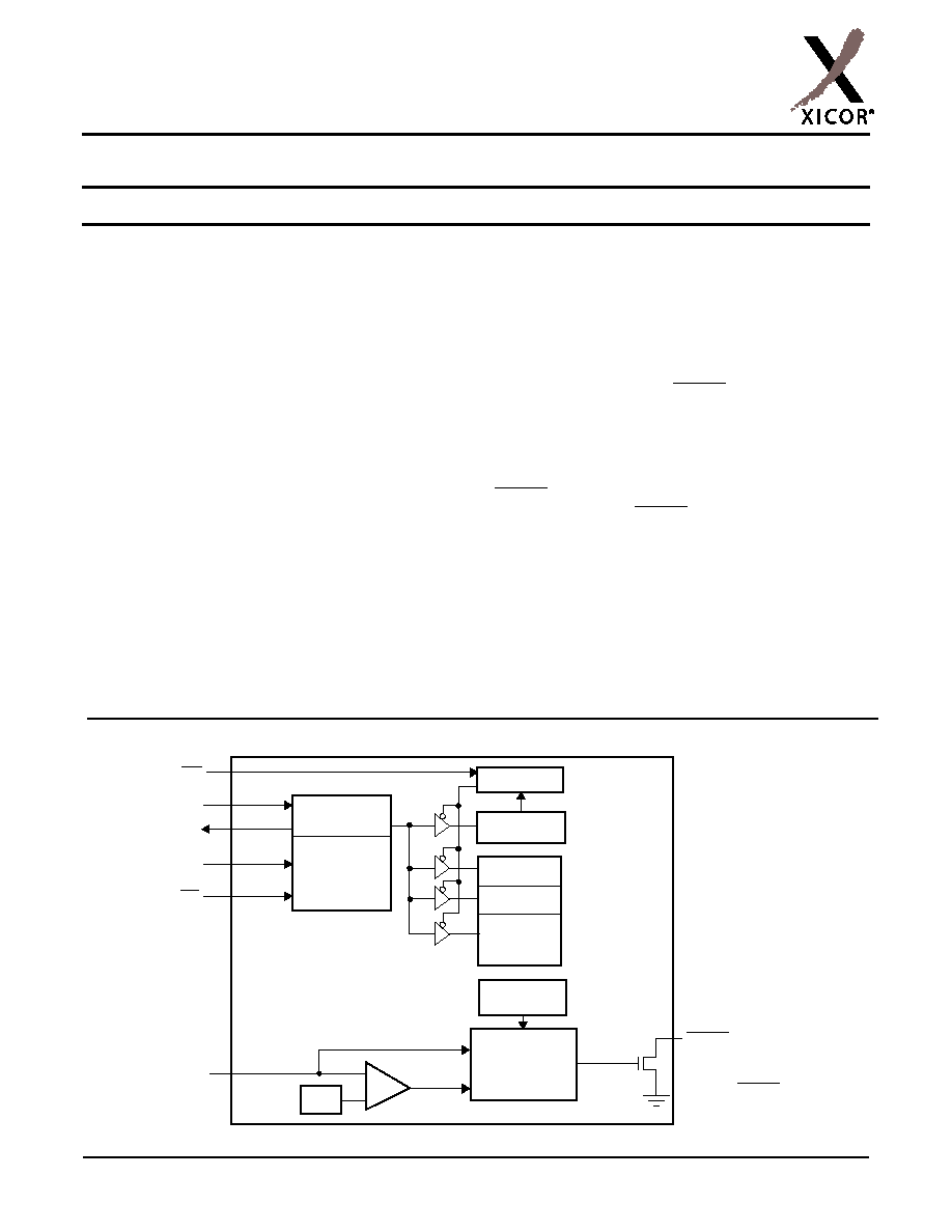
BLOCK DIAGRAM
Data
Register
Command
Decode &
Control
Logic
SI
SO
SCK
CS
V
CC
Reset
Timebase
Power on and
Generation
V
TRIP
+
-
RESET/RESET
Reset
Low Voltage
Status
Register
Protect Logic
8Kbits
8Kbits
16Kbits
EEPROM Array
WP
X5328 = RESET
X5329 = RESET
X5328/X5329
Characteristics subject to change without notice.
2 of 21
REV 1.1.3 11/13/02
www.xicor.com
PIN DESCRIPTION
PIN CONFIGURATION
Pin
(SOIC/PDIP)
Pin
TSSOP
Name
Function
1
1
CS
Chip Select Input.
CS HIGH, deselects the device and the SO output pin is at
a high impedance state. Unless a nonvolatile write cycle is underway, the device
will be in the standby power mode. CS LOW enables the device, placing it in the
active power mode. Prior to the start of any operation after power up, a HIGH to
LOW transition on CS is required.
2
2
SO
Serial Output.
SO is a push/pull serial data output pin. A read cycle shifts data out
on this pin. The falling edge of the serial clock (SCK) clocks the data out.
5
8
SI
Serial Input.
SI is a serial data input pin. Input all opcodes, byte addresses, and
memory data on this pin. The rising edge of the serial clock (SCK) latches the input
data. Send all opcodes (Table 1), addresses and data MSB first.
6
9
SCK
Serial Clock.
The Serial Clock controls the serial bus timing for data input and out-
put. The rising edge of SCK latches in the opcode, address, or data bits present on
the SI pin. The falling edge of SCK changes the data output on the SO pin.
3
6
WP
Write Protect.
The WP pin works in conjunction with a nonvolatile WPEN bit to
"lock" the setting of the Watchdog Timer control and the memory write protect bits.
4
7
V
SS
Ground
8
14
V
CC
Supply Voltage
7
13
RESET/
RESET
Reset Output
. RESET/RESET is an active LOW/HIGH, open drain output
which goes active whenever V
CC
falls below the minimum V
CC
sense level. It
will remain active until V
CC
rises above the minimum V
CC
sense level for 200ms.
RESET/RESET goes active on power up at about 1V and remains active for
200ms after the power supply stabilizes.
3-5,10-12
NC
No internal connections
8-Lead SOIC/PDIP
CS
WP
SO
1
2
3
4
RESET/RESET
8
7
6
5
14-Lead TSSOP
SO
WP
V
SS
1
2
3
4
5
6
7
RESET/RESET
SCK
SI
14
13
12
11
10
9
8
NC
V
CC
NC
X5328/29
V
CC
SCK
SI
CS
NC
NC
NC
NC
X5328/29
V
CC

X5328/X5329
Characteristics subject to change without notice.
3 of 21
REV 1.1.3 11/13/02
www.xicor.com
PRINCIPLES OF OPERATION
Power On Reset
Application of power to the X5328/X5329 activates a
Power On Reset Circuit. This circuit goes active at
about 1V and pulls the RESET/RESET pin active. This
signal prevents the system microprocessor from start-
ing to operate with insufficient voltage or prior to stabili-
zation of the oscillator. When V
CC
exceeds the device
V
TRIP
value for 200ms (nominal) the circuit releases
RESET/RESET, allowing the processor to begin exe-
cuting code.
Low Voltage Monitoring
During operation, the X5328/X5329 monitors the V
CC
level and asserts RESET/RESET if supply voltage falls
below a preset minimum V
TRIP
. The RESET/RESET
signal prevents the microprocessor from operating in a
power fail or brownout condition. The RESET/RESET
signal remains active until the voltage drops below 1V.
It also remains active until V
CC
returns and exceeds
V
TRIP
for 200ms.
V
CC
Threshold Reset Procedure
The X5328/X5329 has a standard V
CC
threshold
(V
TRIP
) voltage. This value will not change over normal
operating and storage conditions. However, in applica-
tions where the standard V
TRIP
is not exactly right, or
for higher precision in the V
TRIP
value, the X5328/
X5329 threshold may be adjusted.
Setting the V
TRIP
Voltage
This procedure sets the V
TRIP
to a higher voltage
value. For example, if the current V
TRIP
is 4.4V and the
new V
TRIP
is 4.6V, this procedure directly makes the
change. If the new setting is lower than the current set-
ting, then it is necessary to reset the trip point before
setting the new value.
To set the new V
TRIP
voltage, apply the desired V
TRIP
threshold to the V
CC
pin and tie the CS pin and the WP
pin HIGH. RESET/RESET and SO pins are left uncon-
nected. Then apply the programming voltage V
P
to
both SCK and SI and pulse CS LOW then HIGH.
Remove V
P
and the sequence is complete.
Figure 1. Set V
TRIP
Voltage
Resetting the V
TRIP
Voltage
This procedure sets the V
TRIP
to a "native" voltage
level. For example, if the current V
TRIP
is 4.4V and the
V
TRIP
is reset, the new V
TRIP
is something less than
1.7V. This procedure must be used to set the voltage to
a lower value.
To reset the V
TRIP
voltage, apply a voltage between 2.7
and 5.5V to the V
CC
pin. Tie the CS pin, the WP pin,
and the SCK pin HIGH. RESET/RESET and SO pins
are left unconnected. Then apply the programming volt-
age V
P
to the SI pin ONLY and pulse CS LOW then
HIGH. Remove V
P
and the sequence is complete.
Figure 2. Reset V
TRIP
Voltage
SCK
SI
V
P
V
P
CS
SCK
SI
V
CC
V
P
CS
X5328/X5329
Characteristics subject to change without notice.
4 of 21
REV 1.1.3 11/13/02
www.xicor.com
Figure 3. V
TRIP
Programming Sequence Flow Chart
V
TRIP
Programming
Apply 5V to V
CC
Decrement V
CC
RESET pin
goes active?
Measured V
TRIP
-
Desired V
TRIP
DONE
Execute
Sequence
Reset V
TRIP
Set V
CC
= V
CC
Applied =
Desired V
TRIP
Execute
Sequence
Set V
TRIP
New V
CC
Applied =
Old V
CC
Applied + Error
(V
CC
= V
CC
- 10mV)
Execute
Sequence
Reset V
TRIP
New V
CC
Applied =
Old V
CC
Applied - Error
Error
Emax
Error < Emax
YES
NO
Error > Emax
Emax = Maximum Desired Error
Figure 4. Sample V
TRIP
Reset Circuit
1
2
3
4
8
7
6
5
X5328/29
V
TRIP
Adj.
Program
NC
NC
V
P
Reset
V
TRIP
Test
V
TRIP
Set
V
TRIP
NC
RESET
4.7K
4.7K
10K
10K
+

X5328/X5329
Characteristics subject to change without notice.
5 of 21
REV 1.1.3 11/13/02
www.xicor.com
SPI SERIAL MEMORY
The memory portion of the device is a CMOS Serial
EEPROM array with Xicor's block lock protection. The
array is internally organized as x 8. The device features
a Serial Peripheral Interface (SPI) and software proto-
col allowing operation on a simple four-wire bus.
The device utilizes Xicor's proprietary Direct Write
TM
cell, providing a minimum endurance of 100,000 cycles
and a minimum data retention of 100 years.
The device is designed to interface directly with the
synchronous Serial Peripheral Interface (SPI) of many
popular microcontroller families. It contains an 8-bit
instruction register that is accessed via the SI input,
with data being clocked in on the rising edge of SCK.
CS must be LOW during the entire operation.
All instructions (Table 1), addresses and data are trans-
ferred MSB first. Data input on the SI line is latched on
the first rising edge of SCK after CS goes LOW. Data is
output on the SO line by the falling edge of SCK. SCK
is static, allowing the user to stop the clock and then
start it again to resume operations where left off.
Write Enable Latch
The device contains a Write Enable Latch. This latch
must be SET before a Write Operation is initiated. The
WREN instruction will set the latch and the WRDI
instruction will reset the latch (Figure 3). This latch is
automatically reset upon a power-up condition and
after the completion of a valid Write Cycle.
Status Register
The RDSR instruction provides access to the Status
Register. The Status Register may be read at any time,
even during a Write Cycle. The Status Register is for-
matted as follows:
*Bits (5,4) should be written as `1' only.
The Write-In-Progress (WIP) bit is a volatile, read only
bit and indicates whether the device is busy with an
internal nonvolatile write operation. The WIP bit is read
using the RDSR instruction. When set to a "1", a non-
volatile write operation is in progress. When set to a "0",
no write is in progress.
7
6
5
4
3
2
1
0
WPEN
FLB
1*
1*
BL1
BL0
WEL
WIP
Table 1. Instruction Set
Note:
*Instructions are shown MSB in leftmost position. Instructions are transferred MSB first.
Table 2. Block Protect Matrix
Instruction Name
Instruction Format*
Operation
WREN
0000 0110
Set the Write Enable Latch (Enable Write Operations)
SFLB
0000 0000
Set Flag Bit
WRDI/RFLB
0000 0100
Reset the Write Enable Latch/Reset Flag Bit
RSDR
0000 0101
Read Status Register
WRSR
0000 0001
Write Status Register (Block Lock, WPEN & Flag Bits)
READ
0000 0011
Read Data from Memory Array Beginning at Selected Address
WRITE
0000 0010
Write Data to Memory Array Beginning at Selected Address
WREN CMD
Status Register
Device Pin
Block
Block
Status Register
WEL
WPEN
WP#
Protected Block
Unprotected Block
WPEN, BL0, BL1,
WD0, WD1
0
X
X
Protected
Protected
Protected
1
1
0
Protected
Writable
Protected
1
0
X
Protected
Writable
Writable
1
X
1
Protected
Writable
Writable