 | ÐлекÑÑоннÑй компоненÑ: X9410Y | СкаÑаÑÑ:  PDF PDF  ZIP ZIP |
/home/web/doc/html/fairchild/206646
REV 1.1 10/6/00
Characteristics subject to change without notice.
1 of 21
www.xicor.com
Low Noise/Low Power/SPI Bus
X9410
Dual Digitally Controlled Potentiometer (XDCP
TM
)
FEATURES
· Two potentiometers in one package
· SPI serial interface
· Register oriented format
--Direct read/write/transfer wiper positions
--Store as many as four positions per
potentiometer
· Power supplies
--V
CC
= 2.7V to 5.5V
--V+ = 2.7V to 5.5V
--V = 2.7V to 5.5V
· Low power CMOS
--Standby current < 1µA
· High reliability
--Endurance100,000 data changes per bit per
register
--Register data retention100 years
· 8-bytes of nonvolatile EEPROM memory
· 10K
resistor arrays
· Resolution: 64 taps each pot
· 24-lead TSSOP, 24-lead SOIC and 24-pin plastic
DIP packages
DESCRIPTION
The X9410 integrates two digitally controlled
potentiometers (XDCP) on a monolithic CMOS
integrated microcircuit.
The digitally controlled potentiometer is implemented
using 63 resistive elements in a series array. Between
each element are tap points connected to the wiper
terminal through switches. The position of the wiper on
the array is controlled by the user through the SPI bus
interface. Each potentiometer has associated with it a
volatile Wiper Counter Register (WCR) and 4
nonvolatile Data Registers (DR0:DR3) that can be
directly written to and read by the user. The contents
of the WCR controls the position of the wiper on the
resistor array through the switches. Power up recalls
the contents of DR0 to the WCR.
The XDCP can be used as a three-terminal
potentiometer or as a two-terminal variable resistor in
a wide variety of applications including control,
parameter adjustments, and signal processing.
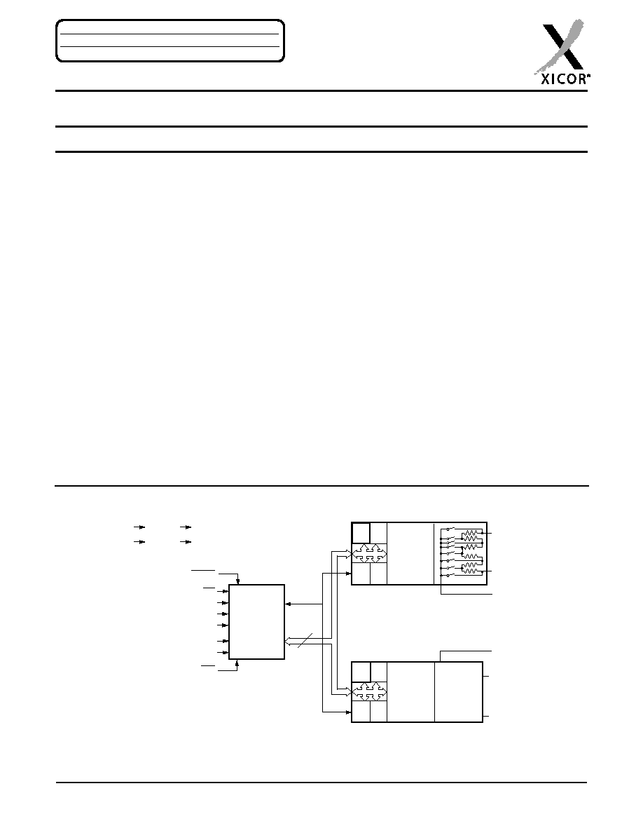
BLOCK DIAGRAM
R0 R1
R2 R3
Wiper
Counter
Register
(WCR)
Resistor
Array
Pot1
V
H1
/R
H1
V
L1
/R
L1
R0 R1
R2 R3
Wiper
Counter
Register
(WCR)
Interface
and
Control
Circuitry
CS
SCK
A0
A1
V
H0
/R
H0
V
L0
/R
L0
Data
8
V
W0
/R
W0
V
W1
/R
W1
SO
SI
HOLD
WP
Pot 0
V
CC
V
SS
V+
V-
Pot 1
A
PPLICATION
N
OTES
A V A I L A B L E
AN99 · AN115 · AN120 · AN124 · AN133 · AN134 · AN135
X9410
Characteristics subject to change without notice.
2 of 21
REV 1.1 10/6/00
www.xicor.com
PIN DESCRIPTIONS
Host Interface Pins
Serial Output (SO)
SO is a push/pull serial data output pin. During a read
cycle, data is shifted out on this pin. Data is clocked out
by the falling edge of the serial clock.
Serial Input
SI is the serial data input pin. All opcodes, byte
addresses and data to be written to the pots and pot
registers are input on this pin. Data is latched by the
rising edge of the serial clock.
Serial Clock (SCK)
The SCK input is used to clock data into and out of the
X9410.
Chip Select (CS)
When CS is HIGH, the X9410 is deselected and the
SO pin is at high impedance, and (unless an internal
write cycle is underway) the device will be in the
standby state. CS LOW enables the X9410, placing it in
the active power mode. It should be noted that after a
power-up, a HIGH to LOW transition on CS is required
prior to the start of any operation.
Hold (HOLD)
HOLD is used in conjunction with the CS pin to select
the device. Once the part is selected and a serial
sequence is underway, HOLD may be used to pause
the serial communication with the controller without
resetting the serial sequence. To pause, HOLD must be
brought LOW while SCK is LOW. To resume
communication, HOLD is brought HIGH, again while
SCK is LOW. If the pause feature is not used, HOLD
should be held HIGH at all times.
Device Address (A
0
A
1
)
The address inputs are used to set the least significant
2 bits of the 8-bit slave address. A match in the slave
address serial data stream must be made with the
address input in order to initiate communication with
the X9410. A maximum of 4 devices may occupy the
SPI serial bus.
Potentiometer Pins
V
H
/R
H
(V
H0
/R
H0
--V
H1
/R
H1
), V
L
/R
L
(V
L0
/R
L0
--V
L1
/R
L1
)
The V
H
/R
H
and V
L
/R
L
inputs are equivalent to the terminal
connections on either end of a mechanical potentiometer.
V
W
/R
W
(V
W0
/R
W0
--V
W1
/R
W1
)
The wiper outputs are equivalent to the wiper output of
a mechanical potentiometer.
Hardware Write Protect Input (WP)
The WP pin when LOW prevents nonvolatile writes to
the Data Registers.
Analog Supplies (V+, V-)
The analog supplies V+, V- are the supply voltages for
the XDCP analog section.
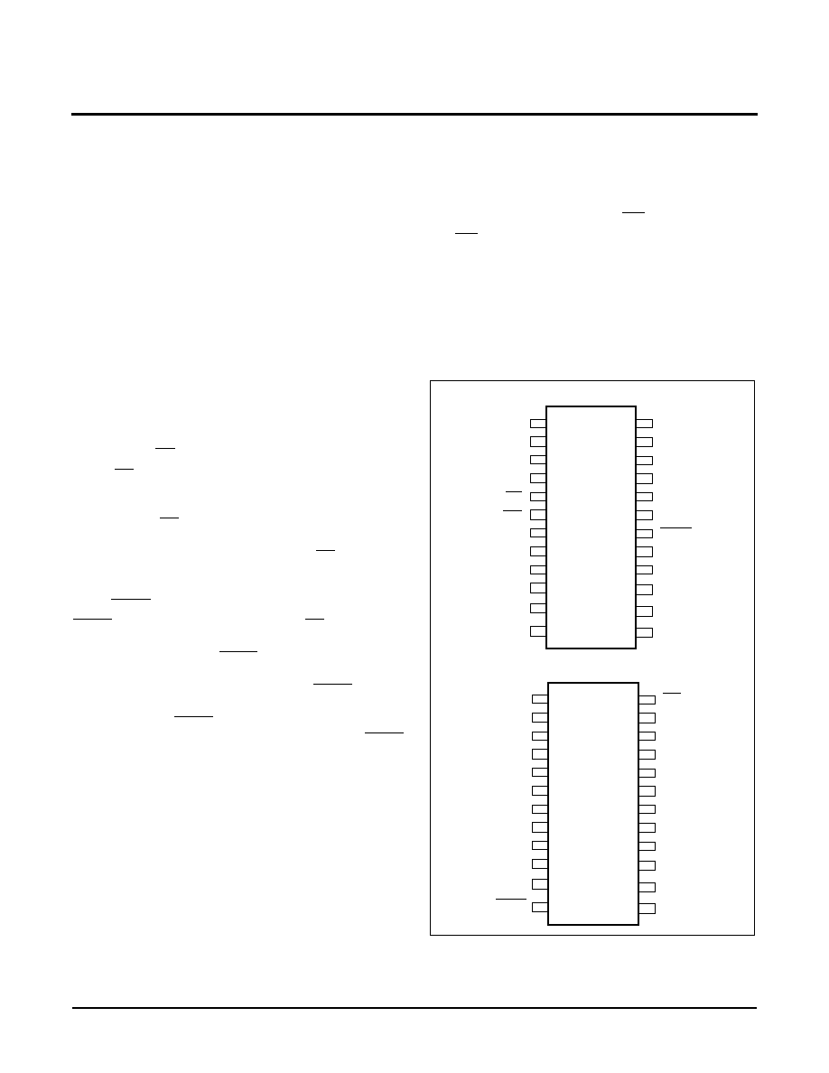
PIN CONFIGURATION
V
CC
V
L0
/R
L0
V
H0
/R
H0
WP
SI
A
1
1
2
3
4
5
6
7
8
9
10
24
23
22
21
20
19
18
17
16
15
V+
A
0
SO
HOLD
SCK
DIP/SOIC
X9410
V
SS
V
W0
/R
W0
14
13
11
12
CS
V
L1
/R
L1
V
H1
/R
H1
V
W1
/R
W1
V-
SI
A
1
V
L1
/R
L1
1
2
3
4
5
6
7
8
9
10
24
23
22
21
20
19
18
17
16
15
WP
CS
V
W0
/R
W0
V
H0
/R
H0
V
L0
/R
L0
V
CC
TSSOP
X9410
HOLD
V
H1
/R
H1
14
13
11
12
V
W1
/R
W1
SCK
A
0
SO
V
SS
NC
NC
NC
NC
NC
NC
NC
NC
NC
V+
V-
NC
NC
NC
X9410
Characteristics subject to change without notice.
3 of 21
REV 1.1 10/6/00
www.xicor.com
PIN NAMES
DEVICE DESCRIPTION
The X9410 is a highly integrated microcircuit
incorporating two resistor arrays and their associated
registers and counters and the serial interface logic
providing direct communication between the host and
the XDCP potentiometers.
Serial Interface
The X9410 supports the SPI interface hardware
conventions. The device is accessed via the SI input
with data clocked in on the rising SCK. CS must be
LOW and the HOLD and WP pins must be HIGH during
the entire operation.
The SO and SI pins can be connected together, since
they have three state outputs. This can help to reduce
system pin count.
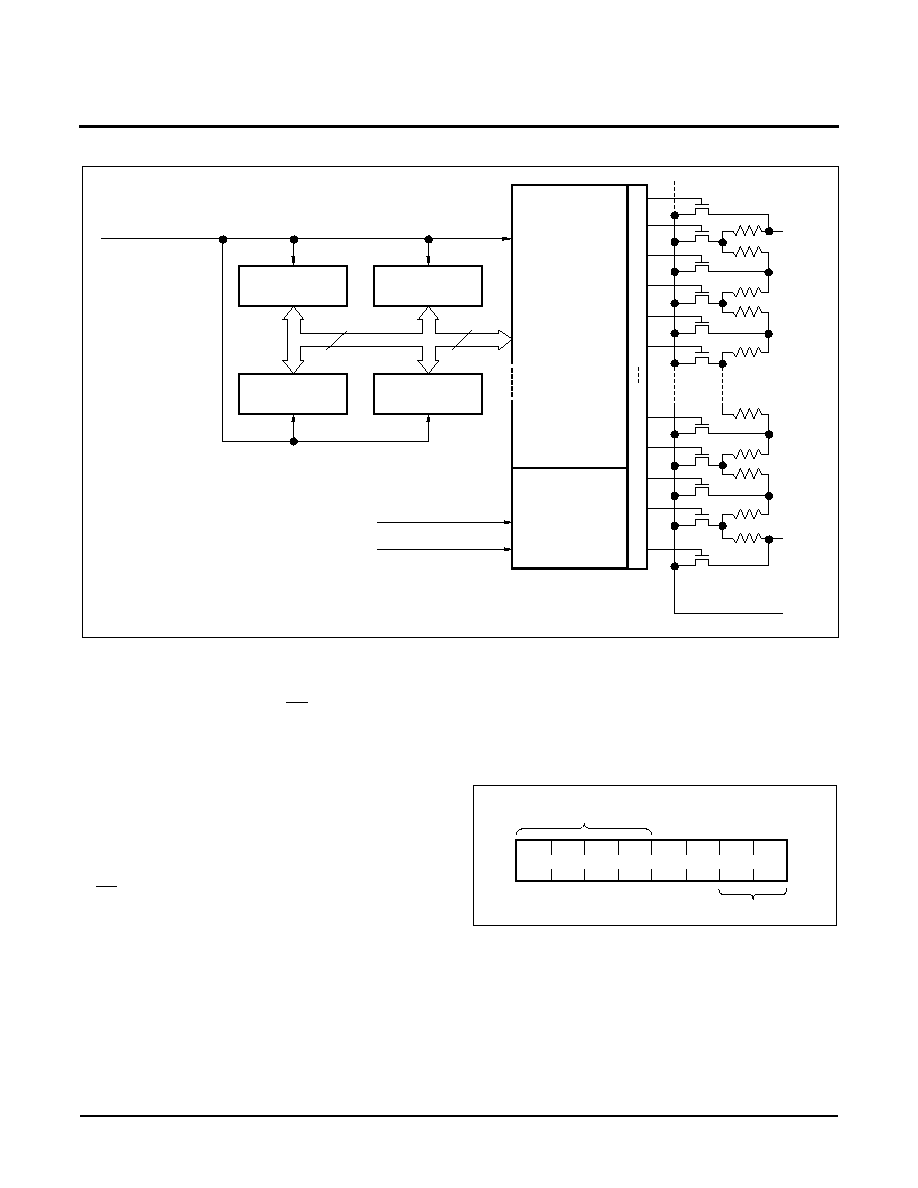
Array Description
The X9410 is comprised of two resistor arrays. Each
array contains 63 discrete resistive segments that are
connected in series. The physical ends of each array
are equivalent to the fixed terminals of a mechanical
potentiometer (V
H
/R
H
and V
L
/R
L
inputs).
At both ends of each array and between each resistor
segment is a CMOS switch connected to the wiper
(V
W
/R
W
) output. Within each individual array only one
switch may be turned on at a time.
These switches are controlled by a Wiper Counter
Register (WCR). The six bits of the WCR are decoded
to select, and enable, one of sixty-four switches.
Wiper Counter Register (WCR)
The X9410 contains two Wiper Counter Registers, one
for each XDCP potentiometer. The WCR is equivalent
to a serial-in, parallel-out register/counter with its
outputs decoded to select one of sixty-four switches
along its resistor array. The contents of the WCR can
be altered in four ways: it may be written directly by the
host via the Write Wiper Counter Register instruction
(serial load); it may be written indirectly by transferring
the contents of one of four associated Data Registers
via the XFR Data Register or Global XFR Data
Register instructions (parallel load); it can be modified
one step at a time by the Increment/ Decrement
instruction. Finally, it is loaded with the contents of its
Data Register zero (DR0) upon power-up.
The Wiper Counter Register is a volatile register; that
is, its contents are lost when the X9410 is powered-
down. Although the register is automatically loaded
with the value in DR0 upon power-up, this may be
different from the value present at power-down.
Data Registers
Each potentiometer has four 6-bit nonvolatile Data
Registers. These can be read or written directly by the
host. Data can also be transferred between any of the
four Data Registers and the associated Wiper Counter
Register. All operations changing data in one of the
Data Registers is a nonvolatile operation and will take a
maximum of 10ms.
If the application does not require storage of multiple
settings for the potentiometer, the Data Registers can
be used as regular memory locations for system
parameters or user preference data.
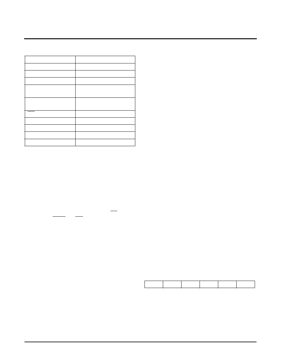
Data Register Detail
Symbol
Description
SCK
Serial Clock
S
I
, S
O
Serial Data
A
0
-A
1
Device Address
V
H0
/R
H0
V
H1
/R
H1
,
V
L0
/R
L0
V
L1
/R
L1
Potentiometer Pins
(terminal equivalent)
V
W0
/R
W0
V
W1
/R
W1
Potentiometer Pin
(wiper equivalent)
WP
Hardware Write Protection
V+,V-
Analog Supplies
V
CC
System Supply Voltage
V
SS
System Ground
NC
No Connection
(MSB)
(LSB)
D5
D4
D3
D2
D1
D0
NV
NV
NV
NV
NV
NV
X9410
Characteristics subject to change without notice.
4 of 21
REV 1.1 10/6/00
www.xicor.com
Write in Process
The contents of the Data Registers are saved to
nonvolatile memory when the CS pin goes from LOW
to HIGH after a complete write sequence is received by
the device. The progress of this internal write operation
can be monitored by a Write In Process bit (WIP). The
WIP bit is read with a Read Status command.
INSTRUCTIONS
Identification (ID) Byte
The first byte sent to the X9410 from the host, following
a CS going HIGH to LOW, is called the Identification
byte. The most significant four bits of the slave address
are a device type identifier, for the X9410 this is fixed
as 0101[B] (refer to Figure 2).
The two least significant bits in the ID byte select one of
four devices on the bus. The physical device address is
defined by the state of the A
0
-A
1
input pins. The X9410
compares the serial data stream with the address input
state; a successful compare of both address bits is
required for the X9410 to successfully continue the
command sequence. The A
0
A
1
inputs can be actively
driven by CMOS input signals or tied to V
CC
or V
SS
.
The remaining two bits in the ID byte must be set to 0.
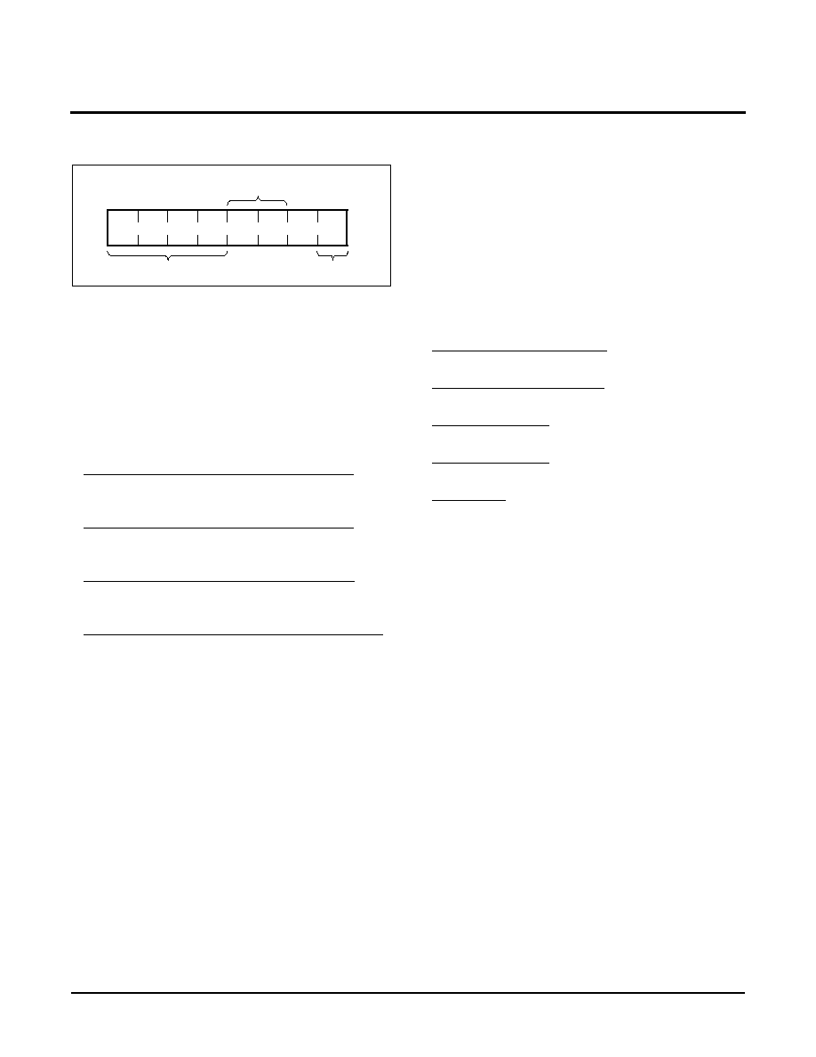
Figure 2. Identification Byte Format
Instruction Byte
The next byte sent to the X9410 contains the
instruction and register pointer information. The four
most significant bits are the instruction. The next four
bits point to one of the two pots and when applicable
they point to one of four associated registers. The
format is shown below in Figure 3.
1
0
0
0
0
A1
A0
Device Type
Identifier
Device Address
1
Figure 1. Detailed Potentiometer Block Diagram
Serial Data Path
From Interface
Circuitry
Register 0
Register 1
Register 2
Register 3
Serial
Bus
Input
Parallel
Bus
Input
Wiper
Counter
Register
INC/DEC
Logic
UP/DN
CLK
Modified SCL
UP/DN
V
H
/R
H
V
L
/R
L
V
W
/R
W
If WCR = 00[H] then V
W
/R
W
= V
L
/R
L
If WCR = 3F[H] then V
W
/R
W
= V
H
/R
H
8
6
C
o
u
n
t
e
r
D
e
c
o
d
e
(WCR)
(One of Two Arrays)
X9410
Characteristics subject to change without notice.
5 of 21
REV 1.1 10/6/00
www.xicor.com
Figure 3. Instruction Byte Format
The four high order bits of the instruction byte specify
the operation. The next two bits (R
1
and R
0
) select one
of the four registers that is to be acted upon when a
register oriented instruction is issued. The last bit (P
0
)
selects which one of the two potentiometers is to be
affected by the instruction.
Four of the ten instructions are two bytes in length and
end with the transmission of the instruction byte. These
instructions are:
XFR Data Register to Wiper Counter Register--This
transfers the contents of one specified Data Register
to the associated Wiper Counter Register.
XFR Wiper Counter Register to Data Register--This
transfers the contents of the specified Wiper Counter
Register to the specified associated Data Register.
Global XFR Data Register to Counter Register--This
transfers the contents of both specified Data Registers
to the associated Wiper Counter Registers.
Global XFR Wiper Counter Register to Data Register--
This transfers the contents of both Wiper Counter
Registers to the specified associated Data Registers.
The basic sequence of the two byte instructions is
illustrated in Figure 4. These two-byte instructions
exchange data between the WCR and one of the data
registers. A transfer from a Data Register to a WCR is
essentially a write to a static RAM, with the static RAM
controlling the wiper position. The response of the
wiper to this action will be delayed by t
WRL
. A transfer
from the WCR (current wiper position), to a data register
is a write to nonvolatile memory and takes a minimum
of t
WR
to complete. The transfer can occur between
one of the two potentiometers and one of its associated
registers; or it may occur globally, where the transfer
occurs between both potentiometers and one
associated register.
Five instructions require a three-byte sequence to
complete. These instructions transfer data between the
host and the X9410; either between the host and one
of the data registers or directly between the host and
the Wiper Counter Register. These instructions are:
Read Wiper Counter Register--read the current
wiper position of the selected pot,
Write Wiper Counter Register--change current wiper
position of the selected pot,
Read Data Register--read the contents of the
selected data register;
Write Data Register--write a new value to the
selected data register.
Read Status--This command returns the contents of
the WIP bit which indicates if the internal write cycle
is in progress.
The sequence of these operations is shown in Figure 5
and Figure 6.
The final command is Increment/Decrement. It is
different from the other commands because it's length
is indeterminate. Once the command is issued, the
master can clock the selected wiper up and/or down in
one resistor segment steps, thereby providing a fine
tuning capability to the host. For each SCK clock pulse
(t
HIGH
) while SI is HIGH, the selected wiper will move
one resistor segment towards the V
H
/R
H
terminal.
Similarly, for each SCK clock pulse while SI is LOW, the
selected wiper will move one resistor segment towards
the V
L
/R
L
terminal. A detailed illustration of the
sequence and timing for this operation are shown in
Figures 7-8.
I1
I2
I3
I0
R1
R0
0
P0
Pot Select
Register
Select
Instructions