Äîêóìåíòàöèÿ è îïèñàíèÿ www.docs.chipfind.ru
Preliminary Data Sheet
2.2
1
Preliminary specifications subject to change without notice
Filtronic Compound Semiconductors Ltd
Contact Details (UK): Tel: +44 (0) 1325 301111 Fax: +44 (0) 1325 306177 Email: sales@filcs.com
Contact Details (USA): Tel: +1 (408) 850 5790 Fax: +1 (408) 850 5766 Email: sales@filcsi.com
Website: www.filcs.com
FMS2017
2.4GHz DPDT GaAs Single-Band WLAN Switch
Features:
Available as RF known good die
Suitable for Single-band WLAN 802.11b/g
Applications
Excellent low control voltage performance
Very low Insertion loss typ. 0.55dB at 2.4GHz
High isolation typ. 23dB at 2.4GHz
Description and Applications:
The FMS2017 is a low loss, single band Gallium Arsenide antenna diversity switch designed for use
in Wireless LAN applications. The die is fabricated using the Filtronic FL05 0.5
µm switch process
technology that offers leading edge performance, optimised for switch applications. The FMS2017 is
designed for use in 802.11b/g WLAN modules.
Electrical Specifications:
(T
AMBIENT
= 25°C,V
ctrl
= 0V/(2.4V,+3.3V), Z
IN
= Z
OUT
= 50
)
Parameter
Conditions
Min
Typ
Max
Units
Insertion Loss (All Paths)
2.5GHz, Small Signal
0.55
dB
Isolation (All Paths)
2.5GHz, Small Signal
23
dB
Return Loss
2.5GHz, Small Signal
20
dB
P1dB
2.5GHz Control Voltage 3.0V
37
dBm
2nd Harmonic Level
2.4GHz, Pin = 32dBm, Vctrl =2.4V
-65
dBc
3rd Harmonic Level
2.4GHz, Pin = 32dBm, Vctrl =2.4V
-65
dBc
Switching speed
Vctrl=2.4V, Pin=20dBm
20
nS
Note: External DC blocking capacitors are required on all RF ports (typ: 47pF)
All unused ports terminated in 50
.
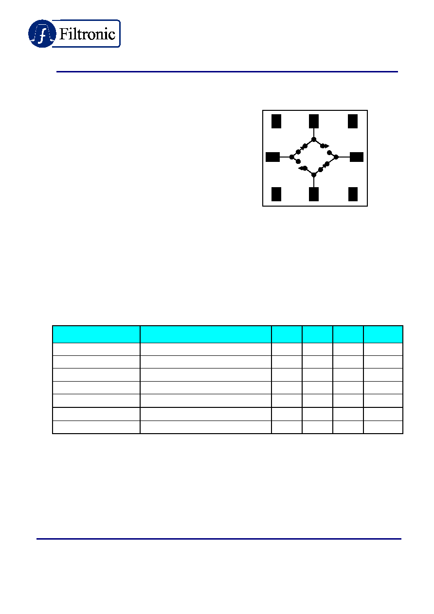
Functional Schematic
V4
TX
V3
AN1
ANT2
V1
RX V2
Preliminary Data Sheet
2.2
2
Preliminary specifications subject to change without notice
Filtronic Compound Semiconductors Ltd
Contact Details (UK): Tel: +44 (0) 1325 301111 Fax: +44 (0) 1325 306177 Email: sales@filcs.com
Contact Details (USA): Tel: +1 (408) 850 5790 Fax: +1 (408) 850 5766 Email: sales@filcsi.com
Website: www.filcs.com
FMS2017
Absolute Maximum Ratings:
Parameter
Symbol
Absolute Maximum
Max Input Power
Pin
+36dBm
Control Voltage
Vctrl
+5V
Operating Temperature
Toper
-40°C to +100°C
Storage Temperature
Tstor
-55°C to +150°C
Note: Exceeding any one of these absolute maximum ratings may cause permanent damage to the
device.
Truth Table:
State
V1
V2
V3
V4
PATH(S)
1 High Low Low Low
RX-ANT1
2 Low
High Low Low
RX-ANT2
3 Low Low High
Low
TX-ANT2
4 Low Low Low
High
TX-ANT1
5
Low
High
Low
High
TX-ANT1 & RX-ANT2
6 High Low High Low TX-ANT2
&
RX-ANT1
Note:
`High' = +2.4V to +3.3V
`Low' = 0V to +0.2V
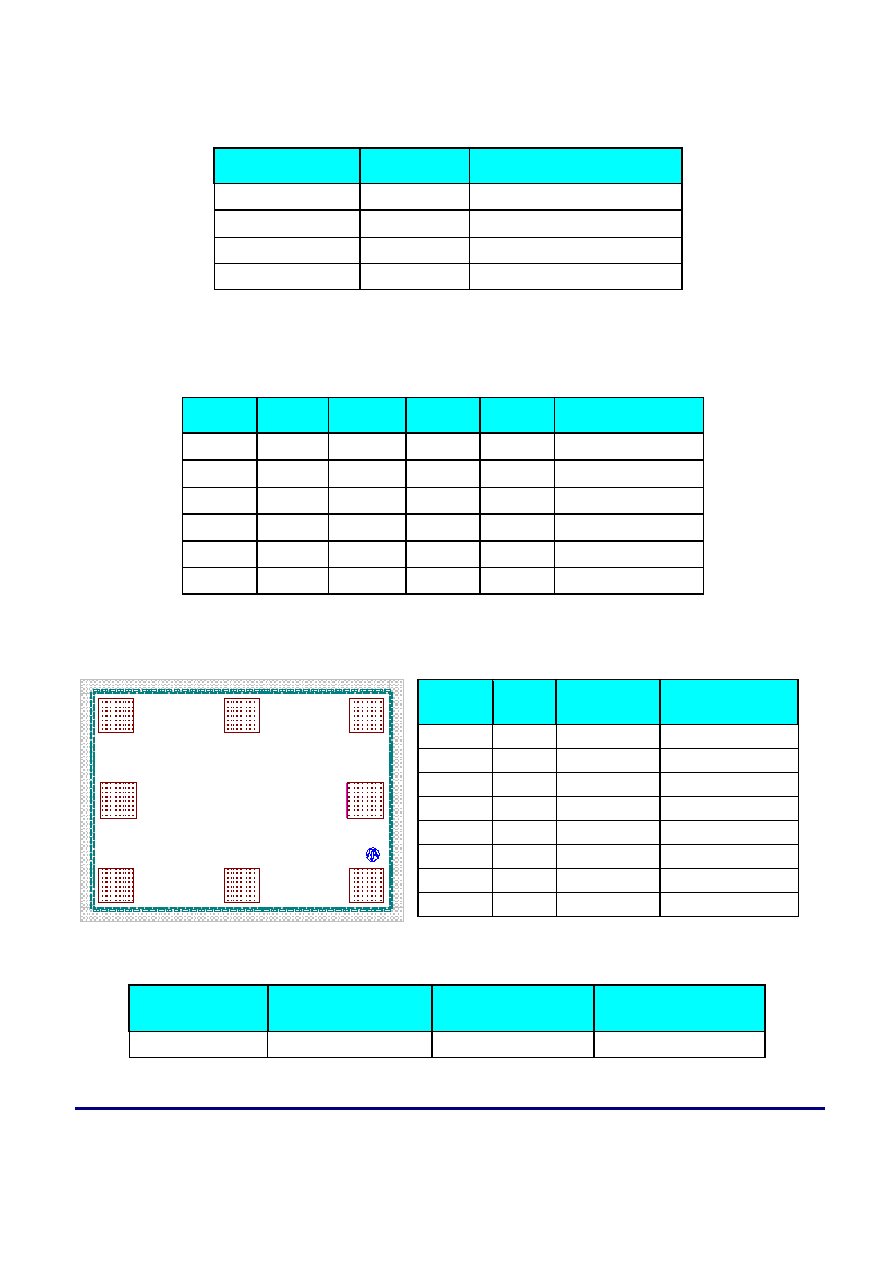
Pad and Die Layout:
Note: Co-ordinates are referenced from the bottom left hand corner of the die to the centre of the
bond pad opening
Die Size (
µm)
Die Thickness (
µm)
Min. Bond Pad
Pitch (
µm)
Min. Bond pad
opening (
µm)
930x600 150
225
85x85
Pad
Ref
Pad
Name
Description
Pin Coordinates
(µm)
A
ANT1
Antenna 1
(155, 300)
B RX Receive
(465,
90)
C
ANT2
Antenna 2
(775, 300)
D TX Transmit
(465,
510)
E
V1
Vctrl1 (A1 to RX)
(155, 90)
F
V2
Vctrl2 (A2 to RX)
(775, 90)
G
V3
Vctrl3 (TX to A2)
(775, 510)
H
V4
Vctrl4 (A1 to TX)
(155, 510)
A
B
C
D
G
F
E
H
Preliminary Data Sheet
2.2
3
Preliminary specifications subject to change without notice
Filtronic Compound Semiconductors Ltd
Contact Details (UK): Tel: +44 (0) 1325 301111 Fax: +44 (0) 1325 306177 Email: sales@filcs.com
Contact Details (USA): Tel: +1 (408) 850 5790 Fax: +1 (408) 850 5766 Email: sales@filcsi.com
Website: www.filcs.com
FMS2017
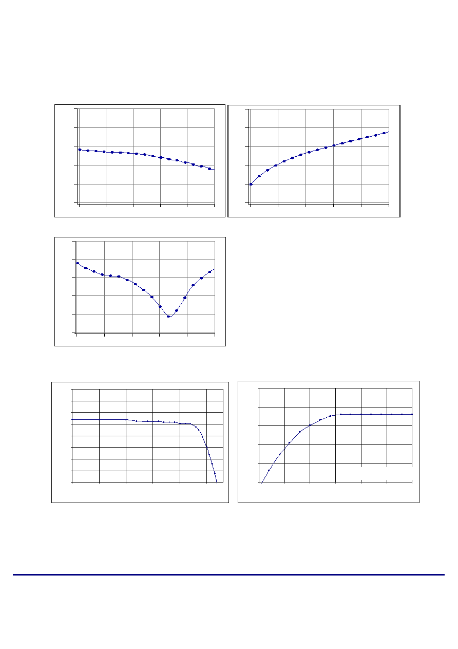
Typical Measured Performance on Evaluation Board (De-Embedded):
(Measurement Conditions V
CTRL
=3V, T
AMBIENT
= 25°C unless otherwise stated)
Insertion Loss
Tx-Rx Isolation
-1 .0
-0 .8
-0 .6
-0 .4
-0 .2
0 .0
I
n
se
r
t
i
o
n Lo
ss (
d
B
)
3.0
2 .5
2.0
1 .5
1.0
0.5
F requ enc y (GH z)
-40
-35
-30
-25
-20
-15
Iso
l
a
t
io
n
(d
B
)
3.0
2 .5
2.0
1 .5
1.0
0 .5
Freque ncy (GH z)
Return Loss
-35
-30
-25
-20
-15
-10
R
e
t
u
rn
L
o
s
s
(d
B
)
3.0
2 .5
2.0
1 .5
1.0
0 .5
Freque ncy (G H z)
Insertion Loss vs Input Power
Insertion Loss vs Control Voltage
-1.6
-1.4
-1.2
-1
-0.8
-0.6
-0.4
-0.2
0
10
15
20
25
30
35
Input Pow er (dBm )
I
n
ser
t
i
o
n
L
o
ss
(
d
B
)
-2
-1.6
-1.2
-0.8
-0.4
0
1.50
1.75
2.00
2.25
2.50
2.75
3.00
Control Voltage (V)
I
n
s
e
r
t
i
on Los
s
(dB
)
Input Power=28dBm
Preliminary Data Sheet
2.2
4
Preliminary specifications subject to change without notice
Filtronic Compound Semiconductors Ltd
Contact Details (UK): Tel: +44 (0) 1325 301111 Fax: +44 (0) 1325 306177 Email: sales@filcs.com
Contact Details (USA): Tel: +1 (408) 850 5790 Fax: +1 (408) 850 5766 Email: sales@filcsi.com
Website: www.filcs.com
FMS2017
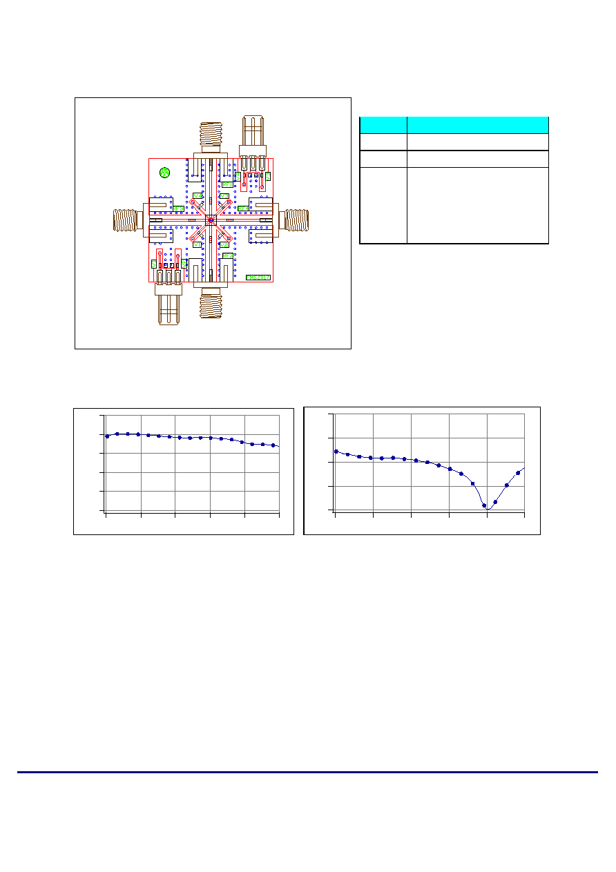
Evaluation Board:
BOM
Evaluation Board De-Embedding Data (Measured):
Insertion Loss
Return Loss
-1.0
-0.8
-0.6
-0.4
-0.2
0.0
I
n
se
r
t
io
n
L
o
ss
(
d
B
)
3.0
2.5
2.0
1.5
1.0
0.5
Frequency (GHz)
-40
-30
-20
-10
0
R
e
t
u
rn
L
o
s
s
(d
B)
3.0
2.5
2.0
1.5
1.0
0.5
Frequency (GHz)
Label
Component
C1
Capacitor, 100pF, 0603
C2 Capacitor,
47pF,
0402
BOARD
Preferred evaluation board material is 0.25
mm thick ROGERS RT4350. All RF tracks
should be 50 ohm characteristic
impedance. Absolute placement of
surface mount de-coupling capacitors is not
critical.
C2
C2
C2
C2
C1
RF3/ANT1
RF4/ANT2
RF1/TX
RF2/RX
V4, GND, V3
V1, GND V2
C1
C1
C1
C2
C2
C2
C2

Preliminary Data Sheet
2.2
5
Preliminary specifications subject to change without notice
Filtronic Compound Semiconductors Ltd
Contact Details (UK): Tel: +44 (0) 1325 301111 Fax: +44 (0) 1325 306177 Email: sales@filcs.com
Contact Details (USA): Tel: +1 (408) 850 5790 Fax: +1 (408) 850 5766 Email: sales@filcsi.com
Website: www.filcs.com
FMS2017
Ordering Information:
Part Number
Description
FMS2017-000-WP
Die waffle pak
FMS2017-000-GP
Die gel pak
FMS2017-000-EB
Die mounted on evaluation board
FMS2017-000-FF
Wafer mounted on film frame
Preferred Assembly Instructions:
GaAs devices are fragile and should be handled with great care. Specially designed collets should be
used where possible.
The back of the die is not metallised and the recommended mounting method is by the use of
conductive epoxy. Epoxy should be applied to the attachment surface uniformly and sparingly to avoid
encroachment of epoxy on to the top face of the die and ideally should not exceed half the chip height.
For automated dispense Ablestick LMISR4 is recommended and for manual dispense Ablestick 84-1
LMI or 84-1 LMIT are recommended. These should be cured at a temperature of 150
°C for 1 hour in
an oven especially set aside for epoxy curing only. If possible the curing oven should be flushed with
dry nitrogen.
This part has gold (Au) bond pads requiring the use of gold (99.99% pure) bondwire. It is
recommended that 25.4
µm diameter gold wire is used. Thermosonic ball bonding is preferred. A
nominal stage temperature of 150
°C and a bonding force of 40g has been shown to give effective
results for 25
µm wire. Ultrasonic energy shall be kept to a minimum. For this bonding technique,
stage temperature should not be raised above 200°C and bond force should not be raised above 60g.
Thermosonic wedge bonding and thermocompression wedge bonding can also be used to achieve
good wire bonds.
Bonds should be made from the die first and then to the mounting substrate or package. The physical
length of the bondwires should be minimised especially when making RF or ground connections.
Handling Precautions:
To avoid damage to the devices care should be exercised during handling. Proper Electrostatic
Discharge (ESD) precautions should be observed at all stages of storage, handling, assembly, and
testing. These devices should be treated as Class 1A (0-500 V) as defined in JEDEC Standard No.
22-A114-B. Further information on ESD control measures can be found in MIL-STD-1686 and MIL-
HDBK-263.
Disclaimers:
This product is not designed for use in any space based or life sustaining/supporting equipment.