 | ÐлекÑÑоннÑй компоненÑ: FMS2022 | СкаÑаÑÑ:  PDF PDF  ZIP ZIP |
Äîêóìåíòàöèÿ è îïèñàíèÿ www.docs.chipfind.ru
Advanced Product Information
1.1
1
Preliminary specifications subject to change without notice
Filtronic Compound Semiconductors Ltd
Contact Details (UK): Tel: +44 (0) 1325 301111 Fax: +44 (0) 1325 306177 Email: sales@filcs.com
Contact Details (USA): Tel: +1 (408) 850 5790 Fax: +1 (408) 850 5766 Email:
sales@filcsi.com
Website: www.filtronic.co.uk/semis
FMS2022
DC4 GHz MMIC SP4T Absorptive Switch
Features:
Available in die form
Suitable for WLAN Applications
Low Insertion loss <1.3 dB at 4 GHz typical
High isolation >30 dB at 4 GHz typical
Absorptive
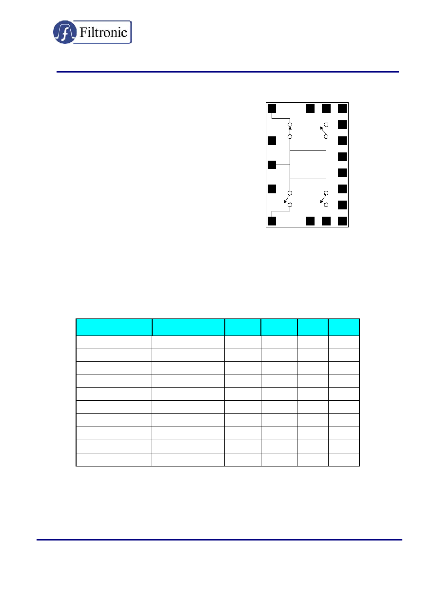
Functional Schematic
OUT1 GND OUT2
IN
A2
GND
GND
OUT4 GND OUT3
B2
A1
B1
A4
B4
A3
B3
Description and Applications:
The FMS2022 is a low loss high isolation DC-4GHz single pole four throw Gallium Arsenide
absorptive switch designed for use in WLAN Applications. The die is fabricated using the Filtronic
FL05 0.5
µm switch process technology that offers leading edge performance optimised for switch
applications.
Simulated Electrical Specifications:
(T
AMBIENT
= 25°C, Vctrl = 0V/-5V), Z
IN
= Z
OUT
= 50
)
Parameter
Conditions
Min
Typ
Max
Units
Insertion Loss
(DC-2) GHz
1
dB
Insertion Loss
(2-4) GHz
1.3
dB
Isolation (DC-2)
GHz
45
dB
Isolation (2-4)
GHz
30
dB
Return Loss (On state)
(DC-4) GHz
17
dB
Return Loss (Off state)
(DC-4) GHz
12
dB
Switching speed
50% control to 10% / 90% RF
25
ns
P1dB (1-100)
MHz
17
dBm
P1dB (100-500)
MHz
24
dBm
P1dB (0.5-40)
GHz
28
dBm
Note: External DC decoupling capacitors are required on all DC lines (typ: 47pF)
Advanced Product Information
1.1
2
Preliminary specifications subject to change without notice
Filtronic Compound Semiconductors Ltd
Contact Details (UK): Tel: +44 (0) 1325 301111 Fax: +44 (0) 1325 306177 Email: sales@filcs.com
Contact Details (USA): Tel: +1 (408) 850 5790 Fax: +1 (408) 850 5766 Email:
sales@filcsi.com
Website:
www.filtronic.co.uk/semis
FMS2022
Truth Table:
Control Lines
RF Path
A1 B1
A2 B2 A3 B3 A4 B4 IN-OUT1 IN-OUT2 IN-OUT3 IN-OUT4
-5V 0V
0V
-5V 0V
-5V
0V
-5V
ON OFF
OFF
OFF
0V
-5V
-5V
0V
0V
-5V
0V
-5V
OFF ON
OFF
OFF
0V
-5V
0V
-5V -5V
0V
0V
-5V
OFF
OFF
ON
OFF
0V
-5V
0V
-5V
0V
-5V -5V
0V
OFF
OFF
OFF
ON
Note: -5V
± 0.5V, 0V+0.5V
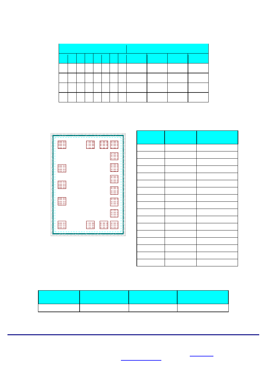
Pad Layout:
Note: Co-ordinates are referenced from the bottom left hand corner of the die to the centre of the
bond pad opening
Die Size
( µm x µm )
Die Thickness (
µm)
Min. Bond Pad
Pitch(
µm)
Min. Bond pad
Opening (
µm xµm )
950 x 1320
150
130
94 x 94
Pad
Reference
Description
Pin Coordinates
(µm)
IN RFIN
142,657.5
OUT1 RFOUT1
142,1174
OUT2 RFOUT2
675,1174
OUT3 RFOUT3
675,141
OUT4 RFOUT4
142,141
A1 A1 805,878
B1 B1 805,731
A2 A2 805,1172
B2 B2 805,1025
A3 A3 805,290
B3 B3 805,143
A4 A4 805,584
B4 B4 805,437
GND1 GND
504,1174
GND2 GND
504,141
GND3 GND
142,869
GND4 GND
142,446
IN
GND3
GND4
A2
B2
A1
B1
A4
B4
A3
B3
OUT1 GND1 OUT2
OUT4 GND2 OUT3
Advanced Product Information
1.1
3
Preliminary specifications subject to change without notice
Filtronic Compound Semiconductors Ltd
Contact Details (UK): Tel: +44 (0) 1325 301111 Fax: +44 (0) 1325 306177 Email: sales@filcs.com
Contact Details (USA): Tel: +1 (408) 850 5790 Fax: +1 (408) 850 5766 Email:
sales@filcsi.com
Website:
www.filtronic.co.uk/semis
FMS2022
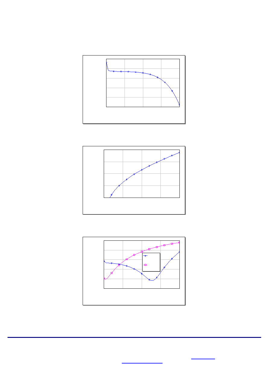
Simulated Performance:
Insertion Loss
0
1
2
3
4
Frequency (GHz)
-1.3
-1.2
-1.1
-1
-0.9
-0.8
I
n
s
e
rt
i
o
n
L
o
s
s
(dB
)
Isolation
0
1
2
3
4
Frequency (GHz)
-70
-60
-50
-40
-30
I
s
ol
at
i
o
n
(
d
B
)
Return Loss
0
1
2
3
4
Frequency (GHz)
-35
-30
-25
-20
-15
-10
Re
tu
r
n
L
o
ss
(
d
B)
On state
Off state

Advanced Product Information
1.1
4
Preliminary specifications subject to change without notice
Filtronic Compound Semiconductors Ltd
Contact Details (UK): Tel: +44 (0) 1325 301111 Fax: +44 (0) 1325 306177 Email: sales@filcs.com
Contact Details (USA): Tel: +1 (408) 850 5790 Fax: +1 (408) 850 5766 Email:
sales@filcsi.com
Website:
www.filtronic.co.uk/semis
FMS2022
Preferred Assembly Instructions:
GaAs devices are fragile and should be handled with great care. Specially designed collets should be
used where possible.
The back of the die is not metallised and the recommended mounting method is by the use of
conductive epoxy. Epoxy should be applied to the attachment surface uniformly and sparingly to avoid
encroachment of epoxy on to the top face of the die and ideally should not exceed half the chip height.
For automated dispense Ablestick LMISR4 is recommended and for manual dispense Ablestick 84-1
LMI or 84-1 LMIT are recommended. These should be cured at a temperature of 150
°C for 1 hour in
an oven especially set aside for epoxy curing only. If possible the curing oven should be flushed with
dry nitrogen.
This part has gold (Au) bond pads requiring the use of gold (99.99% pure) bondwire. It is
recommended that 25.4
µm diameter gold wire is used. Thermosonic ball bonding is preferred. A
nominal stage temperature of 150
°C and a bonding force of 40g has been shown to give effective
results for 25
µm wire. Ultrasonic energy shall be kept to a minimum. For this bonding technique,
stage temperature should not be raised above 200°C and bond force should not be raised above 60g.
Thermosonic wedge bonding and thermocompression wedge bonding can also be used to achieve
good wire bonds.
Bonds should be made from the die first and then to the mounting substrate or package. The physical
length of the bondwires should be minimised especially when making RF or ground connections.
Handling Precautions:
To avoid damage to the devices care should be exercised during handling. Proper Electrostatic
Discharge (ESD) precautions should be observed at all stages of storage, handling, assembly, and
testing. These devices should be treated as Class 1A (0-500 V) as defined in JEDEC Standard No.
22-A114-B. Further information on ESD control measures can be found in MIL-STD-1686 and MIL-
HDBK-263.
Disclaimers:
This product is not designed for use in any space based or life sustaining/supporting equipment.