PRELIMINARY DATA SHEET
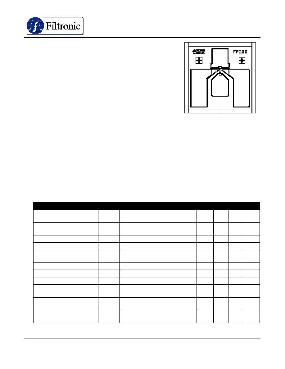
FP100
H
IGH
P
ERFORMANCE
PHEMT
Phone: (408) 988-1845
http:// www.filss.com
Email: sales@filss.com
Fax: (408) 970-9950
Revised: 07/18/01
∑
FEATURES
14 dBm P-1dB at 12 GHz
9 dB Power Gain at 12 GHz
3.0 dB Noise Figure at 12 GHz
DIE SIZE: 16.5 x 16.5 mils (420 x 420
µ
m)
DIE THICKNESS: 3.9 mils (100
µ
m typ.)
BONDING PADS: 3.3 x 3.5 mils (85 x 90
µ
m typ.)
∑
DESCRIPTION AND APPLICATIONS
The FP100 is an Aluminum Gallium Arsenide / Indium Gallium Arsenide (AlGaAs/InGaAs)
Pseudomorphic High Electron Mobility Transistor (PHEMT), utilizing an Electron-Beam direct-
write 0.25 um by 100 um Schottky barrier gate. The recessed "mushroom" gate structure minimizes
parasitic gate-source and gate resistances. The FP100 features Si3N4 passivation.
Typical applications include general purpose, low noise and broadband amplifiers in the 2-20 GHz
range. The device is well-suited for telecommunication applications.
∑
ELECTRICAL SPECIFICATIONS @ T
Ambient
= 22 ± 3 ∞C
Parameter
Symbol
Test Conditions
Min
Typ
Max
Units
Output Power @
1 dB Compression
P
1dB
f = 12 GHz; V
DS
= 5V; I
DS
= 50% I
DSS
13
14
dBm
Power Gain @
1 dB Compression
G
1dB
f = 12 GHz; V
DS
= 5V; I
DS
= 50% I
DSS
8
9
dB
Maximum Available Gain
MAG
f = 12 GHz; V
DS
= 5V; I
DS
= 50% I
DSS
14.5
15.5
dB
Noise Figure
NF
f = 12 GHz; V
DS
= 5V; I
DS
= 50% I
DSS
3.0
dB
Power-Added Efficiency
f = 12 GHz; V
DS
= 5V; I
DS
= 50% I
DSS
;
P
OUT
= 15.5 dBm
20
25
%
Saturated Drain-Source Current
I
DSS
V
DS
= 2 V; V
GS
= 0 V
15
30
mA
Transconductance
G
M
V
DS
= 2 V; V
GS
= 0 V
15
20
mS
Pinch-Off Voltage
V
P
V
DS
= 2 V; I
DS
= 1 mA
-0.50
-2.5
V
Gate-Drain Breakdown
Voltage Magnitude
|V
BDGD
|
I
GS
= 1 mA
8
10.5
V
Gate-Source Breakdown
Voltage Magnitude
|V
BDGS
|
I
GS
= 1 mA
7
10
V
Gate-Source Leakage
Current Magnitude
|I
GSL
|
V
GS
= -5 V
4
10
µ
A

PRELIMINARY DATA SHEET
FP100
H
IGH
P
ERFORMANCE
PHEMT
Phone: (408) 988-1845
http:// www.filss.com
Email: sales@filss.com
Fax: (408) 970-9950
Revised: 07/18/01
∑
RECOMMENDED CONTINUOUS OPERATING LIMITS
Parameter
Symbol
Nominal
Units
Drain-Source Voltage
V
DS
5
V
Gate-Source Voltage
V
GS
-0.8
V
Drain-Source Current
I
DS
0.5 I
DSS
mA
RF Input Power
P
IN
30
mW
Channel Operating Temperature
T
CH
150
∞
C
Ambient Temperature
T
STG
-20/50
∞
C
Note:
Device should be operated at or below Recommended Continuous Operating Limits for reliable performance.
∑
ABSOLUTE RATINGS
Parameter
Symbol
Test Conditions
Min
Max
Units
Drain-Source Voltage
V
DS
T
Ambient
= 22
±
3
∞
C
7
V
Gate-Source Voltage
V
GS
T
Ambient
= 22
±
3
∞
C
-3
V
Drain-Source Current
I
DS
T
Ambient
= 22
±
3
∞
C
I
DSS
mA
Gate Current
I
G
T
Ambient
= 22
±
3
∞
C
2.5
mA
RF Input Power
P
IN
T
Ambient
= 22
±
3
∞
C
60
mW
Channel Operating Temperature
T
CH
T
Ambient
= 22
±
3
∞
C
175
∫C
Storage Temperature
T
STG
--
-65
175
∫C
Note:
Even temporary operating conditions that exceed the Absolute Maximum Ratings could result in permanent damage
to the device.
∑
APPLICATIONS NOTES & DESIGN DATA
Applications Notes are available from your local Filtronic Sales Representative or directly from the
factory. Complete design data, including S-parameters, noise data, and large-signal models are
available on the Filtronic web site.
∑
HANDLING PRECAUTIONS
To avoid damage to the devices care should be exercised during handling. Proper Electrostatic
Discharge (ESD) precautions should be observed at all stages of storage, handling, assembly, and
testing. These devices should be treated as Class 1A (0-500 V). Further information on ESD control
measures can be found in MIL-STD-1686 and MIL-HDBK-263.
All information and specifications are subject to change without notice.