 | –≠–ª–µ–∫—Ç—Ä–æ–Ω–Ω—ã–π –∫–æ–º–ø–æ–Ω–µ–Ω—Ç: LMA406 | –°–∫–∞—á–∞—Ç—å:  PDF PDF  ZIP ZIP |

LMA406
L
OW
N
OISE
PHEMT
MMIC
Phone: (408) 988-1845
http:// www.filss.com
Revised: 12/5/00
Fax: (408) 970-9950
Email: sales@filss.com
∑
FEATURES
18 GHz to 40 GHz Frequency Band
4.5 dB Noise Figure
12dB Gain
14 dBm Output Power at Saturation
+3 V Single Bias Supply
∑
DESCRIPTION AND APPLICATIONS
The Filtronic Solid State LMA406 is a low noise PHEMT amplifier that operates from 18 to 40GHz.
This 2-stage amplifier provides 12dB nominal gain with 4.5dB typical noise figure and 1-dB gain
compression power output of +10dBm that is designed for commercial mmW (millimeter-wave)
PCN/PCS applications. Ground is provided to the circuitry through vias to the backside
metallization.
∑
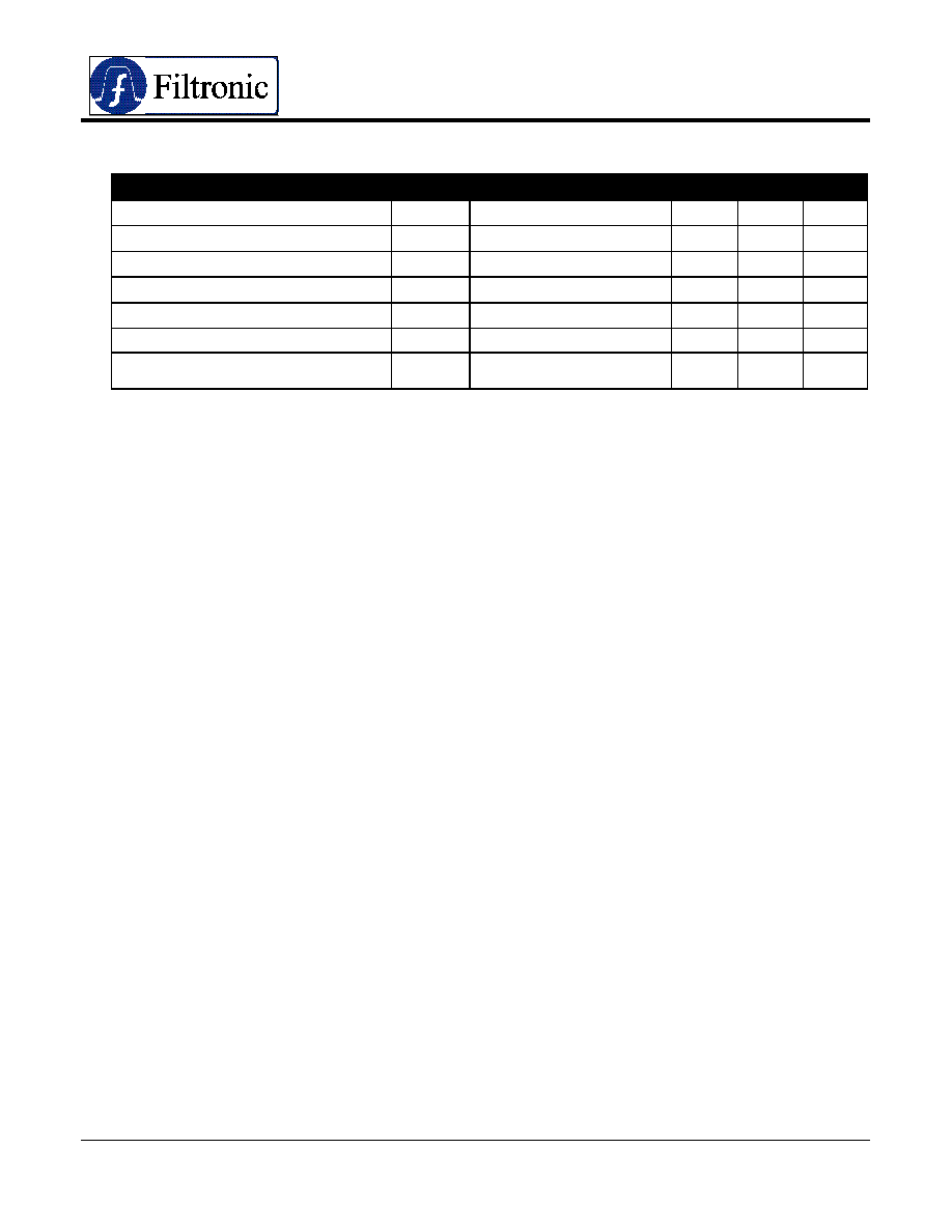
ELECTRICAL SPECIFICATIONS @ T
Ambient
= 25∞C
(V
DD
= +3.0V, Z
IN
= Z
OUT
= 50
)
Parameter
Symbol
Test Conditions
Min
Typ
Max
Units
Frequency Band
F
18
40
GHz
Small Signal Gain
S
21
30% I
DSS
(Pad B&D Ground)
9
11.5
dB
30% I
DSS
(Pad A&C Ground)
9
12.5
dB
Saturated Drain Current
I
DSS
R
S
= 0/0
40
80
120
mA
Small Signal Gain Flatness
S
21
±
1
±
2.5
dB
Noise Figure
NF
50% I
DSS
4.5
6.0
dB
Input Return Loss
S
11
-12
dB
Output Return Loss
S
22
-14
dB
Reverse Isolation
S
12
-32
-38
dB
LMA406
L
OW
N
OISE
PHEMT
MMIC
Phone: (408) 988-1845
http:// www.filss.com
Revised: 12/5/00
Fax: (408) 970-9950
Email: sales@filss.com
∑
ABSOLUTE MAXIMUM RATINGS
Parameter
Symbol
Test Conditions
Min
Max
Units
Drain Voltage
V
D
T
Ambient
= 22
±
3
∞
C
4
V
Operating Current
I
OP
T
Ambient
= 22
±
3
∞
C
120
mA
RF Input Power
P
IN
T
Ambient
= 22
±
3
∞
C
10
dBm
Total Power Dissipation
P
TOT
T
Ambient
= 22
±
3
∞
C
.48
W
Channel Operating Temperature
T
CH
T
Ambient
= 22
±
3
∞
C
150
∫C
Storage Temperature
T
STG
--
-65
165
∫C
Maximum Assembly Temperature
(1 min. max.)
T
MAX
--
300
∫C
Notes:
∑
Operating conditions that exceed the Absolute Maximum Ratings could result in permanent damage to the device.
∑
Recommended Continuous Operating Limits should be observed for reliable device operation.
∑
Power Dissipation defined as: P
TOT
(P
DC
+ P
IN
) ≠ P
OUT
, where
P
DC
: DC Bias Power
P
IN
: RF Input Power
P
OUT
: RF Output Power
∑
This GaAs MMIC is susceptible to damage from Electrostatic Discharge. Proper precautions should be used when
handling these devices.
LMA406
L
OW
N
OISE
PHEMT
MMIC
Phone: (408) 988-1845
http:// www.filss.com
Revised: 12/5/00
Fax: (408) 970-9950
Email: sales@filss.com
∑
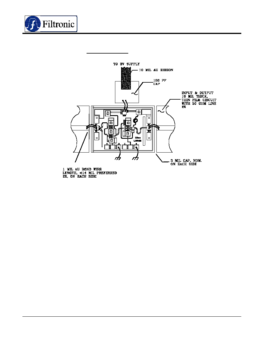
ASSEMBLY DRAWING
LOW NOISE BIAS: PAD B & D TO GND
Notes:
∑
Recommended lead bond technique is thermocompression wedge bonding with 0.001" (25µm) diameter wire. The
bond tool force shall be 35-38 gram. Bonding stage temperature shall be 230-240∞C, heated tool (150-160∞C) is
recommended. Ultrasonic bonding is not recommended.
∑
The recommended die attach is Ablebond silver epoxy, the stabilize bake temperature is set at 150∞C for 45 minutes.
∑
Bond on bond or stitch bond acceptable.
∑
Conductor over conductor acceptable. Conductors must not short.

LMA406
L
OW
N
OISE
PHEMT
MMIC
Phone: (408) 988-1845
http:// www.filss.com
Revised: 12/5/00
Fax: (408) 970-9950
Email: sales@filss.com
∑
ASSEMBLY DRAWING
HIGH GAIN BIAS:
PAD A & C TO GND
Notes:
∑
Recommended lead bond technique is thermocompression wedge bonding with 0.001" (25µm) diameter wire. The
bond tool force shall be 35-38 gram. Bonding stage temperature shall be 230-240∞C, heated tool (150-160∞C) is
recommended. Ultrasonic bonding is not recommended.
∑
The recommended die attach is Ablebond silver epoxy, the stabilize bake temperature is set at 150∞C for 45 minutes.
∑
Bond on bond or stitch bond acceptable.
∑
Conductor over conductor acceptable. Conductors must not short.
LMA406
L
OW
N
OISE
PHEMT
MMIC
Phone: (408) 988-1845
http:// www.filss.com
Revised: 12/5/00
Fax: (408) 970-9950
Email: sales@filss.com
∑
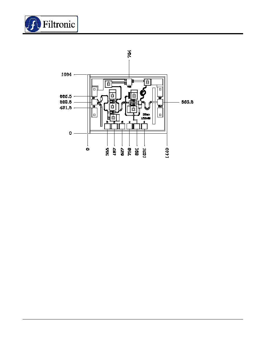
MECHANICAL OUTLINE
Notes:
∑
All units are in microns (µm).
∑
All bond pads are 100 X 100 µm
2
.
∑
Bias pad (V
DD
) size is 100 X 121.5 µm
2
.
∑
Unless otherwise specified.
∑
HANDLING PRECAUTIONS
To avoid damage to the devices care should be exercised during handling. Proper Electrostatic
Discharge (ESD) precautions should be observed at all stages of storage, handling, assembly, and
testing. These devices should be treated as Class 1A (0-500 V). Further information on ESD control
measures can be found in MIL-STD-1686 and MIL-HDBK-263.
All information and specifications are subject to change without notice.