Filtronic
LPV1500
Solid State
1 W Power PHEMT
Phone: (408) 988-1845 Internet:
http://www.filtronicsolidstate.com
Fax: (408) 970-9950
FEATURES
∑
+31.5 dBm Typical Power at 18 GHz
∑
8.5 dB Typical Power Gain at 18 GHz
∑
+27 dBm at 3.3V Battery Voltage
∑
+45 dBm Typical Intercept Point
∑
50% Power-Added-Efficiency at 18 GHz
∑
Plated Source Thru-Vias
DIE SIZE: 16.5 x 16.1 mils (420 x 410
µ
m)
DIE THICKNESS: 3.0 mils (75
µ
m typ.)
BONDING PADS: 1.9 x 2.4 mils (50 x 60
µ
m typ.)
DESCRIPTION AND APPLICATIONS
The LPV1500 is an Aluminum Gallium Arsenide / Indium Gallium Arsenide (AlGaAs/InGaAs) Pseudomorphic High
Electron Mobility Transistor (PHEMT), utilizing an Electron-Beam direct-write 0.25
µ
m by 1500
µ
m Schottky barrier gate.
The recessed "mushroom" gate structure minimizes parasitic gate-source and gate resistances. The epitaxial structure
and processing have been optimized for reliable high-power applications. The LP1V500 also features Si
3
N
4
passivation
and is available in a flanged ceramic package (P100). The LPV1500 features plated source thru-vias for improved
performance.
Typical applications include commercial and military high-performance power amplifiers, including SATCOM uplink
transmitters, PCS/Cellular low-voltage high-efficiency output amplifiers, and medium-haul digital radio transmitters. The
LP1500 may be procured in a variety of grades, depending upon specific user requirements. Standard lot screening is
patterned after MIL-STD-19500, JANC grade. Space-level screening to FSS JANS grade is also available.
PERFORMANCE SPECIFICATIONS (T
A
= 25
∞
C)
SYMBOLS
PARAMETERS
MIN
TYP
MAX
UNITS
I
DSS
Saturated Drain-Source Current
V
DS
= 2V V
GS
= 0V
375
490
600
mA
P
1dB
Output Power at 1dB Gain Compression
V
DS
= 8.0V, I
DS
= 50% I
DSS
f
= 18 GHz
30.0
31.5
dBm
G
1dB
Power Gain at 1dB Gain Compression
V
DS
= 8.0V, I
DS
= 50% I
DSS
f
= 18 GHz
6.5
8.5
dB
IP3
Output 3rd-Order Intercept Pt.
V
DS
= 8V, I
DS
= 40% I
DSS
,
45
dBm
ADD
Power-Added Efficiency
50
%
I
MAX
Maximum Drain-Source Current
V
DS
= 2V V
GS
= +1V
925
mA
G
M
Transconductance
V
DS
= 2V V
GS
= 0V
350
450
mS
V
P
Pinch-Off Voltage
V
DS
= 2V I
DS
= 5mA
-0.25
-1.2
-2.0
V
I
GSO
Gate-Source Leakage Current
V
GS
= -5V
10
75
µ
A
BV
GS
Gate-Source Breakdown Voltage
I
GS
= 8mA
-12
-15
V
BV
GD
Gate-Drain Breakdown Voltage
I
GD
= 8mA
-12
-16
V
J
Thermal Resistivity
45
∞
C/W
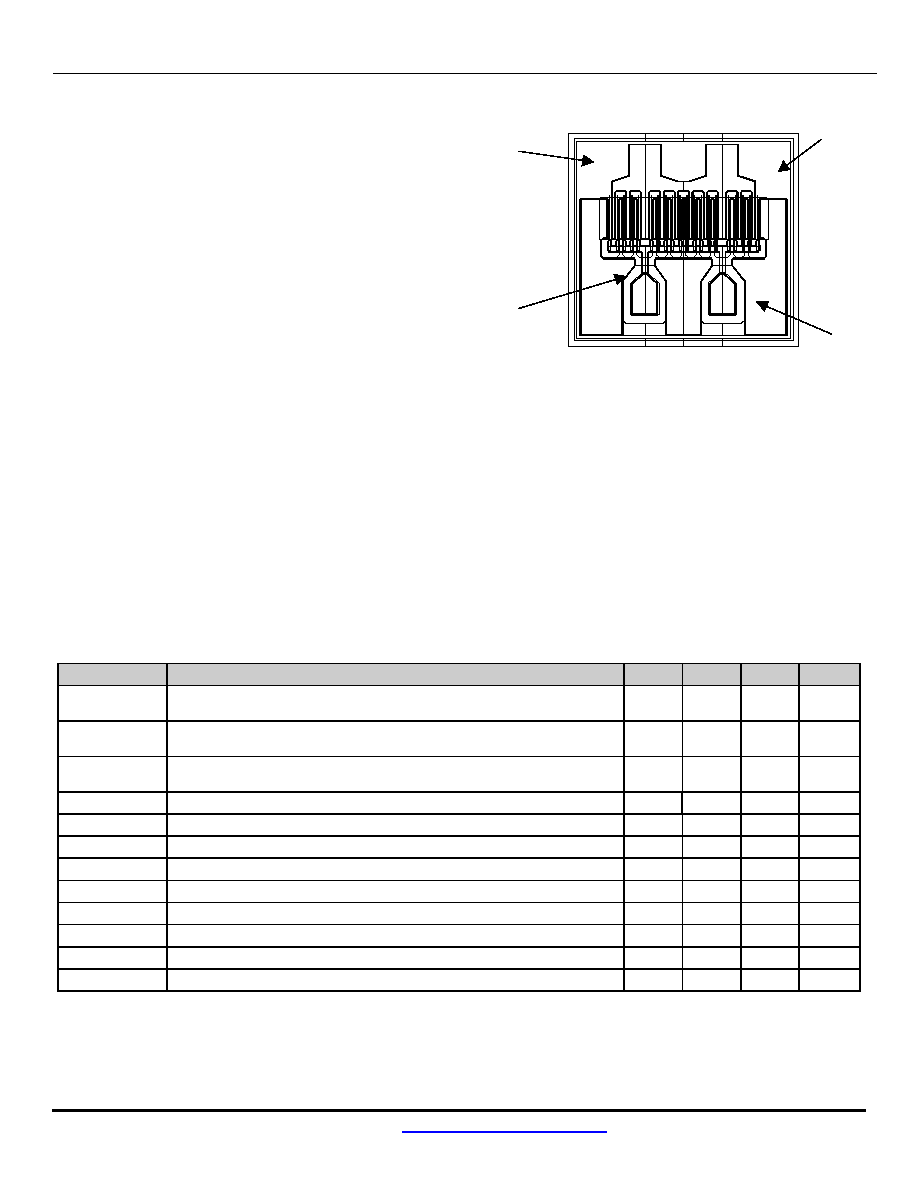
DSS-041 WA
DRAIN
SOURCE
GATE
DRAIN
Filtronic
LPV1500
Solid State
1 W Power PHEMT
Phone: (408) 988-1845 Internet:
http://www.filtronicsolidstate.com
Fax: (408) 970-9950
ABSOLUTE MAXIMUM RATINGS
(25
∞
C)
RECOMMENDED CONTINUOUS
OPERATING LIMITS
SYMBOL
PARAMETER
RATING
1
SYMBOL
PARAMETER
RATING
2
V
DS
Drain-Source Voltage
+12V
V
DS
Drain-Source Voltage
+8V
V
GS
Gate-Source Voltage
-5V
V
GS
Gate-Source Voltage
-1V
I
DS
Drain-Source Current
2 x I
DSS
I
DS
Drain-Source Current
0.8 x I
DSS
I
G
Gate Current
70 mA
I
G
Gate Current
15 mA
P
IN
RF Input Power
750 mW
P
IN
RF Input Power
300 mW
T
CH
Channel Temperature
+175
∞
C
T
CH
Channel Temperature
+150
∞
C
T
STG
Storage Temperature
-65/175
∞
C
T
STG
Storage Temperature
-20/50
∞
C
P
T
Power Dissipation
3.33W
3,4
P
T
Power Dissipation
3.0 W
3,4
G
XdB
Gain Compression
8 dB
NOTES:
1. Operating conditions that exceed the Absolute Maximum Ratings could result in permanent damage to the device.
2. Recommended Continuous Operating Limits should be observed for reliable device operation.
3. Power Dissipation defined as: P
T
(P
DC
+ P
IN
) - P
OUT
, where: P
DC
= DC bias power, P
OUT
= RF output power, and
P
IN
= RF input power.
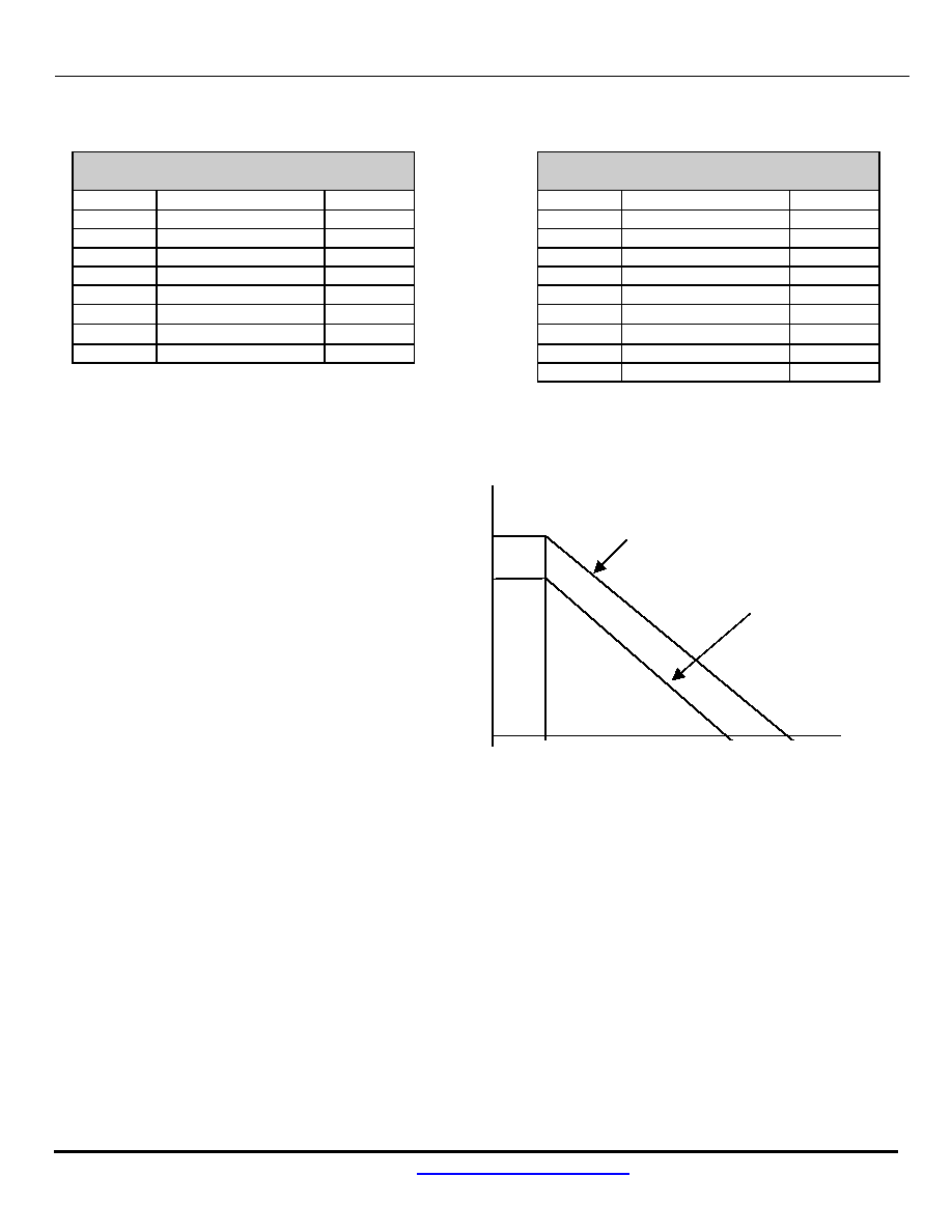
4. Power Dissipation to be de-rated as follows:
5. Specifications subject to change without notice.
Example #1:
V
DS
= 8V, I
DS
= 315 mA
P
IN
= P
OUT
= 0 dBm (quiescent condition):
P
T
= P
DC
= 2.52W
Max. continuous T
HS
= 37
∞
C
Example #2:
V
DS
= 8V, I
DS
= 315 mA
P
IN
= 23 dBm P
OUT
= 31 dBm
P
T
= (2.52+0.2) - 1.26 = 1.46W
Max. continuous T
HS
= 84
∞
C
HANDLING PRECAUTIONS:
PHEMT chips should be stored in a dry nitrogen environment until assembly. Care should be exercised during handling to
avoid damage to the devices. Proper Electrostatic Discharge (ESD) precautions should be observed at all stages of
storage, handling, assembly, and testing. These devices should be treated as Class 1A (0-500V), and further information
on ESD control measures can be found in MIL-STD-1686 and MIL-HDBK-263.
ASSEMBLY INSTRUCTIONS:
The recommended die attach is gold/tin eutectic solder under a nitrogen atmosphere. Stage temperature should be 280-
290
∞
C; maximum time at temperature is 1 min. The recommended wire bond method is thermo-compression wedge
bonding with 0.7 or 1.0 mil (0.018 or 0.025 mm) gold wire. Stage temperature should be 250-260
∞
C.
APPLICATIONS NOTES AND DESIGN DATA:
Applications Notes are available from your local FSS Sales Representative, or directly from the factory. Complete design
data, including S-parameters, Noise data, and Large-Signal models, is available on 3.5" diskette, or may be down-loaded
from our Web Page.
DSS-041 WA
T
HS
(
o
C)
-22-22 mW/
o
C
mW/
o
C
-24 mW/
o
C
P
T
(W)
3.33
3.0
3.0
25
150
175
175