ChipFind - документация

Электронный компонент: EK7010TCE-1401

Скачать:  PDF   ZIP
CONFIDENTIAL


DOC NO
TDS70 0-05
REV
.
DOC Title
EK7010TCE-140P1
Page
/
/
Revision History
REV.
REV Date
Eff. Date
REV. Page
/
/
Revise item / Content
.0
.
2001/12/18
2002/3/25
200 / 2/28
P.2
.
Pin configuration.
CONFIDENTIAL
Microelectronics, Inc.
EK7010TCE-140P1
240 Output STN
Segment & Common LCD Driver
Eureka
6F, NO.12, INNOVATION 1
ST
. RD.,
SCIENCE-BASED INDUSTRIAL PARK, HSIN-CHU
CITY, TAIWAN, R.O.C.
TEL
886-3-5799255
FAX
886-3-5799253
http://www.eureka.com.tw
CONFIDENTIAL
EUREKA
EK7010TCE-140P1
1 Rev 1.1 Mar.25.2002
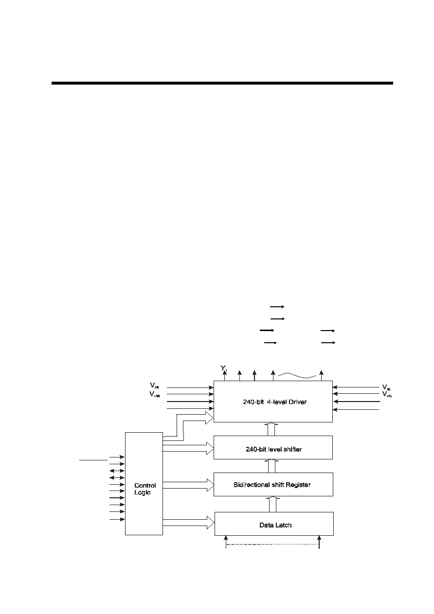
Description
The EK7010 is a 240 output segment/common LCD
driver adaptable to drive a large scale dot matrix panel.
It uses the Tape Carrier Package(TCP) to greatly
reduce the size of the LCD module. EK7010 consumes
very little power. Large LCD panels can be assembled
by cascading EK7010s. In Segment Mode, the input
data can be either 4-bit parallel or 8-bit parallel, selected
by the Mode Select pin (MD).
240 Output Segment/Common LCD Driver
Features
CMOS process
Logic power supply : 2.5V to 5.5V
Low power consumption
240 LCD display output
Supply voltage for LCD driver :15 to 40V
Package : TCP, COG available
Features in Segment mode
Shift clock frequency : 20MHz max. at V
DD
= 5V
4bit/8bit parallel input
Automatic transfer of enable signal
Automatic counting in the chip select mode. The
internal clock is stoped by automatically counting
240 of input data.
Features in Common mode
Shift clock frequency : 4MHz max. at V
DD
=5V
Built-in 240-bit bidirectional shift register
Single mode (240-bit shift register) or Dual Mode
(two 120-bit shift registers) with these options:
1. Y1 Y240 Single mode
2. Y240 Y1 Single mode
3. Y1 Y120, Y121 Y240 Dual mode
4. Y240 Y121, Y120 Y1 Dual mode
Y
2
Y
3
Y
4
Y
240
XCK
L/R
MD
S/C
V
12R
V
0R
V
12L
V
0L
DI
0
DI
7
FR
DISPOFF
EIO
1
LP
EIO
2
TEST1
Block Diagram
Fig.1
CONFIDENTIAL
EUREKA
EK7010TCE-140P1
2 Rev 1.1 Mar.25.2002
Pin Configuration
Fig.2
V
0L
12
L
43
L
5L
DD
2
0
1
2
3
4
5
6
7
1
1
SS
5R
43
R
12
R
0R
V
V
V
Dum
m
y
V
S/
C
EI
O
DI
DI
DI
DI
DI
DI
DI
DI
XC
K
LP
EI
O
FR
L/R
MD
TE
ST
V
Dum
m
y
V
V
V
V
V
0L
0R
V
DI
S
P
O
F
F
242...................................................................................................................................................1
Du
m
m
y
Y
Y
Y
24
0
15
9
15
8
Y
Y
Y
Du
m
m
y
3
2
1
Chip Surface
CONFIDENTIAL
EUREKA
EK7010TCE-140P1
3 Rev 1.1 Mar.25.2002
Pin Designations
Tab.1
.
o
N
n
i
P
l
o
b
m
y
S
O
/
I
n
o
i
t
a
n
g
i
s
e
D
1
4
2
o
t
2
Y
1
Y
-
0
4
2
O
t
u
p
t
u
o
D
C
L
,
4
7
2
,
5
4
2
,
4
4
2
5
7
2
V
L
0
V
,
R
0
-
l
e
v
e
l
r
e
v
i
r
d
D
C
L
r
o
f
y
l
p
p
u
s
r
e
w
o
P
3
7
2
,
6
4
2
V
L
2
1
V
,
R
2
1
-
l
e
v
e
l
r
e
v
i
r
d
D
C
L
r
o
f
y
l
p
p
u
s
r
e
w
o
P
2
7
2
,
7
4
2
V
L
3
4
V
,
R
3
4
-
l
e
v
e
l
r
e
v
i
r
d
D
C
L
r
o
f
y
l
p
p
u
s
r
e
w
o
P
1
7
2
,
8
4
2
V
L
5
V
,
R
5
-
l
e
v
e
l
r
e
v
i
r
d
D
C
L
r
o
f
y
l
p
p
u
s
r
e
w
o
P
9
6
2
V
S
S
-
d
n
u
o
r
G
0
5
2
V
D
D
-
)
V
5
.
5
+
o
t
5
.
2
+
(
t
i
u
c
r
i
c
c
i
g
o
l
r
o
f
y
l
p
p
u
s
r
e
w
o
P
1
5
2
C
/
S
I
n
o
i
t
c
e
l
e
s
e
d
o
m
n
o
m
m
o
c
/
e
d
o
m
t
n
e
m
g
e
S
2
5
2
O
I
E
2
O
/
I
r
e
t
s
i
g
e
r
t
f
i
h
s
f
o
a
t
a
d
r
o
t
c
e
l
e
s
p
i
h
c
r
o
f
t
u
p
t
u
o
/
t
u
p
n
I
9
5
2
o
t
3
5
2
I
D
0
I
D
-
6
I
e
d
o
m
t
n
e
m
g
e
s
n
i
a
t
a
d
y
a
l
p
s
i
d
f
o
t
u
p
n
I
0
6
2
I
D
7
I
t
u
p
n
i
a
t
a
d
e
d
o
m
l
a
u
D
r
o
,
e
d
o
m
t
n
e
m
g
e
S
r
o
f
a
t
a
d
y
a
l
p
s
i
d
f
o
t
u
p
n
I
.
e
d
o
m
n
o
m
m
o
c
r
o
f
1
6
2
K
C
X
I
e
d
o
m
t
n
e
m
g
e
s
n
i
t
u
p
n
i
k
c
o
l
c
t
f
i
h
s
a
t
a
d
y
a
l
p
s
i
D
2
6
2
F
F
O
P
S
I
D
I
l
e
v
e
l
t
u
p
t
u
o
t
c
e
l
e
s
e
d
o
t
t
u
p
n
i
n
i
p
l
o
r
t
n
o
C
3
6
2
P
L
I
e
d
o
m
t
n
e
m
g
e
s
n
i
t
u
p
n
i
e
s
l
u
p
h
c
t
a
L
e
d
o
m
d
n
o
m
m
o
c
n
i
r
e
t
s
i
g
e
r
t
f
i
h
s
r
o
f
t
u
p
n
i
k
c
o
l
c
t
f
i
h
S
4
6
2
O
I
E
1
O
/
I
r
e
t
s
i
g
e
r
t
f
i
h
s
f
o
a
t
a
d
r
o
t
c
e
l
e
s
p
i
h
c
r
o
f
t
u
p
t
u
o
/
t
u
p
n
I
5
6
2
R
F
I
m
r
o
f
e
v
a
w
r
e
v
i
r
d
D
C
L
r
o
f
t
u
p
n
i
l
a
n
g
i
s
g
n
i
t
r
e
v
n
o
c
-
C
A
6
6
2
R
/
L
I
n
o
i
t
c
e
l
e
s
n
o
i
t
c
e
r
i
d
t
f
i
h
s
a
t
a
d
y
a
l
p
s
i
D
7
6
2
D
M
I
n
o
i
t
c
e
l
e
s
e
d
o
M
8
6
2
T
S
E
T
1
I
n
o
i
t
c
e
l
e
s
e
d
o
m
t
s
e
T
,
3
4
2
,
2
4
2
,
1
6
7
2
,
0
7
2
,
9
4
2
y
m
m
u
D
-
S
D
A
P
y
m
m
u
D