CONFIDENTIAL
DOC NO
TDS70 -02
REV
.4
DOC Title
EK7011CG DATA SHEET
Page
/
/
Revision History
REV.
REV Date
Eff. Date
REV. Page
/
/
Revise item / Content
0.2
1.1
.2
.3
.4
2000/11/2
2000/11/29
2000/12/6
2001/2/22
2001/10/22
2000/12/07
2000/12/07
2000/12/07
2001/03/05
2001/10/24
29
18
29
34
36
2
28
29
3,4,5,6,7,8,16
17,18,19,20,22
26
16
5
1.
Wafer thickness & Height of Bump
. modify Input voltage condition
2. Add COG application note
3. Separate V
SS
and V
GND
pads
1.
Pin Configuration
2.
logo
3.
Bump Height
4.
HV Ground
V
GND
.
Storage temperature
Operating temperature
CONFIDENTIAL
Microelectronics, Inc.
EK7011CG
160 Output Segment & Common
LCD Driver
Eureka
6F, NO.12, INNOVATION 1
ST
. RD.,
SCIENCE-BASED INDUSTRIAL PARK, HSIN-CHU
CITY, TAIWAN, R.O.C.
TEL
886-3-5799255
FAX
886-3-5799253
http://www.eureka.com.tw
CONFIDENTIAL
EUREKA
EK7011CG
1 Rev 1.4 Oct.22.2001
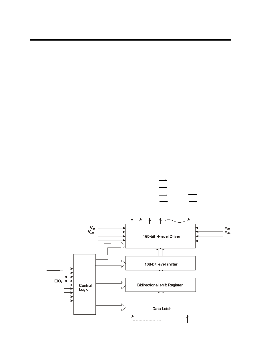
Description
The EK7011 is a 160 output segment/common LCD
driver adaptable to drive a large scale dot matrix panel.
It uses the Tape Carrier Package(TCP) to greatly
reduce the size of the LCD module. EK7011 consumes
very little power. Large LCD panels can be assembled
by cascading EK7011s. In Segment Mode, the input
data can be either 4-bit parallel or 8-bit parallel, selected
by the Mode Select pin (MD).
160 Output Segment/Common LCD Driver
Features
l
CMOS process
l
Logic power supply : 2.5V to 5.5V
l
Low power consumption
l
160 LCD display output
l
Supply voltage for LCD driver :15 to 40V
l
Package : TCP, COG available
Features in Segment mode
l
Shift clock frequency : 14MHz max. at V
DD
=5V
l
4bit/8bit parallel input
l
Automatic transfer of enable signal
l
Automatic counting in the chip select mode. The
internal clock stoped by automatically counting
160 of input data.
Features in Common mode
l
Shift clock frequency : 4MHz max. at V
DD
=5V
l
Built-in 160-bit bidirectional shift register
l
Single mode (160-bit shift register) or Dual Mode
(two 80-bit shift registers) with these options:
1. Y1 Y160 Single mode
2. Y160 Y1 Single mode
3. Y1 Y80, Y81 Y160 Dual mode
4. Y160 Y81, Y80 Y1 Dual mode
Y
1
Y
2
Y
3
Y
4
Y
1 60
X C K
L/R
M D
S /C
V
1 2R
V
0 R
V
1 2L
V
0 L
D I
0
D I
7
F R
D IS P O F F
E IO
1
LP
Block Diagram
Fig.1