
DOC NO TDS7308-01
REV 0.1
DOC Title
EK7308 Preliminary DATA SHEET
Page 1 / 1
/ Revision History
REV.
REV Date
Eff. Date
REV. Page
//
Revise item / Content
0.1 2003/06/09
2003/06/19
New
Issue

EUREKA Microelectronics, Inc.
EK7308
240-Output TFT Gate Driver IC
6F, NO.12, INNOVATION 1
ST
. RD.,
SCIENCE-BASED INDUSTRIAL PARK,
HSIN-CHU CITY, TAIWAN, R.O.C.
http://www.eureka.com.tw

EUREKA
EK7308
June 2003
- 1 - Preliminary Rev 0.1
Table of Contents
Page
1.GENERAL DESCRIPTION
.....................................................................
2
2.FEATURES
...........................................................................................
2
3.BLOCK DIAGRAM
..............................................................................
2
4 PIN FUNCTION DESCRIPTIONS
..............................................................
3
5.FUNCTION OPERATIONS
.......................................................................
4
6.ABSOLUTE MAXIMUM RATINGS
...........................................................
9
7.ELECTRICAL CHARACTERISTICS
.......................................................
10
8.DEFINITIONS
......................................................................................
12
EUREKA
EK7308
June 2003
- 2 - Preliminary Rev 0.1
240- Output TFT Gate Driver IC
1. DESCRIPTION
The EK7308 is a 240-output TFT gate driver IC suitable
for driving TFT LCD panels.
2. FEATURES
Output channels240 outputs+2 pins (fixed to VEE)
Driver operating frequencymax. 200 KHz
LCD supply voltageVEE+40V
Driver output levelsTwo
Logical interface+2.7V ~ -5.5V
Incorporates bi-directional shift register.
COG type
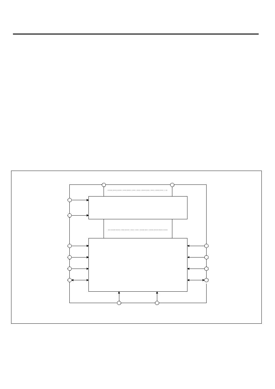
3. BLOCK DIAGRAM
High voltage output and level shifters
Low voltage logic and IO
V
GG
V
EE
V
DD
V
SS
DIO1
OE1
DIO2
FX
RL
X
1
X
240
XDON
OE2
OE3
Fig. 1 Block diagram

EUREKA
EK7308
June 2003
- 3 - Preliminary Rev 0.1
4. PIN FUNCTION DESCRIPTIONS
Table 1. Pad description
Pad Name I/O
Function
DESCRIPTION
X
1
-X
240
O
TFT gate driver
output
Under the control of the shift register data, OE1 or OE2 or OE3, and
DIO1 or DIO2, the driver outputs are V
GG
or V
EE
and change their
value at the rising edge of FX
PATH -
- Short
internally
X
0
, X
241
-
-
LCD panel auxiliary pins. This pins output V
EE
level.
V
EE
- Supply
Negative power supply for Level shifters. Chip ground
V
SS
- Supply
Logic ground, Reference of the voltages
RL I
Shift direction
selection signal
RL = "H" : X
1
to X
240
(Shift left)
RL = "L" : X
240
to X
1
(Shift right)
DIO1 DIO2
RL = "H"
Input
Output
DIO1
DIO2
I/O
Start pulse input
and output
RL = "L"
Output
Input
XDON I
Negative active
input pin
When XDON = "L" then the driver outputs are at the V
GG
level
independence of any other input or register value.
FX I
Shift register clock
input
The start pulse is sampled at the rising edge of FX,
The carry pulse changes at the falling edge of FX.
OE1
OE2
OE3
I
Negative active
input pin
When OE
N
= "H" then the associated outputs are set to V
EE
independent of the register data. This function is not synchronized
with FX.
V
DD
- Supply
Logic positive power
V
GG
- Supply
High voltage power and TFT driver output high level

EUREKA
EK7308
June 2003
- 4 - Preliminary Rev 0.1
5.
FUNCTIONAL OPERATIONS
Power supplies
The TFT voltage is relative to the logic ground, it can be a negative voltage value.
V
GG
V
DD
V
SS
V
EE
Fig. 2 Relative position of the different supply voltages
Shift direction
The input signals OE1, 2, 3 and the shift data control the value of the outputs (X
1
till X
240
). Their value can be either V
GG
or
V
EE
.
The signal LR controls the shift direction of the shift register. The shift register takes its value from one of the input/output
pins DIO at the rising edge of the clock FX and shifts the value to the other input/output pin DIO where it is presented at the
falling edge of FX.
Table 2. RL shift direction relation
RL
Start pulse taken from:
Data shift direction
Output pulse given at:
RL="H" DIO1 X
1
X
240
DIO2
RL="L" DIO2 X
240
X
1
DIO1

EUREKA
EK7308
June 2003
- 5 - Preliminary Rev 0.1
OE function
When the OE1, OE2, OE3 inputs are "H" than the outputs are driven to V
EE
regardless of the contents of the shift register.
Each of the three inputs drives it own set of outputs. This function is not synchronized with FX. The signal XDON can
override this function. In the Table below the relation between each OE1,2,3 and their related outputs is given.
Table 3. OE1,2,3 to Output relation
Signal input
Symbol
LCD driver outputs
OE1 X(3i+1)
i
=0~79
X
1
,X
4
,X
7
,X
10
,...............................................................,X
231
,X
232
,X
235
,X
238
OE2 X(3i+2)
i
=0~79
X
2
,X
5
,X
8
,X
11
, .............................................................................., X
239
OE3 X(3i+3)
i
=0~79
X
3
,X
6
,X
9
,X
12
, ..................................................................,X
234
,X
237
,X
240
1
2
3
4
5
238
239
240
241
FX
DIO1
OE1
X1
X240
DIO2
X2
X3
X4
OE2
OE3
Fig. 3 OE Functionality RL="H"

EUREKA
EK7308
June 2003
- 6 - Preliminary Rev 0.1
1
2
3
4
5
238
239
240
241
FX
DIO2
OE1
X240
X1
DIO1
X239
X238
X237
OE2
OE3
Fig. 4 OE Functionality RL= "L"

EUREKA
EK7308
June 2003
- 7 - Preliminary Rev 0.1
XDON function
When XDON input is "L" then all outputs are driven to the V
GG
level. This function is overriding all other inputs. With this
input all TFT gates are set to high to enable a display off function. This function is not synchronized with FX.
1
2
3
4
5
238
239
240
241
FX
DIO1
OE1
X1
X240
DIO2
X2
X3
X4
OE2
OE3
XDON
Fig. 5 XDON Functionality RL="H"

EUREKA
EK7308
June 2003
- 8 - Preliminary Rev 0.1
PRECAUTIONS
Precaution when connecting or disconnecting the power supply
This IC has a high-voltage LCD driver, so it may be permanently damaged by a high current which may flow, if voltage is
supplied to the LCD driver power supply while the logic system power supply is floating. The detail is as follows.
When connecting the power supply, connect the LCD drive power after connecting the logic system power.
Furthermore, when disconnecting the power, disconnect the logic system power after disconnecting the LCD drive
power.
Voltage
Time
V
SS
V
EE
V
DD
V
GG
Fig. 9
Power ON/OFF sequence

EUREKA
EK7308
June 2003
- 9 - Preliminary Rev 0.1
6. ABSOLUTE MAXIMUM RATINGS
Table 4. Absolute Maximum Ratings
In accordance with the Absolute Maximum Ratings System (IEC 134); See notes 1 and 2
Parameter Symbol Applicable
Pins
Ratings
Unit NOTE
Supply voltage(1)
V
DD
V
DD
V
SS
-0.3 to +7.0
V
V
GG
V
GG
-0.3
to
+45.0
V
Supply voltage(2)
V
EE
V
EE
V
GG
-45 to +0.3
V
Input voltage
V
I
EO1, EO2, EO3, DIO1
DIO2, RL, FX, XDON
V
SS
-0.3 to V
DD
+0.3
V
Storage
temperature
T
stg
-45
to
+125
1, 2
Notes:
1. Stress above those listed under Absolute Maximum Ratings may cause permanent damage to the device
2. Parameters are valid over operating temperature range unless otherwise specified.
RECOMMENDED OPERATING CONDITIONS
Table 5. Recommended operating conditions
Parameter
Symbol Applicable
pins Min. Typ. Max. Unit Notes
Supply voltage(1)
V
DD
V
DD
+2.7
+5.5
V
Supply voltage(2)
V
GG
V
GG
+7.0
+25
V
Supply voltage(3)
V
EE
V
EE
-16
-5
V
1, 2
Operating temperature
T
OPR
-20
+75
Notes:
1. All voltages are with respect to V
SS
unless otherwise noted (0 V).
2. Ensure that voltages are set such that V
EE
V
SS
< V
DD
< V
GG
.

EUREKA
EK7308
June 2003
- 10 - Preliminary Rev 0.1
7.
ELECTRICAL CHARACTERISTICS
Table 6. DC Characteristics
(V
SS
=0 V, V
DD
=+2.5V to +5.5V, V
GG
=+15.0 to +40.0 V, T
OPR
=-25)
Parameter Symbol Conditions
Applicable
pins
Min. Typ. Max. Unit Note
IDD V
DD
800
A
Operating Supply Current
IGG
fFX=15.7kHz
V
DD
=3.3V
V
EE
=-15V
V
GG
=15V
Output with no load
V
GG
300
A
IDS V
DD
600
A
Standby
Quiescent
Supply Current
IGS
Standby
V
DD
=3.3V
V
EE
=-15V
V
GG
=15V
V
GG
100
A
Input pin
H input voltage
VIH1
0.7x V
DD
V
DD
V
L input voltage
VIL1
0
0.3x
V
DD
V
Input leakage current
VLI1
RL,FX,
OE1~3,
-1 1 A
XDON
except
Output pin
H input voltage
VIH3
0.7x V
DD
V
DD
V
L input voltage
VIL3
0.3x V
DD
V
H output voltage
VOH
I
O
= -100 A V
DD
-0.4
V
L output voltage
VOL
I
O
= 100 A
DIO1,
DIO2
0.4
V
Liquid crystal driving output pin
Output leakage current
VLO1
-50
50
A
RON-
V
GG
V
GG
=15V
V
EE
=-15V
V
OM
=VGG-0.5V
V
OM
is X
1
~X
240
600 1000
Output ON resistance
RON-
V
EE
V
GG
=15V
V
EE
=-15V
V
OM
=V
EE
+0.5V
V
OM
is X
1
~X
240
X
1
~X
240
600 1000

EUREKA
EK7308
June 2003
- 11 - Preliminary Rev 0.1
Table 7.
AC Characteristics
(V
SS
= 0 V, V
DD
=+2.5V to +5.5V, V
GG
-V
EE
=+30.0 to +40.0 V, T
OPR
=25)
Parameter Symbol
Conditions
Min.
Typ.
Max.
Unit
Clock period
t
FX
-
200
KHz
In cascade
connection
Pulse width of clock H level
t
WH
500
ns
Pulse width of clock L level
t
WL
500
ns
DIO data set up time
t
su
200
ns
DIO data hold time
t
h
300
ns
DIO output delay time
t
pd1
CL=20pF
500 ns
Xn output delay time
t
pd2
CL=220pF
10 us
Input Rise Time
t
r
100
ns
Input Fall Time
t
f
100
ns
OEX output delay time
t
pd3
CL=220pF
900 ns
Timing Chart
FX
t
WL
DIO Input
DIO Output
20%
20%
80%
80%
50%
20%
t
FX
50%
80%
80%
t
su
t
h
60%
40%
t
pd1
t
pd1
60%
40%
t
pd2
Xn
Xn
OEm
80%
60%
t
pd3
20%
40%
t
WH
90%
90%
10%
t
r
t
f
XDON
Xn
60%
20%
t
pd2
t
pd2
80%
40%
10%
t
pd3
Fig. 10 Timing

EUREKA
EK7308
June 2003
- 12 - Preliminary Rev 0.1
8.
DEFINITIONS
Data Sheet status
Objective specification
This data sheet contains target or goal specification for product development.
Preliminary specification This data sheet contains preliminary data; supplementary data may be published later.
Product specification
This data sheet contains final product specification.
Application information
Where application information is given, it is advisory and does not form part of the specification.
LIFE SUPPORT APPLICATIONS
These products are not designed for use in life support appliances, devices, or systems where malfunction of these
products can reasonably be expected to result in personal injury. Eureka customers using or selling these products for use
in such applications do so at their own risk and agree to fully indemnify Eureka for any damages resulting from such
improper use or sale.