
CMT2N7002
S
MALL
S
IGNAL
MOSFET
GENERAL DESCRIPTION
FEATURES
This N-Channel enhancement mode field effect transistor is
produced using high cell density, DMOS technology. These
products have been designed to minimize on-state
resistance while provide rugged, reliable, and fast switching
performance. It can be used in most applications requiring
up to 115mA DC and can deliver pulsed currents up to
800mA. This product is particularly suited for low voltage,
low current applications such as small servo motor control,
power MOSFET gate drivers, and other switching
applications.
High Density Cell Design for Low R
DS(ON)
Voltage Controlled Small Signal Switch
Rugged and Reliable
High Saturation Current Capability
PIN CONFIGURATION
SYMBOL
SOT-23
Top View
1
3
2
GA
T
E
DRAI
N
SO
URCE
D
S
G
N-Channel MOSFET
ORDERING INFORMATION
Part Number
Package
CMT2N7002 SOT-23
CMT2N7002G* SOT-23
*Note:
G : Suffix for Pb Free Product
ABSOLUTE MAXIMUM RATINGS
Rating Symbol
Value
Unit
Drain Source Voltage
V
DSS
60 V
Drain-Gate Voltage (R
GS
= 1.0M) V
DGR
60 V
Drain to Current Continuous
Pulsed
I
D
I
DM
�115
�800
mA
Gate-to-Source Voltage Continue
Non-repetitive
V
GS
V
GSM
�20
�40
V
V
Total Power Dissipation
Derate above 25
P
D
225
1.8
mW
mW/
Single Pulse Drain-to-Source Avalanche Energy T
J
= 25
(V
DD
= 50V, V
GS
= 10V, I
AS
= 0.8A, L = 30mH, R
G
= 25)
E
AS
9.6 mJ
Operating and Storage Temperature Range
T
J
, T
STG
-55 to 150
Thermal Resistance Junction to Ambient
JA
417
/W
Maximum Lead Temperature for Soldering Purposes, 1/8" from case for 10 seconds
T
L
300
Formosa MS
CMT2N7002
S
MALL
S
IGNAL
MOSFET
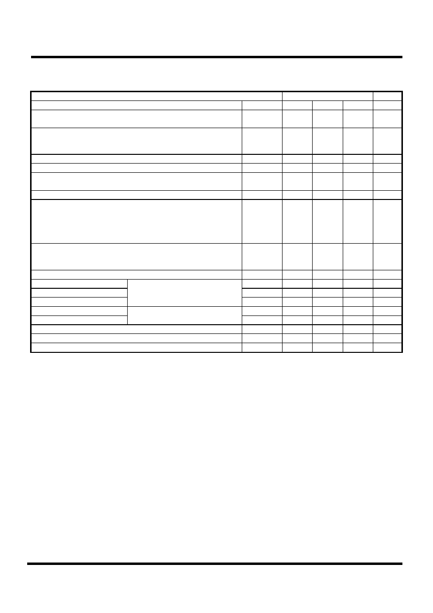
ELECTRICAL CHARACTERISTICS
Unless otherwise specified, T
J
= 25.
CMT2N7002
Characteristic Symbol
Min
Typ
Max
Units
Drain-Source Breakdown Voltage
(V
GS
= 0 V, I
D
= 10 A)
V
(BR)DSS
60
V
Drain-Source Leakage Current
(V
DS
= 60 V, V
GS
= 0 V)
(V
DS
= 60 V, V
GS
= 0 V, T
J
= 125)
I
DSS
1.0
0.5
A
mA
Gate-Source Leakage Current-Forward (V
gsf
= 20 V)
I
GSSF
100
nA
Gate-Source Leakage Current-Reverse (V
gsf
= -20 V)
I
GSSF
-100
nA
Gate Threshold Voltage *
(V
DS
= V
GS
, I
D
= 250 A)
V
GS(th)
1.0 2.5 V
On-State Drain Current (V
DS
2.0 V
DS(on)
, V
GS
= 10V)
I
d(on)
500 mA
Static Drain-Source On-Resistance *
(V
GS
= 10 V, I
D
= 0.5A)
(V
GS
= 10 V, I
D
= 0.5A, T
C
= 125)
(V
GS
= 5.0 V, I
D
= 50mA)
(V
GS
= 5.0 V, I
D
= 50mA, T
C
= 125)
R
DS(on)
7.5
13.5
7.5
13.5
Drain-Source On-Voltage *
(V
GS
= 10 V, I
D
= 0.5A)
(V
GS
= 5.0 V, I
D
= 50mA)
V
DS(on)
3.75
0.375
V
Forward Transconductance (V
DS
2.0 V
DS(on)
, I
D
= 200mA) *
g
FS
80
mmhos
Input Capacitance
C
iss
50
pF
Output Capacitance
C
oss
25
pF
Reverse Transfer Capacitance
(V
DS
= 25 V, V
GS
= 0 V,
f = 1.0 MHz)
C
rss
5.0
pF
Turn-On Delay Time
t
d(on)
20
ns
Turn-Off Delay Time
(V
DD
= 25 V, I
D
= 500 mA,
V
gen
= 10 V, R
G
= 25, R
L
= 50) *
t
d(off)
40
ns
Diode Forward On-Voltage (IS = 115 mA, VGS = 0V)
V
SD
-1.5
V
Source Current Continuous (Body Diode)
I
S
-115
mA
Source Current Pulsed
I
SM
-800
mA
* Pulse Test: Pulse Width 300�s, Duty Cycle 2%
Formosa MS

