 | –≠–ª–µ–∫—Ç—Ä–æ–Ω–Ω—ã–π –∫–æ–º–ø–æ–Ω–µ–Ω—Ç: 100B8R2CW | –°–∫–∞—á–∞—Ç—å:  PDF PDF  ZIP ZIP |

MW4IC2230NBR1 MW4IC2230GNBR1
1
RF Device Data
Freescale Semiconductor
RF LDMOS Wideband Integrated
Power Amplifiers
The MW4IC2230N wideband integrated circuit is designed for W-CDMA
base station applications. It uses Freescale's newest High Voltage (26 to 28
Volts) LDMOS IC technology and integrates a multi - stage structure. Its
wideband on-chip design makes it usable from 1600 to 2400 MHz. The linearity
performances cover all modulations for cellular applications: GSM, GSM
EDGE, TDMA, CDMA and W-CDMA.
Final Application
∑ Typical Single-Carrier W-CDMA Performance:
V
DD
= 28 Volts, I
DQ1
=
60 mA, I
DQ2
= 350 mA, P
out
= 5 Watts Avg., f = 2140 MHz, Channel
Bandwidth = 3.84 MHz, PAR = 8.5 dB @ 0.01% Probability on CCDF.
Power Gain -- 31 dB
Drain Efficiency -- 15%
ACPR @ 5 MHz = -45 dBc in 3.84 MHz Bandwidth
Driver Application
∑ Typical Single-Carrier W-CDMA Performance:
V
DD
= 28 Volts, I
DQ1
=
60 mA, I
DQ2
= 350 mA, P
out
= 0.4 Watts Avg., f = 2140 MHz, Channel
Bandwidth = 3.84 MHz, PAR = 8.5 dB @ 0.01% Probability on CCDF.
Power Gain -- 31.5 dB
ACPR @ 5 MHz = -53.5 dBc in 3.84 MHz Bandwidth
∑ Capable of Handling 3:1 VSWR, @ 28 Vdc, 2170 MHz, 5 Watts CW
Output Power
∑ Stable into a 3:1 VSWR. All Spurs Below -60 dBc @ 10 mW to 5 W CW
P
out
.
Features
∑ Characterized with Series Equivalent Large-Signal Impedance Parameters
∑ On-Chip Matching (50 Ohm Input, DC Blocked, >5 Ohm Output)
∑ Integrated Quiescent Current Temperature Compensation
with Enable/Disable Function
∑ On-Chip Current Mirror g
m
Reference FET for Self Biasing Application
(1)
∑ Integrated ESD Protection
∑ 200∞C Capable Plastic Package
∑ N Suffix Indicates Lead-Free Terminations. RoHS Compliant.
∑ In Tape and Reel. R1 Suffix = 500 Units per 44 mm, 13 inch Reel
Figure 1. Functional Block Diagram
Figure 2. Pin Connections
(Top View)
GND
V
DS1
RF
in
V
GS1
GND
V
DS2
V
DS3/
RF
out
GND
V
GS2
V
GS3
GND
Quiescent Current
Temperature Compensation
3 Stages I
C
V
GS1
RF
in
V
DS2
V
DS1
V
GS2
V
GS3
2
3
4
5
6
7
8
16
15
14
13
12
9
10
11
V
DS3
/RF
out
1
Note: Exposed backside flag is source
terminal for transistors.
V
RD1
V
RG1
V
RD1
V
RG1
1. Refer to AN1987, Quiescent Current Control for the RF Integrated Circuit Device Family. Go to http://www.freescale.com/rf.
Select Documentation/Application Notes - AN1987.
Document Number: MW4IC2230N
Rev. 6, 5/2006
Freescale Semiconductor
Technical Data
2110-2170 MHz, 30 W, 28 V
SINGLE W-CDMA
RF LDMOS WIDEBAND
INTEGRATED POWER AMPLIFIERS
CASE 1329-09
TO-272 WB-16
PLASTIC
MW4IC2230NBR1
MW4IC2230NBR1
MW4IC2230GNBR1
CASE 1329A-03
TO-272 WB-16 GULL
PLASTIC
MW4IC2230GNBR1
© Freescale Semiconductor, Inc., 2006. All rights reserved.
2
RF Device Data
Freescale Semiconductor
MW4IC2230NBR1 MW4IC2230GNBR1
Table 1. Maximum Ratings
Rating
Symbol
Value
Unit
Drain-Source Voltage
V
DSS
-0.5, +65
Vdc
Gate-Source Voltage
V
GS
-0.5, +8
Vdc
Storage Temperature Range
T
stg
-65 to +175
∞C
Operating Channel Temperature
T
J
200
∞C
Input Power
P
in
20
dBm
Table 2. Thermal Characteristics
Characteristic
Symbol
Value
(1)
Unit
Thermal Resistance, Junction to Case
Stage 1
Stage 2
Stage 3
R
JC
10.5
5.1
2.3
∞C/W
Table 3. ESD Protection Characteristics
Test Conditions
Class
Human Body Model
2 (Minimum)
Machine Model
M3 (Minimum)
Charge Device Model
C5 (Minimum)
Table 4. Moisture Sensitivity Level
Test Methodology
Rating
Package Peak Temperature
Unit
Per JESD 22-A113, IPC/JEDEC J-STD-020
3
260
∞C
Table 5. Electrical Characteristics
(T
C
= 25∞C unless otherwise noted)
Characteristic
Symbol
Min
Typ
Max
Unit
Functional Tests (In Freescale Test Fixture, 50 ohm system) V
DD
= 28 Vdc, I
DQ1
= 60 mA, I
DQ2
= 350 mA, I
DQ3
= 265 mA,
P
out
= 0.4 W Avg., f = 2110 MHz, f = 2170 MHz, Single-carrier W-CDMA. ACPR measured in 3.84 MHz Channel Bandwidth @ ±5 MHz
Offset. PAR = 8.5 dB @ 0.01% Probability on CCDF.
Power Gain
G
ps
29
31.5
--
dB
Input Return Loss
IRL
--
-25
-10
dB
Adjacent Channel Power Ratio
P
out
= 0.4 W Avg.
P
out
= 1.26 W Avg.
ACPR
--
--
-53.5
-52
-50
--
dBc
Typical Performances (In Freescale Test Fixture tuned for 0.4 W Avg. W-CDMA driver) V
DD
= 28 Vdc, I
DQ1
= 60 mA, I
DQ2
= 350 mA,
I
DQ3
= 265 mA, 2110 MHz<Frequency <2170 MHz
Saturated Pulsed Output Power
(f = 1 kHz, Duty Cycle 10%)
P
sat
--
43
--
W
Quiescent Current Accuracy over Temperature (-10 to 85∞C)
(2)
I
QT
--
±5
--
%
Gain Flatness in 30 MHz Bandwidth
G
F
--
0.13
--
dB
Deviation from Linear Phase in 30 MHz Bandwidth
--
±1
--
∞
Delay @ P
out
= 0.4 W CW Including Output Matching
Delay
--
1.6
--
ns
Part-to-Part Phase Variation
--
±15
--
∞
1. Refer to AN1955, Thermal Measurement Methodology of RF Power Amplifiers. Go to http://www.freescale.com/rf.
Select Documentation/Application Notes - AN1955.
2. Refer to AN1977, Quiescent Current Thermal Tracking Circuit in the RF Integrated Circuit Family. Go to http://www.freescale.com/rf. Select
Documentation/Application Notes - AN1977.
(continued)

MW4IC2230NBR1 MW4IC2230GNBR1
3
RF Device Data
Freescale Semiconductor
Table 5. Electrical Characteristics
(T
C
= 25∞C unless otherwise noted)
(continued)
Characteristic
Symbol
Min
Typ
Max
Unit
Typical Performances (In Freescale Reference Application Circuit tuned for 2-carrier W-CDMA signal) V
DD
= 28 Vdc,
P
out
= 0.4 W Avg., I
DQ1
= 60 mA, I
DQ2
= 400 mA, I
DQ3
= 245 mA, f1 = 2112.5 MHz, f2 = 2122.5 MHz and f1 = 2157.5 MHz, f2 = 2167.5 MHz,
2-carrier W-CDMA, 3.84 MHz Channel Bandwidth Carriers. ACPR measured in 3.84 MHz Channel Bandwidth @ ±5 MHz Offset. IM3
measured in 3.84 MHz Channel Bandwidth @ ±10 MHz Offset. PAR = 8.5 dB @ 0.01% Probability on CCDF.
Power Gain
G
ps
--
31.5
--
dB
Intermodulation Distortion
IM3
--
-52
--
dBc
Adjacent Channel Power Ratio
ACPR
--
-55
--
dBc
Input Return Loss
IRL
--
-26
--
dB
4
RF Device Data
Freescale Semiconductor
MW4IC2230NBR1 MW4IC2230GNBR1
Z6
1.120 x 0.090 Microstrip
Z7
0.340 x 0.090 Microstrip
PCB
Taconic TLX8-0300, 0.030,
r
= 2.55
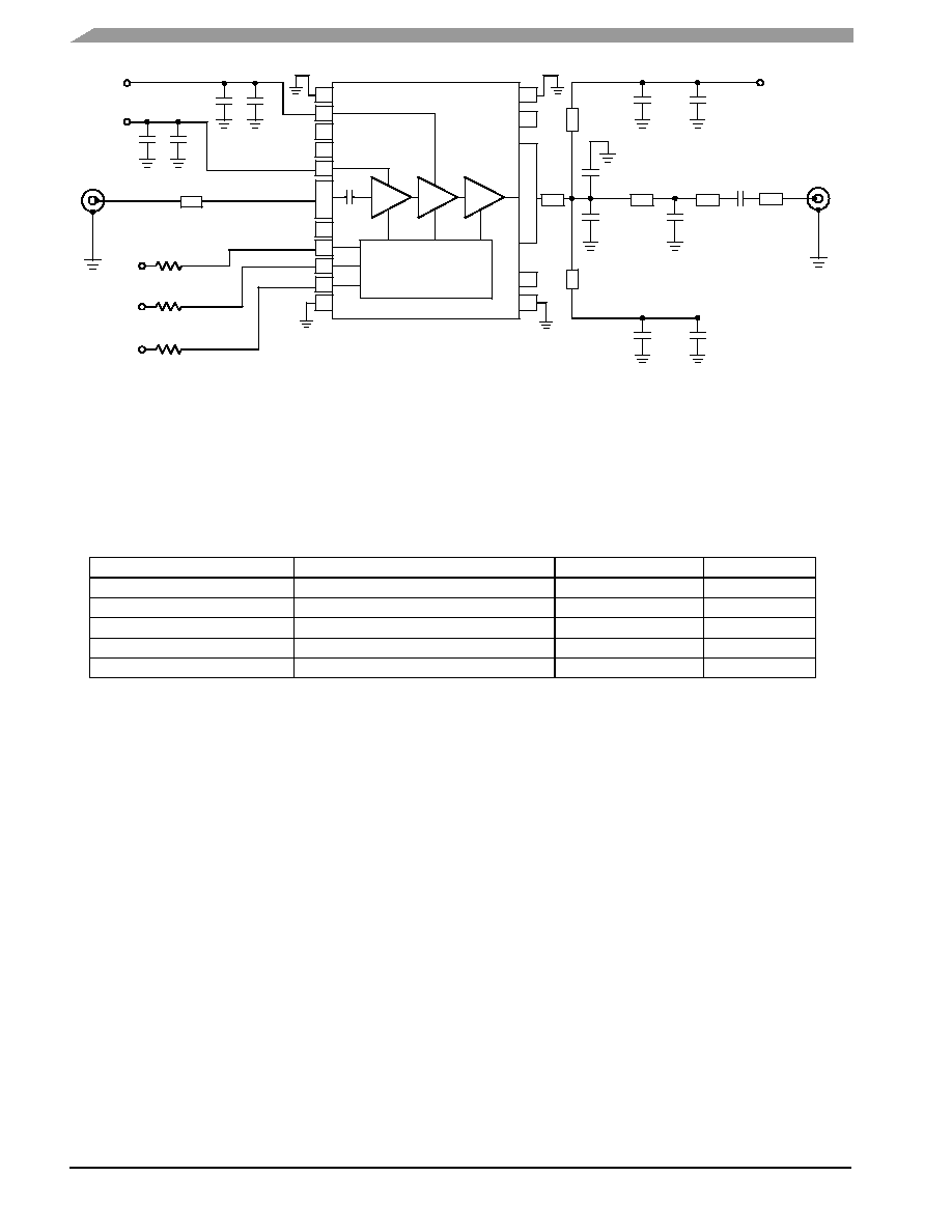
Figure 3. MW4IC2230NBR1(GNBR1) Test Circuit Schematic
Z1
2.180 x 0.090 Microstrip
Z2, Z3
0.040 x 0.430 Microstrip
Z4
0.350 x 0.240 Microstrip
Z5
0.420 x 0.090 Microstrip
C6
C1
R1
R2
Z1
RF
INPUT
V
D1
V
G1
V
G2
Z4
Z5
Z7
RF
OUTPUT
C12
C7
C3
+
V
D3
1
2
3
4
5
6
7
8
14
13
12
11
10
9
15
16
NC
NC
NC
NC
NC
Z6
DUT
C9
C10
C11
+
R3
V
G3
C5
C2
V
D2
+
Z2
C8
C4
+
Z3
Quiescent Current
Temperature Compensation
Table 6. MW4IC2230NBR1(GNBR1) Test Circuit Component Designations and Values
Part
Description
Part Number
Manufacturer
C1, C2, C3, C4
10 F, 35 V Tantalum Capacitors
TAJD106K035
AVX
C5, C6, C7, C8, C12
8.2 pF 100B Chip Capacitors
100B8R2CW
ATC
C9, C10
1.8 pF 100B Chip Capacitors
100B1R8BW
ATC
C11
0.3 pF 100B Chip Capacitor
100B0R3BW
ATC
R1, R2, R3
1.8 kW Chip Resistors (1206)
MW4IC2230NBR1 MW4IC2230GNBR1
5
RF Device Data
Freescale Semiconductor
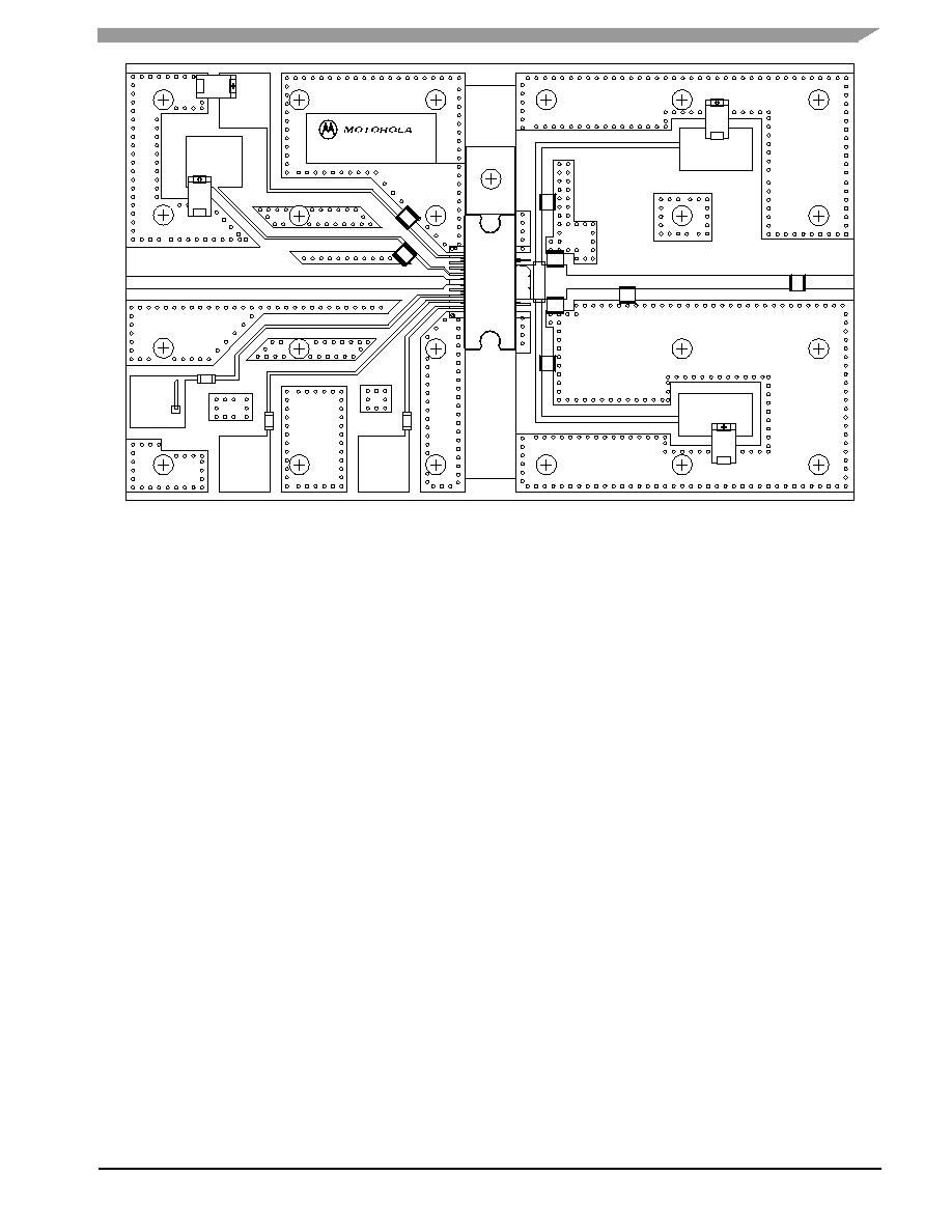
Figure 4. MW4IC2230NBR1(GNBR1) Test Circuit Component Layout
R1
V
G1
C6
V
G2
V
D1
V
G3
V
D2
GND
C2
C1
R2
R3
C4
Rev 1
MW4IC2230
V
D3
C7
C5
C8
C9
C10
C11
C12
C3
Freescale has begun the transition of marking Printed Circuit Boards (PCBs) with the Freescale Semiconductor
signature/logo. PCBs may have either Motorola or Freescale markings during the transition period. These changes will have
no impact on form, fit or function of the current product.