
56F8014 Technical Data, Rev. 3
2
Freescale Semiconductor
Preliminary
Document Revision History
Version History
Description of Change
Rev 0
Initial release
Rev 1
Updates to
Part 10, Specifications,
Table 10-1
, added maximum clamp current , per pin
Table 10-11
, clarified variation over temperature table and graph
Table 10-15
, added LIN slave timing
Rev 2
Added alternate pins to
Figure 11-1
and
Table 11-1
.
Rev 3
Corrected bit selects in Timer Channel 3 Input (TC3_INP) bit 9 ,
Section 6.3.1.7
, clarified
Section 1.4.1
, and simplified notes in
Table 10-9
,
Please see http://www.freescale.com for the most current Data Sheet revision.
56F8014 Technical Data, Rev. 3
Freescale Semiconductor
3
Preliminary
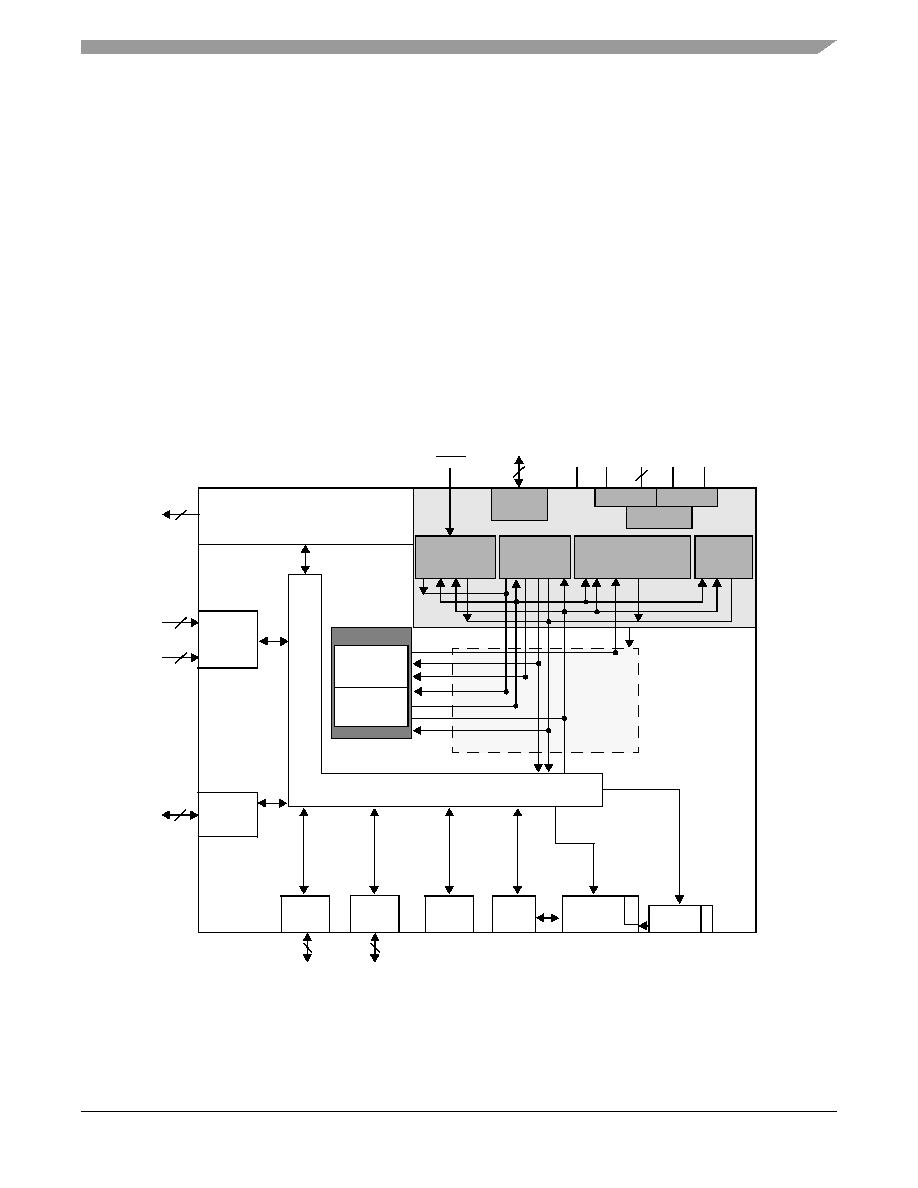
56F8014 Block Diagram
Program Controller
and Hardware
Looping Unit
Data ALU
16 x 16 + 36 -> 36-Bit MAC
Three 16-bit Input Registers
Four 36-bit Accumulators
Address
Generation Unit
Bit
Manipulation
Unit
16-Bit
56800E Core
Interrupt
Controller
4
Unified Data /
Program RAM
4KB
PDB
PDB
XAB1
XAB2
XDB2
CDBR
SPI or I
2
C
or Timer
or GPIOB
IPBus Bridge (IPBB)
System Bus
Control
R/W Control
Memory
PAB
PAB
CDBW
CDBR
CDBW
JTAG/EOnCE
Port or
GPIOD
Digital Reg
Analog Reg
Low-Voltage
Supervisor
V
CAP
V
DD
V
SS_IO
V
DDA
V
SSA
4
RESET
5
Timer or
GPIOB
AD0
2
4
Clock
Generator*
System
Integration
Module
P
O
R
O
S
C
PWM Outputs
PWM
or Timer Port
or GPIOA
*Includes On-Chip
Relaxation Oscillator
COP/
Watchdog
AD1
4
Program Memory
8K x 16 Flash
ADC
or
GPIOC
SCI
or I
2
C
or GPIOB
2
2
∑ Up to 32 MIPS at 32MHz core frequency
∑ DSP and MCU functionality in a unified,
C-efficient architecture
∑ 16KB Program Flash
∑ 4KB Unified Data/Program RAM
∑ One 5-channel PWM module
∑ Two 4-channel 12-bit ADCs
∑ One Serial Communication Interface (SCI) with LIN
slave functionality
∑ One Serial Peripheral Interface (SPI)
∑ One 16-bit Quad Timer
∑ One Inter-Integrated Circuit (I
2
C) Port
∑ Computer Operating Properly (COP)/Watchdog
∑ On-Chip Relaxation Oscillator
∑ Integrated Power-On Reset and Low-Voltage Interrupt
Module
∑ JTAG/Enhanced On-Chip Emulation (OnCETM) for
unobtrusive, real-time debugging
∑ Up to 26 GPIO lines
∑ 32-pin LQFP Package
56F8014 General Description

56F8014 Technical Data, Rev. 3
4
Freescale Semiconductor
Preliminary
Part 1: Overview . . . . . . . . . . . . . . . . . . . . . . 5
1.1. 56F8014 Features . . . . . . . . . . . . . . . . . . . . 5
1.2. 56F8014 Description . . . . . . . . . . . . . . . . . . . 6
1.3. Award-Winning Development Environment . . 7
1.4. Architecture Block Diagram . . . . . . . . . . . . . . 7
1.5. Product Documentation . . . . . . . . . . . . . . . . 11
1.6. Data Sheet Conventions. . . . . . . . . . . . . . . . 11
Part 2: Signal/Connection Descriptions . . . 12
2.1. Introduction . . . . . . . . . . . . . . . . . . . . . . . . . 12
2.2. 56F8014 Signal Pins . . . . . . . . . . . . . . . . . . 15
Part 3: OCCS . . . . . . . . . . . . . . . . . . . . . . . . . 24
3.1. Overview . . . . . . . . . . . . . . . . . . . . . . . . . . . 24
3.2. Features . . . . . . . . . . . . . . . . . . . . . . . . . . . 24
3.3. Operating Modes . . . . . . . . . . . . . . . . . . . . 24
3.4. Block Diagram . . . . . . . . . . . . . . . . . . . . . . . 26
3.5. Pin Descriptions . . . . . . . . . . . . . . . . . . . . . . 27
Part 4: Memory Map . . . . . . . . . . . . . . . . . . . 27
4.1. Introduction . . . . . . . . . . . . . . . . . . . . . . . . . 27
4.2. Interrupt Vector Table . . . . . . . . . . . . . . . . . 27
4.3. Program Map . . . . . . . . . . . . . . . . . . . . . . . . 29
4.4. Data Map . . . . . . . . . . . . . . . . . . . . . . . . . . 30
4.5. EOnCE Memory Map . . . . . . . . . . . . . . . . . 31
4.6. Peripheral Memory Mapped Registers . . . . 32
Part 5: Interrupt Controller (ITCN) . . . . . . . . 42
5.1. Introduction . . . . . . . . . . . . . . . . . . . . . . . . . 42
5.2. Features . . . . . . . . . . . . . . . . . . . . . . . . . . . 42
5.3. Functional Description . . . . . . . . . . . . . . . . 42
5.4. Block Diagram . . . . . . . . . . . . . . . . . . . . . . . 44
5.5. Operating Modes . . . . . . . . . . . . . . . . . . . . . 44
5.6. Register Descriptions . . . . . . . . . . . . . . . . . . 45
5.7. Resets . . . . . . . . . . . . . . . . . . . . . . . . . . . . . 61
Part 6: System Integration Module (SIM) . . 62
6.1. Introduction . . . . . . . . . . . . . . . . . . . . . . . . . 62
6.2. Features . . . . . . . . . . . . . . . . . . . . . . . . . . . 62
6.3. Register Descriptions . . . . . . . . . . . . . . . . . . 63
6.4. Clock Generation Overview . . . . . . . . . . . . 76
6.5. Power-Down Modes . . . . . . . . . . . . . . . . . . 77
6.6. Resets . . . . . . . . . . . . . . . . . . . . . . . . . . . . . 78
6.7. Clocks . . . . . . . . . . . . . . . . . . . . . . . . . . . . . 80
6.8. Interrupts . . . . . . . . . . . . . . . . . . . . . . . . . . . 81
Part 7: Security Features. . . . . . . . . . . . . . . 82
7.1. Operation with Security Enabled . . . . . . . . . 82
7.2. Flash Access Lock and Unlock Mechanisms 82
Part 8: General Purpose Input/Output
(GPIO) . . . . . . . . . . . . . . . . . . . . . . . . . . . . . . .84
8.1. Introduction . . . . . . . . . . . . . . . . . . . . . . . . . 84
8.2. Configuration . . . . . . . . . . . . . . . . . . . . . . . . 84
8.3. Reset Values . . . . . . . . . . . . . . . . . . . . . . . . 86
Part 9: Joint Test Action Group (JTAG) . . .91
9.1. 56F8014 Information . . . . . . . . . . . . . . . . . . 91
Part 10: Specifications . . . . . . . . . . . . . . . . .91
10.1. General Characteristics . . . . . . . . . . . . . . . 91
10.2. DC Electrical Characteristics . . . . . . . . . . . 95
10.3. AC Electrical Characteristics . . . . . . . . . . . 98
10.4. Flash Memory Characteristics . . . . . . . . . . 98
10.5. External Clock Operation Timing . . . . . . . . 99
10.6. Phase Locked Loop Timing . . . . . . . . . . . . 99
10.7. Relaxation Oscillator Timing. . . . . . . . . . . 100
10.8. Reset, Stop, Wait, Mode Select, and Interrupt
Timing . . . . . . . . . . . . . . . . . . . . . 101
10.9. Serial Peripheral Interface (SPI) Timing . 102
10.10. Quad Timer Timing . . . . . . . . . . . . . . . . 105
10.11. Serial Communication Interface
(SCI) Timing . . . . . . . . . . . . . . . . 106
10.12. Inter-Integrated Circuit Interface
(I2C) Timing . . . . . . . . . . . . . . . . 107
10.13. JTAG Timing . . . . . . . . . . . . . . . . . . . . . 108
10.14. Analog-to-Digital Converter
(ADC) Parameters 109
10.15. Equivalent Circuit for ADC Inputs . . . . . 110
10.16. Power Consumption . . . . . . . . . . . . . . . 111
Part 11: Packaging . . . . . . . . . . . . . . . . . . .113
11.1. 56F8014 Package and Pin-Out Information 113
Part 12: Design Considerations . . . . . . . . .116
12.1. Thermal Design Considerations . . . . . . . 116
12.2. Electrical Design Considerations . . . . . . . 117
Part 13: Ordering Information . . . . . . . . . .119
Part 14: Appendix . . . . . . . . . . . . . . . . . . . .120
56F8014 Data Sheet Table of Contents

56F8014 Features
56F8014 Technical Data, Rev. 3
Freescale Semiconductor
5
Preliminary
Part 1 Overview
1.1 56F8014 Features
1.1.1
Digital Signal Controller Core
∑
Efficient 16-bit 56800E family Digital Signal Controller (DSC) engine with dual Harvard architecture
∑
As many as 32 Million Instructions Per Second (MIPS) at 32MHz core frequency
∑
Single-cycle 16
◊ 16-bit parallel Multiplier-Accumulator (MAC)
∑
Four 36-bit accumulators, including extension bits
∑
Arithmetic and logic multi-bit shifter
∑
Parallel instruction set with unique DSP addressing modes
∑
Hardware DO and REP loops
∑
Three internal address buses
∑
Four internal data buses
∑
Instruction set supports both DSP and controller functions
∑
Controller-style addressing modes and instructions for compact code
∑
Efficient C compiler and local variable support
∑
Software subroutine and interrupt stack with depth limited only by memory
∑
JTAG/EOnCE debug programming interface
1.1.2
Memory
∑
Harvard architecture permits as many as three simultaneous accesses to program and data memory
∑
Flash security and protection
∑
On-chip memory, including a low-cost, high-volume Flash solution
-- 16KB of Program Flash
-- 4KB of Unified Data/Program RAM
∑
EEPROM emulation capability
1.1.3
Peripheral Circuits for 56F8014
∑
One Pulse Width Modulator (PWM) module with five PWM outputs and three Fault inputs; fault-tolerant
design with dead time insertion; supports both center-aligned and edge-aligned modes
∑
One eight-input, 12-bit, Analog-to-Digital Converter (ADC), which support two simultaneous conversions
with dual, 4-pin multiplexed inputs; ADC and PWM modules can be synchronized through Timer Channels
2 and 3
∑
One 16-bit Quad Timer module (TMR) totaling four pins: Timer works in conjunction with the PWM and
ADC
∑
One Serial Communication Interface (SCI) with LIN Slave functionality
∑
One Serial Peripheral Interface (SPI)
∑
Computer Operating Properly (COP)/Watchdog timer