 | –≠–ª–µ–∫—Ç—Ä–æ–Ω–Ω—ã–π –∫–æ–º–ø–æ–Ω–µ–Ω—Ç: AN2528D | –°–∫–∞—á–∞—Ç—å:  PDF PDF  ZIP ZIP |

© Motorola, Inc., 2003
AN2528/D
Rev. 0, 5/2003
Standard Space Vector
Modulation TPU Function Set
(svmStd)
Application Note
By Milan Brejl, Ph.D.
Functional Overview
Standard Space Vector Modulation (svmStd) is a technique that is used to
implement a straightforward method of switching motor windings in
applications such as AC induction motor control and PMSM motor control. The
function set consists of 5 TPU functions:
∑
Standard Space Vector Modulation ≠ Top (svmStd_top)
∑
Standard Space Vector Modulation ≠ Bottom (svmStd_bottom)
∑
Synchronization Signal for Standard Space Vector Modulation
(svmStd_sync)
∑
Resolver Reference Signal for Standard Space Vector Modulation
(svmStd_res)
∑
Fault Input for Standard Space Vector Modulation (svmStd_fault)
The svmStd_top and svmStd_bottom TPU functions work together to generate
a 6-channel 3-phase center-aligned PWM signal with dead-time between the
top and bottom channels. The Synchronization Signal for the svmStd function
Figure 1. Signals generated by svmStd TPU function set
C hange of
PW M period
F AU LT !
N ew
IN IT IA LIZAT IO N
Phase A - top
Phase A - bottom
Phase B - top
Phase B - bottom
Phase C - top
Phase C - bottom
Fault (input signal)
Synchronization signal
1.6 m s
R esolver reference signal
C hange of
PW M period
F AU LT !
N ew
IN IT IA LIZAT IO N
Phase A - top
Phase A - bottom
Phase B - top
Phase B - bottom
Phase C - top
Phase C - bottom
Fault (input signal)
Synchronization signal
1.6 m s
R esolver reference signal
F
r
e
e
s
c
a
l
e
S
e
m
i
c
o
n
d
u
c
t
o
r
,
I
Freescale Semiconductor, Inc.
For More Information On This Product,
Go to: www.freescale.com
n
c
.
.
.
© Freescale Semiconductor, Inc., 2004. All rights reserved.

AN2528/D
2
Standard Space Vector Modulation TPU Function Set (svmStd)
can be used to generate one or more adjustable signals for a wide range of
uses, that are synchronized to the PWM, and track changes in the PWM period.
The Resolver Reference Signal for the svmStd function can be used to
generate one or more 50% duty-cycle adjustable signals that are also
synchronized to the PWM.The Fault Input for the svmStd function is a TPU
input function that sets all PWM outputs low when the input signal goes low.
See
Figure 1
.
Function Set Configuration
None of the TPU functions in the Standard Space Vector Modulation TPU
function set can be used separately. The svmStd_top and svmStd_bottom
functions have to be used together. The svmStd_top is used on 3 channels, the
svmStd_bottom on a further 3 channels, and within each phase, the function
svmStd_top has to be assigned on a lower TPU channel than the function
svmStd_bottom. This is illustrated in the examples in
Table 2
and
Table 3
. One
or more channels running a Synchronization Signal for svmStd as well as
Resolver Reference Signals for svmStd functions can be added to the
svmStd_top and svmStd_bottom functions. They can run with different settings
on each channel. The function Fault Input for svmStd can also be added to the
svmStd_top and svmStd_bottom functions. It is recommended to use it on
channel 15, and to select the hardware option that disables all TPU output pins
when the channel 15 input signal is low (DTPU bit = 1). This ensures that the
hardware reacts quickly to a pin fault state. Note that it is not only the PWM
channels, but all TPU output channels, including the synchronization signals,
that are disabled in this configuration.
Table 1
shows the configuration options and restrictions.
Table 2
and
Table 3
show two examples of configuration.
Table 1. svmStd TPU function set configuration options and restrictions
TPU function
Optional/
Mandatory
How many
channels
Assignable channels
svmStd_top
mandatory
3
any 3 channels, within each phase a
lower TPU channel than the same
phase svmStd_bottom
svmStd_bottom
mandatory
3
any 3 channels, within each phase a
higher TPU channel than the same
phase svmStd_top
svmStd_sync
optional
1 or more
any channels
svmStd_res
optional
1 or more
any channels
svmStd_fault
optional
1
any, recommended is 15 and DTPU bit
set
F
r
e
e
s
c
a
l
e
S
e
m
i
c
o
n
d
u
c
t
o
r
,
I
Freescale Semiconductor, Inc.
For More Information On This Product,
Go to: www.freescale.com
n
c
.
.
.

AN2528/D
Function Set Configuration
Standard Space Vector Modulation TPU Function Set (svmStd)
3
Table 4
shows the TPU function code sizes.
Configuration Order
The CPU configures the TPU as follows.
1.
Disables the channels by clearing the two channel priority bits on each
channel used (not necessary after reset).
2.
Selects the channel functions on all used channels by writing the
function numbers to the channel function select bits.
Table 2. Example of configuration
Channel
TPU function
Priority
0
svmStd_top
high
1
svmStd_bottom
high
2
svmStd_top
high
3
svmStd_bottom
high
4
svmStd_top
high
5
svmStd_bottom
high
10
svmStd_sync
low
15
svmStd_fault
high
Table 3. Example of configuration
Channel
TPU function
Priority
0
svmStd_top
high
1
svmStd_top
high
2
svmStd_top
high
3
svmStd_bottom
high
4
svmStd_bottom
high
5
svmStd_bottom
high
10
svmStd_sync
low
11
svmStd_res
low
15
svmStd_fault
high
Table 4. TPU function code sizes
TPU function
Code size
svmStd_top
16
µ
instructions + 8 entries = 24 long words
svmStd_bottom
197
µ
instructions + 8 entries = 205 long words
svmStd_sync
26 µ instructions + 8 entries = 34 long words
svmStd_res
38
µ instructions + 8 entries = 46 long words
svmStd_fault
9
µ
instructions + 8 entries = 17 long words
F
r
e
e
s
c
a
l
e
S
e
m
i
c
o
n
d
u
c
t
o
r
,
I
Freescale Semiconductor, Inc.
For More Information On This Product,
Go to: www.freescale.com
n
c
.
.
.

AN2528/D
4
Standard Space Vector Modulation TPU Function Set (svmStd)
3.
Initializes function parameters. The parameters T, prescaler, DT, MPW,
SQRT3 and sync_presc_addr must be set before initialization. If an
svmStd_sync channel or an svmStd_res channel is used, then also its
parameters must be set before initialization.
4.
Issues an HSR (Host Service Request) type %10 to one of the
svmStd_bottom channels to initialize all PWM channels. Issues an HSR
type %10 to the svmStd_sync channels, svmStd_res channels and
svmStd_fault channel, if used.
5.
Enables servicing by assigning high, middle or low priority to the channel
priority bits. All PWM channels must be assigned the same priority to
ensure correct operation. The CPU must ensure that the svmStd_sync
or svmStd_res channels are initialized after the initialization of PWM
channels:
≠
assign a priority to the PWM channels to enable their initialization
≠
if a Synchronization Signal or a Resolver Reference Signal channel
is used, wait until the HSR bits are cleared to indicate that
initialization of the PWM channels has completed and
≠
assign a priority to the svmStd_sync or svmStd_res channels to
enable their initialization
NOTE:
A CPU routine that configures the TPU can be generated automatically using
the MPC500_Quick_Start Graphical Configuration Tool.
Detailed Function Description
Standard Space
Vector Modulation ≠
Top (svmStd_top)
and Standard Space
Vector Modulation ≠
Bottom
(svmStd_bottom)
The svmStd_top and svmStd_bottom TPU functions work together to generate
a 6-channel, 3-phase PWM signal, with dead-time between the top and bottom
channels. In order to charge the bootstrap transistors, the PWM signals start to
run 1.6ms after their initialization (at 20MHz TCR1 clock). The functions
generate signals corresponding to Reference Voltage Vector Amplitude of 0
(50% duty-cycle) until the first reload values are processed.
The CPU controls the PWM output by setting the TPU parameters. The Stator
Reference Voltage Vector components
u
·
and
u
‚
have to be adjusted during
run time. The PWM period T and the prescaler ≠ the number of PWM periods
per reload of new values ≠ are also read at each reload, so these parameters
can be changed during run time. Conversely, dead-time (DT) and minimum
pulse width (MPW) are not supposed to be changed during run time. The CPU
notifies the TPU that the new reload values are prepared by setting the LD_OK
parameter. The TPU notifies the CPU that the reload values have been read
and new values can be written by clearing the LD_OK parameter.
The TPU writes the parameter Sector, which indicates the current Stator
Reference Voltage Vector position in sector 1 to 6.
F
r
e
e
s
c
a
l
e
S
e
m
i
c
o
n
d
u
c
t
o
r
,
I
Freescale Semiconductor, Inc.
For More Information On This Product,
Go to: www.freescale.com
n
c
.
.
.
AN2528/D
Detailed Function Description
Standard Space Vector Modulation TPU Function Set (svmStd)
5
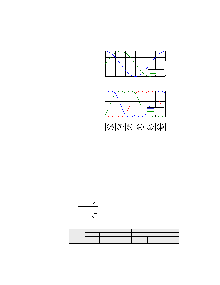
The following figures show the input Stator Reference Voltage Vector
components
u
·
and
u
‚
, corresponding sectors and output PWM signal duty
cycle ratios:
Figure 2. Standard Space Vector Modulation Technique
The following equations describe how the Space Vector Modulation PWM
signal high-times ht
A
, ht
B
, ht
C
and transition times t
low-high
and t
high-low
of each
channel are calculated:
0
60
120
180
240
300
360
0
0.1
0.2
0.3
0.4
0.5
0.6
0.7
0.8
0.9
1
Phase A
Phase B
Phase C
0
60
120
180
240
300
360
-1
-0.5
0
0.5
1
Components of the Stator Reference Voltage Vector
Standard Space Vector Modulation Technique
alpha
beta
angle
angle
dut
y
c
ycl
e
r
a
t
i
os
a
m
pl
i
t
ude
Sector 1 Sector 2 Sector 3 Sector 4 Sector 5 Sector 6
0
60
120
180
240
300
360
0
0.1
0.2
0.3
0.4
0.5
0.6
0.7
0.8
0.9
1
Phase A
Phase B
Phase C
0
60
120
180
240
300
360
-1
-0.5
0
0.5
1
Components of the Stator Reference Voltage Vector
Standard Space Vector Modulation Technique
alpha
beta
angle
angle
dut
y
c
ycl
e
r
a
t
i
os
a
m
pl
i
t
ude
0
60
120
180
240
300
360
0
60
120
180
240
300
360
0
0.1
0.2
0.3
0.4
0.5
0.6
0.7
0.8
0.9
1
Phase A
Phase B
Phase C
Phase A
Phase B
Phase C
0
60
120
180
240
300
360
0
60
120
180
240
300
360
-1
-0.5
0
0.5
1
-1
-0.5
0
0.5
1
Components of the Stator Reference Voltage Vector
Standard Space Vector Modulation Technique
alpha
beta
angle
angle
dut
y
c
ycl
e
r
a
t
i
os
a
m
pl
i
t
ude
Sector 1 Sector 2 Sector 3 Sector 4 Sector 5 Sector 6
Sector 1 Sector 2 Sector 3 Sector 4 Sector 5 Sector 6
u
T
U
=
u
T
U
=
U
=
X
2
3
Y
U
U
+
=
2
3
Z
U
U
-
=
a√1√
a√32√
a√1√
a√32√
Y√12√
Y√3√
Y√12√
Y√3√
Sector:
V.
IV.
III.
VI.
I.
II.
`√1√
`√32√
F
r
e
e
s
c
a
l
e
S
e
m
i
c
o
n
d
u
c
t
o
r
,
I
Freescale Semiconductor, Inc.
For More Information On This Product,
Go to: www.freescale.com
n
c
.
.
.