MC100ES6221
Rev 5, 04/2005
Freescale Semiconductor
Technical Data
© Freescale Semiconductor, Inc., 2005. All rights reserved.
Low Voltage 1:20 Differential
ECL/PECL/HSTL Clock Fanout Buffer
The MC100ES6221 is a bipolar monolithic differential clock fanout buffer.
Designed for most demanding clock distribution systems, the MC100ES6221
supports various applications that require the distribution of precisely aligned
differential clock signals. Using SiGe technology and a fully differential
architecture, the device offers very low skew outputs and superior digital signal
characteristics. Target applications for this clock driver is high performance clock
distribution in computing, networking and telecommunication systems.
Features
∑
1:20 differential clock fanout buffer
∑
100 ps maximum device skew
∑
SiGe technology
∑
Supports DC to 2 GHz operation of clock or data signals
∑
ECL/PECL compatible differential clock outputs
∑
ECL/PECL/HSTL compatible differential clock inputs
∑
Single 3.3 V, ≠3.3 V, 2.5 V or ≠2.5 V supply
∑
Standard 52 lead LQFP package with exposed pad for enhanced thermal
characteristics
∑
Supports industrial temperature range
∑
Pin and function compatible to the MC100EP221
∑
52-lead Pb-free Package Available
Functional Description
The MC100ES6221 is designed for low skew clock distribution systems and
supports clock frequencies up to 2 GHz. The device accepts two clock sources.
The CLK0 input can be driven by ECL or PECL compatible signals, the CLK1 input accepts HSTL compatible signals. The
selected input signal is distributed to 20 identical, differential ECL/PECL outputs. If V
BB
is connected to the CLK0 or CLK1 input
and bypassed to GND by a 10 nF capacitor, the MC100ES6221 can be driven by single-ended ECL/PECL signals utilizing the
V
BB
bias voltage output.
In order to meet the tight skew specification of the device, both outputs of a differential output pair should be terminated, even
if only one output is used. In the case where not all ten outputs are used, the output pairs on the same package side as the parts
being used on that side should be terminated.
The MC100ES6221 can be operated from a single 3.3 V or 2.5 V supply. As most other ECL compatible devices, the
MC100ES6221 supports positive (PECL) and negative (ECL) supplies. The MC100ES6221 is pin and function compatible to the
MC100EP221.
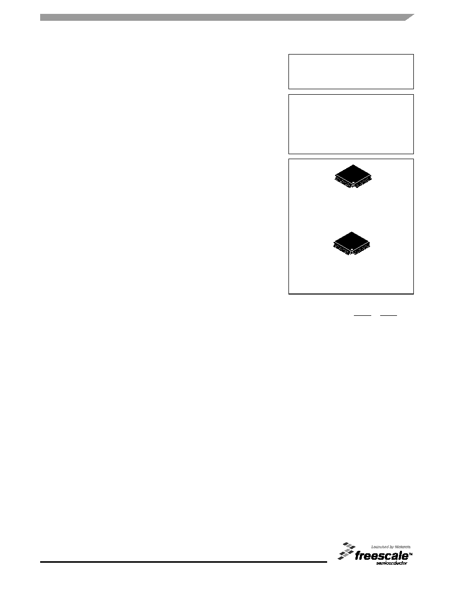
MC100ES6221
LOW VOLTAGE DUAL
1:20 DIFFERENTIAL ECL/PECL/HSTL
CLOCK FANOUT BUFFER
AE SUFFIX
52-LEAD LQFP PACKAGE
Pb-FREE PACKAGE
CASE 1336A-01
TB SUFFIX
52-LEAD LQFP PACKAGE
EXPOSED PAD
CASE 1336A-01

Advanced Clock Drivers Devices
2
Freescale Semiconductor
MC100ES6221
Figure 1. MC100ES6221 Logic Diagram
Figure 2. 52-Lead Package Pinout (Top View)
0
1
CLK0
CLK0
CLK1
CLK1
CLK_SEL
V
CC
Q0
Q0
Q1
Q1
Q2
Q2
Q3
Q3
Q16
Q16
Q17
Q17
Q18
Q18
Q19
Q19
V
BB
V
EE
V
EE
∑
∑
∑
V
EE
V
CC
∑
∑
∑
V
CC
Q5
Q5
Q4
Q4
Q3
Q3
Q2
Q2
Q1
Q1
Q0
Q0
Q12
Q12
Q13
Q13
Q14
Q14
Q15
Q15
Q16
Q16
Q17
Q17
V
CC
Q6
Q7
Q8
Q9
V
CC
V
CC
C
L
K_
SE
L
CL
K0
CL
K0
V
BB
CL
K1
CL
K1
V
EE
Q1
9
Q1
9
Q1
8
Q1
8
40
41
42
43
44
45
46
47
48
49
50
51
52
25
24
23
22
21
20
19
18
17
16
15
14
1
2
3
4
5
6
7
8
9
10 11 12 13
39 38 37 36
35 34 33 32 31 30 29 28 27
26
MC100ES6221
Q6
Q7
Q8
Q9
Q1
0
Q1
0
Q1
1
Q1
1
V
CC
Table 1. Pin Configuration
Pin
I/O
Type
Function
CLK0, CLK0
Input
ECL/PECL
Differential reference clock signal input
CLK1, CLK1
Input
HSTL
Alternative differential reference clock signal input
CLK_SEL
Input
ECL/PECL
Reference clock input select
QA[0≠19], QA[0≠19]
Output
ECL/PECL
Differential clock outputs
V
EE
(1)
1. In ECL mode (negative power supply mode), V
EE
is either ≠3.3 V or ≠2.5 V and V
CC
is connected to GND (0 V). In PECL mode (positive
power supply mode), V
EE
is connected to GND (0 V) and V
CC
is either
+3.3 V or +2.5 V. In both modes, the input and output levels are
referenced to the most positive supply (V
CC
).
Supply
Negative power supply
V
CC
Supply
Positive power supply. All V
CC
pins must be connected to the positive
power supply for correct DC and AC operation.
V
BB
Output
DC
Reference voltage output for single ended ECL and PECL operation
Table 2. Function Table
Pin
0
1
CLK_SEL
CLK0, CLK0 input pair is the reference clock. CLK0 can be
driven by ECL or PECL compatible signals.
CLK1, CLK1 input pair is the reference clock. CLK1 can be
driven by HSTL compatible signals.

Advanced Clock Drivers Devices
Freescale Semiconductor
3
MC100ES6221
Table 3. Absolute Maximum Ratings
(1)
1. Absolute maximum continuous ratings are those maximum values beyond which damage to the device may occur. Exposure to these
conditions or conditions beyond those indicated may adversely affect device reliability. Functional operation at absolute-maximum-rated
conditions is not implied.
Symbol
Characteristics
Min
Max
Unit
Condition
V
CC
Supply Voltage
≠0.3
3.6
V
V
IN
DC Input Voltage
≠0.3
V
CC
+ 0.3
V
V
OUT
DC Output Voltage
≠0.3
V
CC
+ 0.3
V
I
IN
DC Input Current
±20
mA
I
OUT
DC Output Current
±50
mA
T
S
Storage Temperature
≠65
125
∞C
T
FUNC
Functional Temperature Range
T
A
= ≠40
T
J
=
+110
∞C
Table 4. General Specifications
Symbol
Characteristics
Min
Typ
Max
Unit
Condition
V
TT
Output Termination Voltage
V
CC
≠ 2
(1)
1. Output termination voltage V
TT
= 0 V for V
CC
= 2.5 V operation is supported but the power consumption of the device will increase.
V
MM
ESD Protection (Machine Model)
200
V
HBM
ESD Protection (Human Body Model)
4000
V
CDM
ESD Protection (Charged Device Model)
2000
V
LU
Latch-Up Immunity
200
mA
C
IN
Input Capacitance
4.0
pF
Inputs
JA
,
JB
,
JC
Thermal Resistance (junction-to-ambient,
junction-to-board, junction-to-case)
See
Table 9. Thermal Resistance
∞C/W
T
J
Operating Junction Temperature
(2)
(continuous operation)
MTBF = 9.1 years
2. Operating junction temperature impacts device life time. Maximum continuous operating junction temperature should be selected according
to the application life time requirements (See application note AN1545 for more information). The device AC and DC parameters are
specified up to 110
∞C junction temperature allowing the MC100ES6221 to be used in applications requiring industrial temperature range. It
is recommended that users of the MC100ES6221 employ thermal modeling analysis to assist in applying the junction temperature
specifications to their particular application.
0
110
∞C

Advanced Clock Drivers Devices
4
Freescale Semiconductor
MC100ES6221
Table 5. PECL DC Characteristics (V
CC
= 2.5 V
± 5% or V
CC
= 3.3 V
± 5%, V
EE
= GND, T
J
= 0
∞C to + 110∞C)
Symbol
Characteristics
Min
Typ
Max
Unit
Condition
Clock Input Pair CLK0, CLK0
(1)
(PECL differential signals)
1. The input pairs CLK0, CLK1 are compatible to differential signaling standards. CLK0 is compatible to LVPECL signals and CLK1 meets both
HSTL differential signal specifications. The difference between CLK0 and CLK1 is the differential input threshold voltage (V
CMR
).
V
PP
Differential Input Voltage
(2)
2. V
PP
(DC) is the minimum differential input voltage swing required to maintain device functionality.
0.1
1.3
V
Differential operation
V
CMR
Differential Cross Point Voltage
(3)
3. V
CMR
(DC) is the crosspoint of the differential input signal. Functional operation is obtained when the crosspoint is within the V
CMR
(DC)
range and the input swing lies within the V
PP
(DC) specification.
1.0
V
CC
≠ 0.3
V
Differential operation
I
IN
Input Current
(1)
±100
µA
V
IN
= V
IL
or V
IN
= V
IH
Clock Input Pair CLK1, CLK1
(4)
(HSTL differential signals)
4. Clock inputs driven by differential HSTL compatible signals. Only applicable to CLK1, CLK1.
V
DIF
Differential Input Voltage
(5)
5. V
DIF
(DC) is the minimum differential HSTL input voltage swing required for device functionality.
0.2
1.4
V
V
X
Differential Cross Point Voltage
(6)
6. V
X
(DC) is the crosspoint of the differential HSTL input signal. Functional operation is obtained when the crosspoint is within the V
X
(DC)
range and the input swing lies within the V
PP
(DC) specification.
0
0.68 - 0.9
V
CC
≠ 0.7
V
V
IH
Input High Voltage
V
X
+ 0.1
V
X
+ 0.7
V
V
IL
Input Low Voltage
V
X
≠ 0.7
V
X
≠ 0.1
V
I
IN
Input Current
±100
µA
V
IN
= V
X
± 0.2 V
Clock Inputs (PECL single ended signals)
V
IH
Input Voltage High
V
CC
≠ 1.165
V
CC
≠ 0.880
V
V
IL
Input Voltage Low
V
CC
≠ 1.810
V
CC
≠ 1.475
V
I
IN
Input Current
(7)
7. Inputs have internal pullup/pulldown resistors which affect the input current.
±100
µA
V
IN
= V
IL
or V
IN
= V
IH
PECL Clock Outputs (Q0≠19, Q0≠19)
V
OH
Output High Voltage
V
CC
≠ 1.1
V
CC
≠ 1.005
V
CC
≠ 0.7
V
I
OH
= ≠30 mA
(8)
8. Equivalent to a termination of 50
to V
TT.
V
OL
Output Low Voltage
V
CC
≠ 1.9
V
CC
≠ 1.705
V
CC
≠ 1.4
V
I
OL
= ≠5 mA
(8)
Supply current and V
BB
I
EE
(9)
9. I
CC
calculation:
I
CC
= (number of differential output used) x (I
OH
+ I
OL
)
+ I
EE
I
CC
= (number of differential output used) x (V
OH
≠ V
TT
)
˜ R
load
+ (V
OL
≠ V
TT
)
˜ R
load
+ I
EE
.
Maximum Quiescent Supply Current without
Output Termination Current
84
160
mA
V
EE
pins
V
BB
Output Reference Voltage (f
ref
< 1.0 GHz)
(10)
10. Using V
BB
to bias unused single-ended inputs is recommended only up to a clock reference frequency of 1 GHz. Above 1 GHz, only
differential input signals should be used with the MC100ES6221.
V
CC
≠ 1.42
V
CC
≠ 1.20
V
I
BB
= 0.4 mA

Advanced Clock Drivers Devices
Freescale Semiconductor
5
MC100ES6221
Table 6. ECL DC Characteristics (V
EE
=
≠
2.5 V
± 5% or V
EE
=
≠
3.3 V
± 5%, V
CC
= GND, T
J
= 0
∞C to + 110∞C)
Symbol
Characteristics
Min
Typ
Max
Unit
Condition
Clock Input Pair CLK0, CLK0 (ECL differential signals)
V
PP
Differential Input Voltage
(1)
1. V
PP
(DC) is the minimum differential input voltage swing required to maintain device functionality.
0.1
1.3
V
Differential operation
V
CMR
Differential Cross Point Junction to top of
Package Voltage
(2)
2. V
CMR
(DC) is the crosspoint of the differential input signal. Functional operation is obtained when the crosspoint is within the V
CMR
(DC)
range and the input swing lies within the V
PP
(DC) specification.
V
EE
+ 1.0
≠0.3
V
Differential operation
I
IN
Input Current
(1)
±100
µA
V
IN
= V
IL
or V
IN
= V
IH
Clock Inputs (ECL single ended signals)
V
IH
Input Voltage High
≠1.165
≠0.880
V
V
IL
Input Voltage Low
≠1.810
≠1.475
V
I
IN
Input Current
(3)
3. Inputs have internal pullup/pulldown resistors which affect the input current.
±100
µA
V
IN
= V
IL
or V
IN
= V
IH
ECL Clock Outputs (Q0≠A19, Q0≠Q19)
V
OH
Output High Voltage
≠1.1
≠1.005
≠0.7
V
I
OH
= ≠30 mA
(4)
4. Equivalent to a termination of 50
to V
TT
.
V
OL
Output Low Voltage
≠1.9
≠1.705
≠1.4
V
I
OL
= ≠5 mA
(4)
Supply Current and V
BB
I
EE
(5)
5. I
CC
calculation:
I
CC
= (number of differential output used) x (I
OH
+ I
OL
) + I
EE
I
CC
= (number of differential output used) x (V
OH
≠ V
TT
)
˜ R
load
+ (V
OL
≠ V
TT
)
˜ R
load
+ I
EE
.
Maximum Quiescent Supply Current without
Output Termination Current
84
160
mA
V
EE
pins
V
BB
Output Reference Voltage (f
ref
< 1.0 GHz)
(6)
6. V
BB
can be used to bias unused single-ended inputs up to a clock reference frequency of 1 GHz. Above 1 GHz, only differential signals
should be used with the MC100ES6221.
≠1.42
≠1.20
V
I
BB
= 0.4 mA
Advanced Clock Drivers Devices
6
Freescale Semiconductor
MC100ES6221
Table 7. AC Characteristics (ECL: V
EE
=
≠
3.3 V
±
5% or V
EE
=
≠
2.5 V
±
5%, V
CC
= GND) or
(PECL: V
CC
= 3.3 V
±
5% or V
CC
= 2.5 V
±
5%, V
EE
= GND, T
J
= 0
∞C to + 110∞C)
(1)
1. AC characteristics apply for parallel output termination of 50
to V
TT
.
Symbol
Characteristics
Min
Typ
Max
Unit
Condition
Clock Input Pair CLK0, CLK0 (PECL or ECL differential signals)
V
PP
Differential Input Voltage
(2)
(peak-to-peak)
2. V
PP
(AC) is the minimum differential ECL/PECL input voltage swing required to maintain AC characteristics including t
PD
and
device-to-device skew.
0.2
1.3
V
V
CMR
Differential Input Crosspoint Voltage
(3)
PECL
ECL
3. V
CMR
(AC) is the crosspoint of the differential ECL/PECL input signal. Normal AC operation is obtained when the crosspoint is within the
V
CMR
(AC) range and the input swing lies within the V
PP
(AC) specification. Violation of V
CMR
(AC) or V
PP
(AC) impacts the device
propagation delay, device and part-to-part skew.
1.0
V
EE
+ 1.0
V
CC
≠ 0.3
≠0.3 V
V
V
f
CLK
Input Frequency
0
2000
MHz
Differential
t
PD
Propagation Delay CLK0 to Q0-19
400
540
670
ps
Differential
Clock Input Pair CLK1, CLK1 (HSTL differential signals)
V
DIF
Differential Input Voltage
(4)
(peak-to-peak)
4. V
DIF
(AC) is the minimum differential HSTL input voltage swing required to maintain AC characteristics including t
PD
and device-to-device
skew. Only applicable to CLKB.
0.2
1.3
V
V
X
Differential Input Crosspoint Voltage
(5)
5. V
X
(AC) is the crosspoint of the differential HSTL input signal. Normal AC operation is obtained when the crosspoint is within the V
X
(AC)
range and the input swing lies within the V
DIF
(AC) specification. Violation of V
X
(AC) or V
DIF
(AC) impacts the device propagation delay,
device and part-to-part skew.
0.1
0.68≠0.9
V
CC
≠ 1.0
V
f
CLK
Input Frequency
0
1000
MHz
Differential
t
PD
Propagation Delay CLK1 to Q0≠19
650
780
950
ps
Differential
PECL/ECL Clock Outputs (Q0≠19, Q0≠19)
V
O(P-P)
Differential Output Voltage (peak-to-peak)
f
O
< 1.0 GHz
f
O
< 2.0 GHz
0.375
TDB
0.630
0.250
V
V
t
sk(O)
Output-to-Output Skew
50
100
ps
Differential
t
sk(PP)
Output-to-Output Skew (part-to-part)
using CLK0
using CLK1
parts at one given T
J
, V
CC
, f
ref
270
300
250
ps
ps
ps
Differential
t
JIT(CC)
Output Cycle-to-Cycle Jitter
RMS (1
)
1
ps
t
SK(P)
DC
Q
Output Pulse Skew
(6)
Output Duty Cycle
f
REF
< 0.1 GHz
f
REF
< 1.0 GHz
6. Output pulse skew is the absolute difference of the propagation delay times: | t
pLH
≠ t
pHL
|.
49.5
45.0
30
50
50
50
50.5
55.0
ps
%
%
DC
REF
= 50%
DC
REF
= 50%
t
r
, t
f
Output Rise/Fall Time
50
350
ps
20% to 80%

Advanced Clock Drivers Devices
Freescale Semiconductor
7
MC100ES6221
Figure 3. MC100ES6221 Test Reference
Figure 4. MC100ES6221 AC Test Reference Measurement Waveform
Differential Pulse
Generator
Z = 50
R
T
= 50
Z
0
= 50
DUT
MC100ES6221
V
TT
R
T
= 50
Z
0
= 50
V
TT
t
PD
(CLK
N
to Q
X
)
V
CMR
= V
CC
≠ 1.3 V
V
PP
= 0.8 V
CLK
N
CLK
N
Q
X
Q
X

Advanced Clock Drivers Devices
8
Freescale Semiconductor
MC100ES6221
APPLICATIONS INFORMATION
Understanding the Junction Temperature Range of the
MC100ES6221
To make the optimum use of high clock frequency and low
skew capabilities of the MC100ES6221, the MC100ES6221
is specified, characterized and tested for the junction
temperature range of T
J
= 0
∞C to +110∞C. Because the exact
thermal performance depends on the PCB type, design,
thermal management and natural or forced air convection,
the junction temperature provides an exact way to correlate
the application specific conditions to the published
performance data of this data sheet. The correlation of the
junction temperature range to the application ambient
temperature range and vice versa can be done by
calculation:
T
J
= T
A
+ R
thja
P
tot
Assuming a thermal resistance (junction to ambient) of
17
∞C/W (2s2p board, 200 ft/min airflow, see
Table 8
) and a
typical power consumption of 1148 mW (all outputs
terminated 50 ohms to V
TT
, V
CC
= 3.3 V, frequency
independent), the junction temperature of the MC100ES6221
is approximately T
A
+ 21∞C, and the minimum ambient
temperature in this example case calculates to
≠
21
∞C (the
maximum ambient temperature is 89
∞C. See
Table 8
).
Exceeding the minimum junction temperature specification of
the MC100ES6221 does not have a significant impact on the
device functionality. However, the continuous use the
MC100ES6221 at high ambient temperatures requires
thermal management to not exceed the specified maximum
junction temperature. Please see the application note
AN1545 for a power consumption calculation guideline.
Maintaining Lowest Device Skew
The MC100ES6221 guarantees low output-to-output bank
skew of 50 ps and a part-to-part skew of max. 270 ps. To
ensure low skew clock signals in the application, both outputs
of any differential output pair need to be terminated
identically, even if only one output is used. When fewer than
all nine output pairs are used, identical termination of all
output pairs within the output bank is recommended. This will
reduce the device power consumption while maintaining
minimum output skew.
Power Supply Bypassing
The MC100ES6221 is a mixed analog/digital product. The
differential architecture of the MC100ES6221 supports low
noise signal operation at high frequencies. In order to
maintain its superior signal quality, all V
CC
pins should be
bypassed by high-frequency ceramic capacitors connected
to GND. If the spectral frequencies of the internally generated
switching noise on the supply pins cross the series resonant
point of an individual bypass capacitor, its overall impedance
begins to look inductive and thus increases with increasing
frequency. The parallel capacitor combination shown ensures
that a low impedance path to ground exists for frequencies
well above the noise bandwidth.
Figure 5. V
CC
Power Supply Bypass
Table 8. Ambient Temperature Ranges (P
tot
= 1148 mW)
R
thja
(2s2p board)
T
A, min
(1)
1. The MC100ES6221 device function is guaranteed from
T
A
= ≠40
∞C to T
J
= 110
∞C
T
A, max
Natural convection
20
∞C/W
≠23
∞C
87
∞C
100 ft/min
18
∞C/W
≠21
∞C
89
∞C
200 ft/min
17
∞C/W
≠20
∞C
90
∞C
400 ft/min
16
∞C/W
≠18
∞C
92
∞C
800 ft/min
15
∞C/W
≠17
∞C
93
∞C
V
CC
MC100ES6221
V
CC
33...100 nF
0.1 nF

Advanced Clock Drivers Devices
Freescale Semiconductor
9
MC100ES6221
APPLICATIONS INFORMATION
Using the Thermally Enhanced Package of the
MC100ES6221
The MC100ES6221 uses a thermally enhanced exposed
pad (EP) 52 lead LQFP package. The package is molded so
that the lead frame is exposed at the surface of the package
bottom side. The exposed metal pad will provide the low
thermal impedance that supports the power consumption of
the MC100ES6221 high-speed bipolar integrated circuit and
eases the power management task for the system design. A
thermal land pattern on the printed circuit board and thermal
vias are recommended in order to take advantage of the
enhanced thermal capabilities of the MC100ES6221. Direct
soldering of the exposed pad to the thermal land will provide
an efficient thermal path. In multilayer board designs, thermal
vias thermally connect the exposed pad to internal copper
planes. Number of vias, spacing, via diameters and land
pattern design depend on the application and the amount of
heat to be removed from the package. A nine thermal via
array, arranged in a 3 x 3 array and using a 1.2 mm pitch in
the center of the thermal land is a requirement for
MC100ES6221 applications on multi-layer boards. The
recommended thermal land design comprises a 3 x 3 thermal
via array as shown in
Figure 6
, providing an efficient heat
removal path.
Figure 6. Recommended Thermal Land Pattern
The via diameter is should be approx. 0.3 mm with 1 oz.
copper via barrel plating. Solder wicking inside the via
resulting in voids during the solder process must be avoided.
If the copper plating does not plug the vias, stencil print solder
paste onto the printed circuit pad. This will supply enough
solder paste to fill those vias and not starve the solder joints.
The attachment process for exposed pad package is
equivalent to standard surface mount packages.
Figure 7
shows a recommend solder mask opening with respect to the
recommended 3 x 3 thermal via array. Because a large solder
mask opening may result in a poor release, the opening
should be subdivided as shown in
Figure 7
. For the nominal
package standoff 0.1 mm, a stencil thickness of 5 to 8 mils
should be considered.
Figure 7. Recommended Solder Mask Openings
For thermal system analysis and junction temperature
calculation the thermal resistance parameters of the package
is provided:
It is recommended that users employ thermal modeling
analysis to assist in applying the general recommendations
to their particular application. The exposed pad of the
MC100ES6221 package does not have an electrical low
impedance path to the substrate of the integrated circuit and
its terminals. The thermal land should be connected to GND
through connection of internal board layers.
4.8
Thermal via array (3x3),
1.2 mm pitch,
0.3 mm diameter
Exposed pad
land pattern
all units mm
4.
8
Table 9. Thermal Resistance
(1)
1. Applicable for a 3 x 3 thermal via array.
ConvectionL
FPM
R
THJA
(2)
∞C/W
2. Junction to ambient, four conductor layer test board (2S2P), per
JES51≠7 and JESD 51≠5.
R
THJA
(3)
∞C/W
3. Junction to ambient, single layer test board, per JESD51≠3.
R
THJC
∞C/W
R
THJB
(4)
∞C/W
4. Junction to board, four conductor layer test board (2S2P) per
JESD 51≠8.
Natural
20
48
4
(5)
29
(6)
5. Junction to exposed pad.
6. Junction to top of package.
16
100
18
47
200
17
46
400
16
43
800
15
41
Exposed pad land
pattern
4.8
Thermal via array (3x3),
1.2 mm pitch,
0.3 mm diameter
1.0
0.2
all units mm
4.
8
1.0
0.2

Advanced Clock Drivers Devices
10
Freescale Semiconductor
MC100ES6221
PACKAGE DIMENSIONS
NOTES:
1.
2.
3.
4.
5.
6.
7.
8.
DIMENSIONS ARE IN MILLIMETERS.
INTERPRET DIMENSIONS AND TOLERANCES PER
ASME Y14.5M, 1994.
DATUMS A, B AND D TO BE DETERMINED AT DATUM
PLANE H.
DIMENSION TO BE DETERMINED AT SEATING PLANE
C.
THIS DIMENSION DOES NOT INCLUDE DAMBAR
PROTRUSION. ALLOWABLE DAMBAR PROTRUSION
SHALL NOT CAUSE THE LEAD WIDTH TO EXCEED
0.46 mm. DAMBAR CANNOT BE LOCATED ON THE
LOWER RADIUS OR THE FOOT. MINIMUM SPACE
BETWEEN PROTRUSION AND ADJACENT LEAD
SHALL NOT BE LESS THAN 0.07 mm.
THIS DIMENSION DOES NOT INCLUDE MOLD
PROTRUSION. ALLOWABLE PROTRUSION IS 0.25mm
PER SIDE. THIS DIMENSION IS MAXIMUM PLSTIC
BODY SIZE DIMENSION INCLUDING MOLD MISMATCH.
EXACT SHAPE OF EACH CORNER IS OPTIONAL.
THESE DIMENSIONS APPLY TO THE FLAT SECTION
OF THE LEAD BETWEEN 0.10mm AND 0.25mm FROM
THE LEAD TIP.
52
0.2 H A-B D
1
40
39
14
13
26
27
B
5
10
4X
4X 13 TIPS
0.2 C A-B D
A
D
PIN 1
INDEX
7
6
5
6
12
10
12
4
4
4
4
6
6
6
6
B
B
0.65
48X
X=A, B OR D
CL
VIEW Y
X
0.05
0.25
GAUGE PLANE
1.3
(0.2)
R
(1)
0.75
0.20
VIEW AA
7∞
1.5
0.05
0.45
0∞ MIN 0.20
0.08
0∞
R
0.20
0.08
(12∞)
4X
SEATING
PLANE
1.7 MAX
VIEW AA
0.1 C
C
H
A-B
M
0.08
D
C
52X
0.40
J
J
0.22
52X
5
(12∞)
4X
SECTION B-B
0.20
PLATING
BASE METAL
8
8
8
8
0.35
(0.3)
0.09
0.20
0.07
0.16
4.78
4.58
VIEW J-J
EXPOSED PAD
VIEW Y
4.78
4.58
CASE 1336A-01
ISSUE O
52-LEAD LQFP PACKAGE

Advanced Clock Drivers Devices
Freescale Semiconductor
11
MC100ES6221
NOTES

How to Reach Us:
Home Page:
www.freescale.com
E-mail:
support@freescale.com
USA/Europe or Locations Not Listed:
Freescale Semiconductor
Technical Information Center, CH370
1300 N. Alma School Road
Chandler, Arizona 85224
+1-800-521-6274 or +1-480-768-2130
support@freescale.com
Europe, Middle East, and Africa:
Freescale Halbleiter Deutschland GmbH
Technical Information Center
Schatzbogen 7
81829 Muenchen, Germany
+44 1296 380 456 (English)
+46 8 52200080 (English)
+49 89 92103 559 (German)
+33 1 69 35 48 48 (French)
support@freescale.com
Japan:
Freescale Semiconductor Japan Ltd.
Headquarters
ARCO Tower 15F
1-8-1, Shimo-Meguro, Meguro-ku,
Tokyo 153-0064
Japan
0120 191014 or +81 3 5437 9125
support.japan@freescale.com
Asia/Pacific:
Freescale Semiconductor Hong Kong Ltd.
Technical Information Center
2 Dai King Street
Tai Po Industrial Estate
Tai Po, N.T., Hong Kong
+800 2666 8080
support.asia@freescale.com
For Literature Requests Only:
Freescale Semiconductor Literature Distribution Center
P.O. Box 5405
Denver, Colorado 80217
1-800-441-2447 or 303-675-2140
Fax: 303-675-2150
LDCForFreescaleSemiconductor@hibbertgroup.com
MC100ES6221
Rev. 5
04/2005
Information in this document is provided solely to enable system and software
implementers to use Freescale Semiconductor products. There are no express or
implied copyright licenses granted hereunder to design or fabricate any integrated
circuits or integrated circuits based on the information in this document.
Freescale Semiconductor reserves the right to make changes without further notice to
any products herein. Freescale Semiconductor makes no warranty, representation or
guarantee regarding the suitability of its products for any particular purpose, nor does
Freescale Semiconductor assume any liability arising out of the application or use of any
product or circuit, and specifically disclaims any and all liability, including without
limitation consequential or incidental damages. "Typical" parameters that may be
provided in Freescale Semiconductor data sheets and/or specifications can and do vary
in different applications and actual performance may vary over time. All operating
parameters, including "Typicals", must be validated for each customer application by
customer's technical experts. Freescale Semiconductor does not convey any license
under its patent rights nor the rights of others. Freescale Semiconductor products are
not designed, intended, or authorized for use as components in systems intended for
surgical implant into the body, or other applications intended to support or sustain life,
or for any other application in which the failure of the Freescale Semiconductor product
could create a situation where personal injury or death may occur. Should Buyer
purchase or use Freescale Semiconductor products for any such unintended or
unauthorized application, Buyer shall indemnify and hold Freescale Semiconductor and
its officers, employees, subsidiaries, affiliates, and distributors harmless against all
claims, costs, damages, and expenses, and reasonable attorney fees arising out of,
directly or indirectly, any claim of personal injury or death associated with such
unintended or unauthorized use, even if such claim alleges that Freescale
Semiconductor was negligent regarding the design or manufacture of the part.
FreescaleTM and the Freescale logo are trademarks of Freescale Semiconductor, Inc.
All other product or service names are the property of their respective owners.
© Freescale Semiconductor, Inc. 2005. All rights reserved.